Home » Posts tagged 'tablet PC'
Tag Archives: tablet PC
H2CY13: Upcoming next-gen Nexus 7, the ASUS MeMO Pad HD 7 “re-incarnation” at reduced by $50 price, dual/quad-core mid-range tablets from white-box vendors starting from $65
(while entry level will start from $40) … with that there would be tremendous pressure on low-volume tablet supliers (branded or white-box alike), as well as Samsung and Apple. Meanwhile China strengthens its position as the world leading PC Market.
Complementary post reminder:
Eight-core MT6592 for superphones and big.LITTLE MT8135 for tablets implemented in 28nm HKMG are coming from MediaTek to further disrupt the operations of Qualcomm and Samsung [‘Experiencing the Cloud’, July 20, 2013] from which the following excerpts I will include here as the ones directly related to the content given here as well:

At the end of July the launch of a tablet chip is expected: the MT8135, with 2xA15 +2xA7, still using an Imagination GPU, and mainly targeting the high-end tablet market. If Google OS will be closed and converged that will have a huge impact on us.
… We will use Windows as a second priority, while using Firefox [OS] and HTML5 as a secondary backup, by keeping track of them. Because we judge that the [Android] OS convergence from Google profitability point of view is very low, therefore our vote for these two emerging open OS’s is in the ‘not so urgent’ category, in addition to and outside of Android. The other focus is again on Windows Phone 8. For the moment, however, WP8 hardware configuration requirements are still higher (mainly memory), power consumption – after optimizing the gap with Android – is not too large.
End of the complementary post reminder
Rumor: New Nexus 7 specs, features and launch details mentioned in chat with Asus rep [Android Authority, June 30, 2013]
AE: The Tablet should be released before the ending of Q2
C: when exactly is before Q2?
AE: That will be before the ending of July…
AE: There has not been confirmed specification as yet, but here is some basics specification , that you can look at:
7 inch LED with 1980*1200 resolution
Qualcomm Snapdragon 600 Quad Core CPU / Snapdragon APQ8064 CPU
2GB of RAM
32GB internal storage
5Mpx rear camera and 1.2Mpx front camera
Android 4.3
4000mAh battery
Wifi a/b/g/n,Bluetooth 4.0 and NFC enabled
LTE / WCDMA / GSM supportThis is not confirmed specifications but you can review it
vs. the first one: Nexus 7: Google wanted it in 4 months for $199/$245, ASUS delivered + Nexus Q (of Google’s own design and manufacturing) added for social streaming from Google Play to speakers and screen in home under Android device control [‘Experiencing the Cloud’, June 28, 2012] which already has an ASUS only “reincarnation:
Experience MeMO Pad HD 7 [asus YouTube channel, June 16, 2013]
- 7-inch HD [1280 x 800] tablet with a wide-view angle IPS display for stunning visuals
- Rear 5MP and front 1.2MP dual cameras to capture the moments
- Dual stereo speakers with Sonicmaster Technology for incredible sound effect.
- Ultra light, weighs only 302g
- Up to 10 hrs battery life to make it through your day
ASUS Announces MeMO Pad HD 7 and MeMO Pad FHD 10 Tablets [press release, June 3, 2013]
ASUS MeMO Pad™ HD 7 — the value tablet for mobile entertainment
ASUS MeMO Pad™ HD 7 has a quad-core processor and 1GB RAM for smooth and responsive performance with apps of all kinds. The 7-inch display has a 1280 x 800 native resolution for crisp text and images, and IPS technology for accurate, vibrant colors with 170-degree wide viewing angles. MeMO Pad™ HD 7 also features high-quality stereo speakers with enhanced sound, courtesy of ASUS SonicMaster audio technology.MeMO Pad™ HD 7 has a 1.2-megapixel front-facing HD camera that can capture 720p HD videos and models are also available with a rear 5-megapixel camera. Just 10.8mm thick and 302g, the feature-packed MeMO Pad™ HD 7 has a lithium polymer battery that lasts for up to 10 hours with 720p video playback. Models are available in four colors — black, white, pink and green.
MeMO Pad™ HD 7 has 16GB of storage and a MicroSD card slot, plus 16GB ASUS WebStorage free for one year. Together with the ASUS WebStorage Office, users can view, create, edit and share Microsoft Office documents online.
AVAILABILITY & PRICING
ASUS MeMO Pad™ HD 7 has an MSRP of US$129 for 8GB capacity and US$149 for 16GB [a “follow up” to the $199 Nexus 7 tablet developed jointly by Google and ASUS and announced a year ago], and will be available starting in July 2013.
Asustek and HP enter China tablet market with entry-level models [DIGITIMES, July 1, 2013]
Asustek Computer and Hewlett-Packard (HP) are both set to enter the China tablet market with new cheap tablet models: the Asustek 7-inch 8GB MeMO Pad HD 7, priced below CNY999 (US$163) and HP Slate 7, priced at CNY999 [$163], according to sources from channel retailers.
Asustek’s 8GB MeMO Pad HD 7 will be supplied to the China market exclusively and is expected to appear later in July.
Prior to Asustek and HP, Acer already offered its 7-inch Iconia B1-A71 tablet [1.2GHz dual-core MT8317T based] at CNY699 [$114], while Lenovo is pushing its A1000 for a price of CNY999 [$163].
Compared to first-tier vendors, most China-based white-box tablet players are offering their products at prices between CNY299-500[$49-81.5], giving them advantages in pricing, but first-tier vendors still outmatch white-box players in product quality, specifications and after-sales service, the sources said.
Currently this is the best 7” quad-core offering from purely mainland China technology:
7” quad-core Allwinner A31s based Onda tablets for $65 (v701s) and $81 with IPS (v711s) in China, while for $89 and $99 outside [‘USD 99 Allwinner’, June 22, 2013] for which here is the Onda V711s Quad Core A31s 7″ IPS Tablet PC In-depth Review [dealsprime YouTube channel, June 24, 2013]
With and 1280×800 resolution Onda V712 quad-core version is available from April 8, 2013. The current price for Onda V712 Quad Core RAM 2GB 7 Inch IPS Screen Android Tablet 16GB outside China is $139 (699 yuan, $114 inside). It has 0.3MP front and 2MP back camera (vs. 1.2MP front and 5MP rear on ASUS MeMO Pad HD 7), but its video capability is 4K.
Meanwhile the cheapest dual-core mid-range tablet from white-box vendors is the new ICOO D70PR03 for 399 yuan i.e $65. This is with 1.2GHz Allwinner A20 SoC and 1024×600 IPS screen.
China white-box tablet players seeing success in landing government procurement orders [DIGITIMES, July 1, 2013]
China-based white-box players are gaining the upper hand in the competition with first-tier brand vendors for tablet procurement orders from Asia Pacific governments due to their advantages in pricing, while improved product quality and stability also helped the white-box players to narrow their gap with first-tier players, according to sources from tablet players.
The government in Thailand recently released procurement orders for 1.6 million education-purpose tablets which were mostly taken by a China-based white-box player, and first-tier vendors are having trouble competing due to considerations about profitability, the sources noted.
The sources pointed out that the white-box maker landed orders for a total of 800,000 tablets from the Thailand government worth NT$1.57 billion (US$52.35 million), equivalent to a price of NT$1,900-2,000 [US$63-67] for each device.
However, even with such a low price, the sources believe the white-box maker is still profiting from the orders.
Currently, an entry-level 7-inch tablet from a China white-box player is priced at about US$50 and can go up to US$70-90 in the retail channel, giving them strong advantages in price competition.
Although first-tier brand vendors are also aggressively trying to enter the entry-level tablet market, white-box players are still expected to achieve shipments of 120 and 170 million units in 2013 and 2014, respectively.
Thailand school kids get tablet computers [Aljazeera via AussieNews1 YouTube channel, Aug 23, 2012]
Surprise auction winners [Bangkok Post, June 29, 2013]
Dark horses Shenzhen Yitoa Intelligent Control Co of China and Supreme Distribution (Thailand) won yesterday’s bidding for the second phase of the One Tablet per Child scheme to supply 1.22 million tablets, beating out Shenzhen Scope Scientific Development.
The Chinese firm clinched the bid for the first and second zones, while the Thai company won the contract for the third zone.
The Office of the Basic Education Commission (Obec) held an e-auction for the tablets yesterday seeking bidding winners to supply 1.63 million tablets.
Education Minister Phongthep Thepkanchana said Shenzhen Yitoa won a bid to supply 431,105 tablets for Prathom 1 students worth 842 million baht for the first zone in central and southern provinces.
The company offered a price of 1,953.12 baht [$63] per tablet, 28.2% lower than the median price set at 2,720 baht each.

According to earlier information: “The tablet will have government specifications of a seven-inch display with a camera resolution of 1024×600 pixels, a minimum 1.5-gigahertz dual-core processor unit, one gigabyte of RAM, eight gigabytes of storage memory, 3,600 milliampere hours of lithium polymer battery life, and continuous Wi-Fi internet access for at least three hours.”
The Chinese firm also won the bid to supply 373,637 tablets for Prathom 1 students worth 786 million baht for the second zone in the northern and northeastern provinces.
The company offered 2,103.64 baht [$67.5] per unit, 22.7% below the median price.
Supreme Distribution, meanwhile, proposed the lowest price for tablets in the third zone, covering Mathayom 1 students in the central and southern provinces, at 2,908.24 baht [$93], down slightly from the median price of 2,920 baht.
The Thai computer assembly firm will supply 426,683 tablets worth 1.24 billion baht.
Obec postponed the bid for the fourth zone – covering some northern and northeastern provinces – to July, as Shenzhen Yitoa was the only bidder in the auction. The conditions require at least two bidders in competition.
Mr Phongthep said purchasing contracts are expected to be sealed in the week ahead. All winners are obliged to deliver their tablets within 90 days of signing contracts.
Panuwat Khantamoleekul, the managing director of Supreme Distribution, said the company could not offer a sharp rate cut since Mathayom 1 specifications are higher than those for Prathom 1.
He said his company will build its own factory in Thailand to assemble materials sourced from China.
It set up a local office here two decades ago and also won an earlier bid to supply tablets in Russia.
Shenzhen Yitoa Digital Appliance Co. Ltd [Global Sources, April 14, 2013]
Offering a Wide Range of Electronic Products
Shenzhen Yitoa Digital Appliance was founded in 2007, which is affiliated to Shenzhen Yitoa Intelligent Control Co., Ltd. We are a nationally known enterprise designing, developing, manufacturing and selling intelligent controllers of digital equipment. Our main products include e-book readers, MIDs, tablet PCs and other devices.Releasing Three New Products Monthly
Every year, we invest $800,000 in our R&D department to innovate and renew users’ digital life. This gives our 100 experienced engineers the resources they need to add up to three new products a month. Simply send us your OEM/ODM requirements, and we’ll complete a sample for you in as fast as one week. Now our company cooperates with Aigo, Newsman, Skyworth and other national famous companies.Recipient of International Certifications and Recognitions
With a 16,000-square-meter factory, 100 engineers, 1,600 workers and 25 assembly lines, our monthly capacity is over 1 million pieces. For your assurance, all of our products carry CE, CQC, CCC, UL and VED approvals, and are manufactured under ISO 9001:2000 and ISO 14001:2004 guidelines. Moreover, we have been recognized as a hi-tech enterprise in 2004, one of the top 100 Shenzhen Software Enterprises in 2005, and one of the top 20 Shenzhen Software Export Enterprises in 2006.
Leading Tablet PC Brands Reduce 2013 Targets [DisplaySearch blog, June 27, 2013]
We recently pointed out [Smaller Tablets to Get Even More Popular in the Second Half of 2013 [DisplaySearch blog, June 18, 2013]] that 2013 would be the year in which smaller tablet PC shipments (especially 7” and 8”) would surpass larger tablet PC shipments (such as 9.7” and 10.1”). Tablet PCs are starting to overlap with larger smart phones, as well as with ultra-slim notebook PCs.
Our latest forecast for the tablet PC market in the Quarterly Mobile PC Shipment and Forecast Report is for 67% Y/Y growth – from 153.6M in 2012 to 256.5M in 2013. Within this growing market, the share held by the top 12 brands, including Apple, HP, Acer, Dell, Lenovo, ASUS, Samsung, Toshiba, Sony, Amazon, Google, and Microsoft, is falling because the whitebox market [iPad-sized Tablets No Longer Driving Panel Growth Momentum [DisplaySearch blog, June 27, 2013]], especially in China, is growing faster. We estimate that the top brands, which shipped a combined 104.2M units in 2012, have reduced their 2013 shipment plans from 172M forecast in April to 167M forecast in June.
Apple’s iPad series accounted for 67M units in 2012 and remains the market leader, but is also the leading example of this trend. We estimate that Apple originally planned to ship 88M iPads in 2013, has reduced its target to 74M, including 31M iPads and 43M iPad minis.
We estimate that Samsung’s total tablet PC and phablet business plan is nearly 50M units in 2013, a big jump from 15.6M in 2012. Samsung plans include 39.5M tablet PCs, and 10M Galaxy Mega series (5.8” and 6.3”; while Samsung defines these as phablets, we classify them as smart phones).
Other tablet PC brands expect to grow their business in 2013. Among them, Lenovo, Microsoft, HP, and Acer are the most aggressive. Lenovo has two product lines for its tablet PC – X86 and ARM series. In 2013, Lenovo is planning for 3M X86 and 8M ARM.
Tablet PCs and Touch Adoption Expected to Drive Mobile PC Shipments Through 2017, According to NPD DisplaySearch [press release, May 6, 2013]
SANTA CLARA, CALIF., May 6, 2013—The mobile PC market is expected to increase from 367.6 million units shipped in 2012 to 762.7 million globally by 2017, driven by touch-enabled form factors, according to the NPD DisplaySearch Quarterly Mobile PC Shipment and Forecast Report. The majority of this shift will come as tablet PCs begin to replace notebook PCs this year as the dominant mobile PC form factor, and touch becomes a key feature in mobile PC adoption.
“The mobile PC industry is undergoing significant change this year,” said Richard Shim, senior analyst with NPD DisplaySearch. “The rapid rise and establishment of white box tablet PCs (tablets made by small local brands, mainly in China) is putting pressure on traditional notebook PCs. These low-cost tablets are reaching further into emerging regions where notebook PC penetration rates have remained low, resulting in cannibalization by tablet PCs.”
Tablet PC shipments are forecast to increase 67% Y/Y to 256.5 million in 2013, and reach 579.4 million by 2017. White box tablet PCs accounted for one-third of tablet PC shipments in 2012 and will maintain at that level for the next several years.
Notebook PC shipments are expected to decline 10% over the next four years, from 203.3 million in 2013 to 183.3 million in 2017, but there will be pockets of growth. Shipments of notebooks with touch capabilities are expected to grow 48% Y/Y in 2014. In the notebook category, touch will be used mainly in ultra-slim PCs, which includes Intel-specified Ultrabooks, the MacBook Air, and other slim form factor notebooks. Ultra-slims, which are at the premium end of the notebook market, are forecast to account for two-thirds of touch-enabled notebooks in 2013. By 2017, they will be 80%. Intel’s recent mandate that third-generation Ultrabooks (using the company’s next generation Haswell processors) must include touch will also help adoption.
Figure 1: Global Mobile PC Shipments, 2012-2017

Source: NPD DisplaySearch Quarterly Mobile PC Shipment and Forecast Report
New operating systems such as Windows 8 are unlikely to be a major driver of touch adoption. Rather, penetration of touch in notebook PCs will be driven by a reduction in cost and new form factors, such as hybrids, sliders, and convertibles.
“Thus far, Windows 8 has had a limited impact on driving touch adoption in notebook PCs, due to a lack of applications needing touch and the high cost of touch on notebook PCs,” added Shim. “Form factors aimed at differentiation from standard clamshell notebooks will help to drive consumer adoption of touch-enabled notebook PCs, starting in the second half of 2013.”
The NPD DisplaySearch Quarterly Mobile PC Shipment and Forecast Report covers the entire range of mobile PC products shipped worldwide and regionally. With analysis of global and regional brands, the Quarterly Mobile PC Shipment and Forecast Report provides an objective, expert view of the market with insight into historical shipments, revenues, forecasts, and more. For more information about the report, please contact Charles Camaroto at 1.888.436.7673 or 1.516.625.2452, e-mail contact@displaysearch.com or contact your regional NPD DisplaySearch office in China, Japan, Korea or Taiwan for more information.
About NPD DisplaySearch
NPD DisplaySearch, part of The NPD Group, provides global market research and consulting specializing in the display supply chain, including trend information, forecasts and analyses developed by a global team of experienced analysts with extensive industry knowledge. NPD DisplaySearch supply chain expertise complements sell-through information from The NPD Group, thereby providing a true end-to-end view of the display supply chain from materials and components to shipments of electronic devices with displays to sales of major consumer and commercial channels. For more information, visit us at http://www.displaysearch.com/. Read our blog at http://www.displaysearchblog.com/ and follow us on Twitter at @DisplaySearch.
About The NPD Group, Inc.
The NPD Group provides global information and advisory services to drive better business decisions. By combining unique data assets with unmatched industry expertise, we help our clients track their markets, understand consumers, and drive profitable growth. Sectors covered include automotive, beauty, consumer electronics, entertainment, fashion, food/foodservice, home, luxury, mobile, office supplies, sports, technology, toys, and video games. For more information, visithttp://www.npd.com/ and npdgroupblog.com. Follow us on Twitter: @npdtech and @npdgroup.
China [branded] smartphone vendors to foray into tablet segment [DIGITIMES, July 1, 2013]
China-based smartphone vendors, including Huawei, ZTE, Lenovo and Xiaomi Technology, all will step up their efforts to penetrate the tablet market, according to industry sources.
Huawei plans to launch a new 7-inch tablet in the third quarter of 2013, and together with a 10.1-inch model released in early 2013, Huawei is sourcing about two million flat panels from China-based Truly Opto-electronics currently, the sources indicated.
Meanwhile, Huawei also purchases a portion of displays used in its new tablets from Innolux. However, the Taiwan-based flat panel maker declined to comment on orders from individual clients.
Lenovo also unveiled its Windows 8-based tablet, the Lenovo Miix10, recently. The Lenovo Miix, which is expected to hit the market in the third quarter, is equipped with a 10.1-inch 1366 by 768 IPS display and is power by an Intel dual-core Atom processor.
Xiaomi reportedly will step into the tablet segment by unveiling its first tablet in mid-August, the sources revealed, adding that Xiaomi will utilize tablet chipset solutions from MediaTek.
White-box vendors expected to lower prices for entry-level 7-inch tablets to US$40 in 2H13 [DIGITIMES, June 7, 2013]
The market for 7-inch tablets is seeing intense competition and white-box vendors are expected to further reduce prices for entry-level models to US$40 in the second half of 2013, according to Taiwan-based supply chain sources.
Entry-level white-box tablets are expected to continue selling well in markets such as China, and supply chains are able to increasingly decrease pricing for entry-level components, said the sources.
Meanwhile, Digitimes Research predicts that 254 million tablets will be sold in 2013, up 63.9% on year.
China-based white-box 2013 tablet shipments likely below forecasts [DIGITIMES, June 14, 2013]
China-based white-box tablet vendors’ shipments in 2013 were originally forecast at 120 million units, but actual shipments may fall short due to strong competition from inexpensive models launched by brand vendors, according to supply chain sources.
In addition to brand vendors, the white-box tablet vendors also face increasing competition from entry-level large-size smartphones, the sources said, adding that smartphones sized 5.7- to 6-inch are posing some of the biggest challenges.
Pricing for both the inexpensive brand models and entry-level large-size smartphones are becoming more similar to white-box tablet vendors’ products and that trend is expected to continue, causing the shipments to be less than expected in 2013, the sources added.
Digitimes Research: China mobile AP market to expand in 2013 [press release, June 14, 2013]
The China mobile application processor (AP) market will expand over 60% in 2013 to 506 million units, with smartphone-use APs accounting for 77.4% of total shipments, Digitimes Research said in its new report.
The market for smartphone APs in China climbed to 241.5 million units in 2012, up significantly from 69 million in 2011, according to Digitimes Research. The number will increase to 391.7 million units in 2013.
Shipments of China-made smartphone APs are forecast to account for 34% of the global smartphone AP market in 2013, compared to 26% in 2012 and around 10% in 2011, Digitimes Research noted.
As for China-made tablet APs, the market will reach a size of 115.2 million units in 2013, compared with a mere 10.5 million units [in 2011], Digitimes Research indicated.
Dual-core processors will overtake single-core chips to become the mainstream spec for tablets produced by China’s brand and white-box companies in the second half of 2013, while the penetration of quad-core powered tablets will also expand substantially, Digitimes Research pointed out.
China-based mobile AP vendors will ship a combined 506 million units in 2013, while the global mobile AP market will come to a size of 958 million units, Digitimes Research projected.

Prices of smartphone and tablet solutions to drop 10-20% in 2H13 [DIGITIMES, June 18, 2013]
Prices of chipset solutions for smartphones and tablets are expected to decline 10-20% sequentially in the second half of 2013 due to competition between MediaTek and Qualcomm, according to industry sources.
Qualcomm is scheduled to host its annual QRD (Qualcomm reference design) forum in Shenzhen on June 20, which is expected to attract participants from China-based branded as well as white-box smartphone and tablet vendors, the sources noted.
While showcasing its new solutions for the second half of the year, the forum also aims to grab smartphone and tablet solution orders from MediaTek, which has been prevailing in China’s solution market using a variety of reference designs, said the sources.
Qualcomm said earlier that over 40 OEMs have launched more than 200 new smartphones and tablets in 14 countries recently, mounting increasing pressure on MediaTek, said the sources.
China-based solution vendors such as Spreadtrum Communications have also joined the price competion, driving the unit price of quad-core smartphone solutions to below US$10 in China recently, the sources revealed.
China market: White-box tablet makers approaching MediaTek for quad-core solutions [DIGITIMES, May 27, 2013]
China-based white-box tablet makers are reportedly approaching MediaTek for the purchase of the chipmaker’s integrated MT8125 and [the upcoming] 8135 [to be based on A15 + A7 “big.LITTLE” architecture] quad-core application processors for tablets, according to industry sources.
The move by the white-box tablet makers comes after branded tablet vendors in China and Taiwan have begun using the MT8125 and 8135 solutions for tablets targeting the US99-149 segment, the sources noted.
White-box tablet makers currently purchase quad-core solutions mainly from China-based IC vendors including Allwinner Technology and Rockchip Technology, while buying Wi-Fi and Bluetooth chips from Realtek Semiconductor and RDA Microelectronics.
The 28nm quad-core solutions from Allwinner and Rockchip are priced at US$4-5, or about 50% lower than the comparable quad-core chips offered by MediaTek, since the chips offered by Allwinner or Rochchip do not support voice communications, said the sources.
In order to compete effectively in China and other emerging markets and differentiate products, white-box tablet makers have been forced to adopt MediaTek’s quad-core solutions, commented the sources.
MediaTek Introduces New Quad-Core Application Processor for Fast-Growing Tablet Market [pres release, May 29, 2013] used in ASUS MeMO Pad HD 7 shown earlier
TAIWAN, Hsinchu – 29 May, 2013 – MediaTek Inc., a leading fabless semiconductor company for wireless communications and digital multimedia solutions, today announced the availability of the new quad-core application processor – MT8125 designed for the fast growing global tablet markets. The new tablet platform is an extension of the company’s highly successful quad-core portfolio, it integrates a power-efficient quad-core Cortex™- A7 CPU subsystem with speed up to 1.5GHz, PowerVR™ Series5XT Graphics that delivers compelling multimedia features and sophisticated user experiences. To simplify product design and speed time-to-market, the MT8125 supports 3G HSPA+, 2G EDGE and Wi-Fi versions, all of which are pin-to-pin compatible, allowing device manufacturers to easily expand their portfolios with a full range of tablets by leveraging the existing or planned design requiring no additional rework.
Inheriting MediaTek’s technology breakthrough of quad-core SoC platform and high-end multimedia capabilities, the MT8125 incorporates premium multimedia features, supporting up to Full HD 1080p video playback and recording, 13MP camera with integrated ISP and Full HD (1920 x 1200) displays. The new tablet SoC also delivers ground breaking visual quality powered by the leading picture quality technology – MiraVisionTM, derived from MediaTek’s extensive experience in the Digital TV market.
The MT8125 includes full support for MediaTek’s leading 4-in-1 connectivity combo that converges Wi-Fi, Bluetooth 4.0, GPS and FM, bringing highly integrated, best-in-class wireless technologies and expanded functionality to high-performance multimedia tablets. The MT8125 also provides support for Wi-Fi certified Miracast™ which makes multimedia content sharing between devices easier.
“During the last two years, application processors used in tablets have taken a fast evolution from single-core 1GHz to quad cores, clocking over 1.5GHz. Competition will force chipset vendors to maintain pace – by implementing more advanced features while reducing the system cost by increasing the level of integration*,”said Gartner Research Director Roger Sheng.
“MediaTek’s team has worked closely with Lenovo to integrate their solutions into our design process, helping us accelerate the development and introduction of new, innovative tablets. In turn, this allows us to fulfill our commitment to delivering the outstanding user experience our customers demand. The tablet market is moving fast, and Lenovo aims to be at the forefront of tablet innovation. MediaTek helps us do that,” commented Wayne Chen, vice president and head of mobile business unit for Lenovo.
“We’re confident that our comprehensive reference designs will be the industry benchmark, particularly benefiting the mid-to-high-end tablet market. It is an innovative, cost-effective and definitely faster time-to-market solution.” said Joe Chen, GM of Home Entertainment Business Unit, MediaTek. “By taking advantage of our strengths in the multimedia field, mobile communications and multi-screen technologies, we offer a complete multi-core processor family for smartphones and tablets, enabling a significant difference in performance and power efficiency – all while ensuring seamless streaming performance across the array of devices when users are consuming entertainment and information. ”
The MediaTek quad core tablet SoC is now being widely adopted by MediaTek’s global customers including Lenovo IdeaTab S6000 series.
Lenovo S6000 10.1″ MediaTek MT8389 [Charbax YouTube channel, March 4, 2013]
Note:
1. According to LinuxGizmos.com “It appears, however that Lenovo’s 10-inch, quad-core S6000 Android tablet uses a scaled down, 1.2GHz version of the MT8125 called the MT8389. … The MT8389 also appears to have a lesser PowerVR SGX GPU, according to All-RSS.com. As a result, the Lenovo S6000 has more limited 1280 x 800-pixel resolution and a 5-megapixel camera.”
2. Quad-core SoC competition in as per this:

MT8125 / 8389
Quad-Core Cortex-A7 1.5GHz + CPU Tablet Platform [May 29, 2013]
Overview
MT8125/8389 is an extension of MediaTek’s highly successful quad-core portfolio, it integrates a power-efficient quad-core Cortex™- A7 CPU subsystem with speed up to 1.5GHz, PowerVR™ Series5XT Graphics that delivers compelling multimedia features and sophisticated user experiences.
Features
High-end Multimedia Capabilities
• Supporting up to Full HD 1080p video playback and recording, 13MP camera with integrated ISP and Full HD (1920 x 1200) displays
• Delivering ground breaking visual quality powered by the leading picture quality technology – MiraVisionTM, derived from MediaTek’s extensive experience in the Digital TV market.
Best-in-class Connectivity Technology
• Including full support for MediaTek’s leading 4-in-1 connectivity combo that converges Wi-Fi, Bluetooth 4.0, GPS and FM, bringing highly integrated, best-in-class wireless technologies to tablets
• Providing support for Wi-Fi certified Miracast™ which makes multimedia content sharing between devices easier
Supports 3G HSPA+, 2G EDGE and Wi-Fi
• MT8125/ 8389 supports 3G HSPA+, 2G EDGE and Wi-Fi versions, all of which are pin-to-pin compatible, allowing device manufacturers to easily expand their portfolios with a full range of tablets by leveraging the existing or planned design requiring no additional rework.
MT8377
1 GHz Dual-Core Tablet Platform [May 29, 2013]
Overview
The MediaTek MT8377 features a dual 1GHz Cortex™-A9 application processor from ARM, a PowerVR™ Series5 SGX GPU from Imagination Technologies, MediaTek’s proven 3G/HSPA/Edge modem, and runs the Android 4.0 “Ice Cream Sandwich”. y integrating a dual-core application processor architecture widely deployed in the majority of today’s premium tablets, the MT8377 boosts application and browser performance by up to 40% compared to single-core platform.
Features
Richest Multimedia Features
• Providing rich multimedia features including a 8MP camera and high-definition 1080p video playback
• Supporting high-resolution displays of up to HD720 (1280×720) resolution
• Integrating built-in stereo 3D panel support and DTV-grade display picture quality
Best-in-class Connectivity Technology
• Including full support for MediaTek’s leading 4-in-1 connectivity combo that converges Wi-Fi, Bluetooth 4.0, GPS and FM
MediaTek allocating more resources for development of tablet solutions [DIGITIMES, June 10, 2013]
MediaTek is relocating its tablet solution unit from its wireless communications group to the home entertainment group, meaning that the Taiwan-based top IC design house is looking to put more of its hardware and software resources into developing chips for tablet applications, according to industry sources.
The move echoes company president Hseih Ching-chiang’s statement that MediaTek aims to roll out new chips for tablet applications on a quarterly basis in the next few years.
The emphasis on the development of chips for tablets indicates that MediaTek believes that tablets will become the next-generation killer application and that the global tablet market is likely to continue to grow robustly in the coming years, commented the sources.
Meanwhile, MediaTek has adopted a strategy to push sales of its tablet solutions to non-Apple branded vendors in China and Taiwan, which have been focusing on promoting mid-range tablets for the US$99-199 segment, the sources indicated.
Given the high price/performance ratio and reliability of MediaTek’s chipset solutions, more and more entry-level tablet vendors in China are likely to queue up for table solutions from MediaTek, said the sources.
MediaTek is expected to ship a total of 20 million chipsets for tablets in 2013, accounting for 15% of the global non-iPad tablet market, estimated the sources.
MediaTek 2Q13 performance beats guidance [DIGITIMES, July 5, 2013]
MediaTek has reported consolidated revenues of NT$9.77 billion (US$323.52 million) for June, down 10.6% sequentially but up 24.6% on year.
MediaTek’s second-quarter revenues totaled NT$33.28 billion [US$1.1B], increasing 38.8% sequentially and surpassing the company’s guidance of NT$30-31.6 billion set for the quarter.
For the first half of 2013, revenues amounted to NT$57.25 billion [US$1.9B], up 33% from a year earlier.
Digitimes Research: China mobile AP shipments rise in 2Q13 [press release, June 24, 2013]
The China mobile application processor (AP) market is forecast to reach a total of 114.5 million units in the second quarter of 2013, up 9.6% sequentially and 88.6% from the 60.7 million units shipped a year ago, Digitimes Research said in its new report. Smartphone-use APs continued to account for the majority of total shipments.
The market for smartphone APs in China will amount to 92.3 million units in the second quarter, representing a 16% increase compared to 79.6 million units in the first quarter, whereas that for tablet-use APs declined 10.8% on quarter to 22.2 million units, according to Digitimes Research.
The China mobile AP market, which consists of smartphone- and tablet-use APs, is set to total 219 million units in the first half of 2013, said Digitimes Research. The top-5 suppliers – MediaTek, Qualcomm, Spreadtrum Communications, Allwinner Technology and Rockchip Electronics – contributed as high as 192 million units, or 87.7%, to the overall shipments, Digitimes Research indicated.
MediaTek has enjoyed robust growth in its SoC shipments for smartphones and tablets with shipments for the first half estimated at 84 million units, while Qualcomm‘s shipments to China’s mobile AP market are set to total about 42.7 million units, Digitimes Research predicted. Meanwhile, Spreadtrum with its low-price strategy is expected to ship 38 million units in the first half of 2013, Digitimes Research said.
Specializing in tablet-use SoCs, Allwinner and Rockchip will both report significant on-year growth in their shipments for the first half of 2013, Digitimes Research indicated. Allwinner‘s shipments will climb to 18 million chips in first-half 2013 from only 4.7 million units a year earlier, while Rockchip‘s shipments for the same period will reach 10 million chips compared with the 5.5 million units shipped in the first half of 2012.

Note: Out of 47.1 million units used in tablets for H1CY13 28 million came from Allwinner and Rockchip, which is almost 60%. 38% belongs to Allwinner, 21% to Rockchip.
Digitimes Research: TSMC expanding in China [press release, June 20, 2013]
Taiwan Semiconductor Manufacturing Company (TSMC) has significantly expanded its presence in China’s IC industry, as the foundry’s technology advantages and manufacturing capabilities help it ride the wave of smartphone and tablet growth in the local market, according to Digitimes Research.
TSMC has received a pull-in of orders from a number of China-based IC design houses, which specialize in mobile SoCs such as application processors and place a heavy emphasis on demand domestically. Their booming businesses have boosted TSMC’s sales coming from the China market, said Digitimes Research.
TSMC saw sales generated from the total orders placed by its China-based clients climbed to US$820 million in 2012 from US$510 million in 2011, an about 61% increase. Sales are set to rise further to top US$1.4 billion in 2013, Digitimes research forecast.
China-based Semiconductor Manufacturing International (SMIC) has also enjoyed growth in its sales coming from the local market, Digitimes Research indicated. Sales generated from orders placed by SMIC’s local China-based clients arrived at the highest quarterly level for a third consecutive quarter in the first quarter of 2013, Digitimes Research said.
In addition, Digitimes Research noted that China’s IC design sector has entered a new phase of development. The number of China-based IC design companies exceeded 500 in 2012 with their combined output value ranked third worldwide.
IHS Boosts Tablet Panel Shipment Forecast as White-Box Products Storm the Market [press release, July 2, 2013]
EL SEGUNDO, Calif.(July 2, 2013)—Boosted by orders from unbranded, white-box Chinese manufacturers, global demand for tablet panels is exceeding expectations, spurring IHS to increase its forecast for displays by 6 percent for 2013.
A total of 262 million displays for tablets are forecast to be shipped in 2013, compared to the previous forecast of 246 million, according to the May Edition of the “LCD Industry Tracker—Tablet” report from information and analytics provider IHS (NYSE: IHS). This will represent 69 percent growth from 155 million in 2012, as presented in figure 1 attached.

“Competitive dynamics in the tablet market have changed dramatically this year as Chinese white-box smartphone makers have entered the tablet market in droves,” said Ricky Park, senior manager for large-area displays at IHS. “These companies are producing massive quantities of low-end tablets that appeal to consumers in China and other developing economies. Because of this, the white-box manufacturers are driving up demand for tablet panels, particularly smaller displays using the older twisted nematic (TN) technology, rather than the newer screens using in-plane switching (IPS).”
Unbranded tablet makers purchased 40 percent of all tablet panels in April, up from just 17 percent in the first quarter of 2012, as presented in figure 2 attached.

Partly because of the rise of white-box makers, shipments of smaller 8- and 9-inch tablet displays will rise by nearly 200 percent in 2013. In contrast, larger displays in the 9-, 10- and 11-inch range will suffer a 5 percent decline.
The boom in white-box tablets is being driven the introduction of turnkey designs offered by processor makers. The designs make it easy for new, inexperienced market entrants to offer tablet products.
The Chinese white-box manufacturers hold certain advantages over the major incumbent tablet manufacturers. The white-box manufacturers are able to produce tablets at lower cost, more quickly and with greater flexibility in production. These companies also have the capability to manufacture both unbranded tablets, and make products for the major brands on a contract manufacturing basis.
Such white-box players also have been agile enough to take advantage of the current high availability and low-cost of tablet panels. Makers of displays for the shrinking PC market have switched over to the tablet market, spurring a glut that has depressed pricing. As prices have fallen, the white-box makers have demonstrated enough flexibility to boost production of low-cost tablets.
“Playing to their strengths, the white-box manufacturers are set to continue to increase their presence in tablets and propel the expansion of the overall tablet market,” Park said.
IHS believes the strong growth of tablet panel demand continued in the second quarter. The arrival of more turnkey tablet design solutions will drive up demand for 7- and 8-inch panels throughout the year.
The 8-inch panels are becoming an increasingly large segment of the tablet market, with a display area more appealing to users than the 7-inch size. In all, the 8-inch panels accounted for 11 percent of panel shipments in April, with Samsung and Acer having recently launched new tablets in that size. With more introductions likely coming in the third quarter, IHS expects a substantial market share for the 8-inch by the end of this year.
The market for larger-sized, 10-inch and bigger tablet panels may begin to enjoy a recovery in shipments with the launch of the new Intel Corp. Atom microprocessor, code-named Bay Trail. This new device could help reduce the cost of x86 microprocessor-based tablets and improve battery life. Bay Trail also could generate opportunities for hybrid-form tablets that include keyboards.
The x86 tablets, with Microsoft Corp.’s new Windows 8 operating system, would have functionality better suited to the needs of the commercial and business worlds than either the Google Android- or the Apple iOS-based tablets, which are designed with the consumer in mind.
About IHS (www.ihs.com)
IHS (NYSE: IHS) is the leading source of information, insight and analytics in critical areas that shape today’s business landscape. Businesses and governments in more than 165 countries around the globe rely on the comprehensive content, expert independent analysis and flexible delivery methods of IHS to make high-impact decisions and develop strategies with speed and confidence. IHS has been in business since 1959 and became a publicly traded company on the New York Stock Exchange in 2005. Headquartered in Englewood, Colorado, USA, IHS is committed to sustainable, profitable growth and employs 6,700 people in 31 countries around the world.


Flexible Display Market to Reach Nearly 800 Million Unit Shipments by 2020 [IHS press release, June 5, 2013]
EL SEGUNDO, Calif. (June 5, 2013)—Demand for flexible displays is set to undergo massive growth during the next seven years, with a broad variety of applications—ranging from smartphones to giant screens mounted on buildings—driving a nearly 250 times expansion in shipments from 2013 through 2020.
Global shipments of flexible displays are projected to soar to 792 million units in 2020, up from 3.2 million in 2013, according to a new IHS report entitled “Flexible Display Technology and Market Forecast” . Market revenue will rise to $41.3 billion, up from just $100,000 during the same period, as presented in the attached figure.

“Flexible displays hold enormous potential, creating whole new classes of products and enabling exciting new applications that were impractical or impossible before,” said Vinita Jakhanwal, director for mobile and emerging displays and technology at IHS. “From smartphones with displays that curve around the sides, to smart watches with wraparound screens, to tablets and PCs with roll-out displays, to giant video advertisements on curved building walls, the potential uses for flexible displays will be limited only by the imagination of designers.”
Generation flex
IHS classifies flexible displays into four generations of technology. The first generation is the durable display panels that are now entering the market. These panels employ a flexible substrate to attain superior thinness and unbreakable ruggedness. However, these displays are flat and cannot be bent or rolled.
Second-generation flexible displays are bendable and conformable, and can be molded to curved surfaces, maximizing space on small form-factor products like smartphones.
The third generation consists of truly flexible and rollable displays that can be manipulated by end users. These displays will enable a new generation of devices that save space and blur the lines separating traditional product categories, such as smartphones and media tablets.
The fourth generation consists of disposable displays that cost so little that they can serve as a replacement for paper.
Starting small
With their thin, light and unbreakable nature, flexible displays initially are expected to be used in smaller-sized products, such as mobile phones and MP3 players. However, once large-size displays are available, flexible technology will be used in bigger screen-size platforms, such as laptops, monitors and televisions.
The largest application for flexible displays during the next several years will be personal electronic devices. This segment will be led by smartphones, with shipments climbing to 351 million units by 2020, up from less than 2 million this year.
Flexible stars at SID
Flexible displays were a major topic at the Society for Information Display (SID) Display Week event in Vancouver in May.
During an SID keynote address, Kinam Kim, president and CEO of Samsung Display Co., discussed his company’s flexible organic light-emitting diode (OLED) display technology. Kim said that the technology will be suitable for wearable electronics devices like Google Glass.
Also at SID, LG Display showed a 5-inch OLED panel constructed out of plastic that was both flexible and unbreakable.
Furthermore, Corning at SID showed its Willow Glass, which can be used as with both OLEDs and liquid-crystal displays (LCD) in mobile devices such as smart phones, tablets and notebook PCs. Because of its thinness, strength and flexibility, Willow Glass could enable future displays to be wrapped around a device or a structure.
IHS predicts OLEDs will be the leading flexible display technology during every year for the foreseeable future, accounting for 64 percent of shipments in 2020.

How Intel Can Enable a Successful $200 PC in the Age of the Media Tablet [IHS press release, May 20, 2013]
Vancouver, British Columbia (May 20, 2013)—Can PC makers produce ultrathin, touch-screen PCs that are appealing to consumers—and that are priced at just $200?
The astounding answer seems yes—if microprocessor Intel Corp. is willing to cut the price of its semiconductor components to PC makers, according to a PC Dynamics Market Brief from information and analytics provider IHS (NYSE: IHS).
Speaking at the IHS/SID 2013 Business Conference, held May 20 in Vancouver, Canada, Zane Ball, Intel vice president and general manager, Global Ecosystem Development, is presenting his company’s plan to empower the PC industry to produce low-cost notebooks incorporating touch technology. Craig Stice, senior principal analyst for compute platforms at IHS, believes Intel has a shot at success.
“A price point that low seems far-fetched considering the mobile PC prices of today, with Ultrabooks and other ultrathins going as high as $1,000 or more,” Stice said. “However, the small laptops known as netbooks saw their prices reach down into the $200 range at the height of their popularity a few years ago, and a cost analysis of netbooks shows how such a low level of pricing can be used to support a no-frills type of ultrathin PC.”
The cost estimate for a standard netbook, based on the IHS Compute Systems Cost Analyzer that calculates the major components of a netbook on a third-quarter 2013 timeline, comes out to $207.82, as shown in the attached table.

“Hitting this kind of price point is not impossible for the PC industry, already a cutthroat market accustomed to razor-thin margins,” Stice said. “Such a possibility was stated by outgoing Intel CEO Paul Otellini, who during Intel’s first-quarter earnings call in April made the bold prediction that touch-enabled, ultrathin Intel-based notebooks using non-core processors could be available by the end of this year.”
Intel holds the cards
The key factor that could make this happen is Intel, which can control up to 33 percent of the total bill-of-materials cost for the PC through the central processing unit (CPU) and motherboard. If Intel decides to provide a price break for just these components, PC original equipment manufacturers could see their margins improve, allowing them to drive down prices for the retail market. With PC competition so fierce, it takes only one PC manufacturer to find a price point that sells—and others are bound to follow suit shortly afterward.
Intel could also be instrumental in introducing an even more powerful ultrathin-type mobile PC than netbooks, which have now been overtaken by media tablets and are on their way out of the market altogether.
Intel’s next-generation Atom processor, called Bay Trail, has the potential to deliver a performance boost that will clearly separate the traditional netbooks of old from the new generation of mobile and ultrathin PCs.
Avoiding netbooks’ fate
While netbooks had limited computing power and were regarded more as devices for content consumption, the new and much more economical ultathins, in contrast, would possess considerably more power and be categorized as content-creation devices. Such a perceptible enhancement could increase their chances of survival in the marketplace, unlike the short-lived netbooks.
Much depends on Bay Trail, which Intel says will move from two processing cores to four to provide beefed-up performance. Along with Bay Trail, Intel’s own high-definition embedded graphics and an extended battery life for improved power will yield a processor bearing similar performance to the chipmaker’s renowned family of Core processors. All these traits could be part of the new, less expensive ultrathin being projected.
What PC manufacturers also must do
What these developments portend for the PC industry is significant. If the PC industry is able to get down to the $200 price point, and Intel’s Bay Trail processor delivers what it claims to do, then the PC market will have its much-needed shot in the arm. Such a turn of events could then spark the mobile PC market, which has been losing steam to flashier rivals like smartphones and tablets.
Besides Intel’s willingness to cut its own price point to make chips available at a lower cost to customers, a second important factor involves the PC makers themselves. For their part, PC manufacturers also need to find a way of getting to the magic price point of $200—and possibly sacrifice even more margin in exchange for the greater amount of volume that they seek.
All told, the scenario above—merely hypothetical at this point—is not entirely out of reach. A strong second half is already being forecast for PCs this year: add in the potential for lower-priced next-generation ultrathin systems, and the PC industry may finally have a valid competitor to lower-priced media tablets.

China Becomes World’s Leading PC Market in 2012 [IHS press release, April 29, 2013]
EL SEGUNDO, Calif. (April 29, 2013)—China rose to the top of the PC market for the first time ever on an annual basis last year, relegating the United States to second place with a lead of more than 3 million units, according to an IHS iSuppli PC Dynamics Market Brief from information and analytics provider IHS (NYSE: IHS).
PC shipments in 2012 to China amounted to 69 million units, exceeding the 66 million total reached by the United States. Only a year earlier in 2011, the United States was the leading global destination for PCs.
Beyond its large size, China’s PC market exhibits distinct characteristics that set it apart from the computer trade elsewhere, possessing a vast untapped rural market and unique consumer-purchasing patterns. While desktop PC shipments lagged notebooks around the world, the two PC segments were on par in China in 2012, with an even 50-50 split, as shown in the attached table.

“The equal share of shipments for desktops and notebooks in China is unusual, since consumers in most regions today tend to prefer more agile mobile PCs, rather than the bulky, stationary desktops,” said Peter Lin, senior analyst for compute platforms at IHS. “The relatively large percentage of desktop PC shipments in China is due to huge demand in the country’s rural areas, which account for a major segment of the country’s 1.34 billion citizens. These consumers tend to prefer the desktop form factor.”
The market will change gradually as desktop PCs face rising competition from the high value proposition presented by notebooks. Notebooks will then surpass desktops in the country by 2014, tracking more closely with the worldwide desktop-to-notebook PC ratio of 36 to 64 percent.
The desktop vs. notebook pattern of consumption in China is only one example of the distinctive hallmarks of the country’s dynamic PC market. In another indicator, China also has approximately a 50-50 proportion in consumer vs. commercial PCs, compared to the 65-35 percent ratio for the rest of the world.
A third pattern unique to the China PC market is the preferred notebook display size of 14 inches, which accounts for more than 70 percent of notebook PC shipments in the country. For the rest of the world, the 14-inch makes up less than 30 percent.
A fourth pattern of note is the attach rate of PCs with a pre-installed operating system, especially for notebooks. While mature PC markets in other parts of the world claim a 90 percent attach rate, the proportion for China comes out to lower than 50 percent, with the ratio even lower in the desktop PC market.
Despite such exclusive behavior, the China PC space shares one common trait with the worldwide PC market. Like the rest of the world, demand in China remains weak as consumers migrate to using mobile devices like cellphones. China’s PC market is projected to grow only by 3 to 4 percent this year.
Even so, a vast market opportunity continues to exist for PCs in the country, in the form of potential first-time buyers mostly residing in the countryside. The government already plans this year to invest some 40 trillion yuan—equivalent to some $6.4 trillion—to build rural infrastructure in the next 10 years, and PC original equipment manufacturers can take advantage of the initiative to build out and expand from the cities, IHS believes.
China is also on track to retain its position as the largest PC market in the world for the foreseeable future unchallenged and alone—further providing PC brands a rare opportunity for expansion, counter to the myriad travails they face in the rest of the world.

The future of the semiconductor IP ecosystem
December 13 Report:
– Intel’s next-gen SoC manufacturing process will be able to deliver the next Bay Trail Atom only for 2014 products (with higher end Haswell for H2 2013), and it is just a 26nm process in terminology used by the foundry industry not a 22nm one touted by Intel
Lesson from that: Intel may speak about its “22 nm SoC process” but given the late entry of its 32nm SoC process Atom product (Cover Trail) it would be better to assume that with Windows 8 tablets based on that it will affect only the 2014 tablet market, not earlier. This is what the latest leaks are suggesting as well. Meanwhile expect a low-power Haswell ULT based tablet PC push in the H2 2013 as described already in my Intel Haswell: “Mobile computing is not limited to tiny, low-performing devices” [Nov 15 – Dec 11, 2012] post. As for the next year the real question is Can VIA Technologies save the mobile computing future of the x86 (x64) legacy platform? [this same blog of mine, Nov 23, 2012] For this watch what Allwinner vis-à-vis HTC on 2013 International CES [this same blog of mine, Dec 11, 2012] could bring in that respect, something much more than what is described in Allwinner A31 SoC is here with products and the A20 SoC is coming [USD 99 Allwinner blog of mine, Dec 10, 2012] or in $99 Android 4.0.3 7” IPS tablet with an Allwinner SoC capable of 2160p Quad HD and built-in HDMI–another inflection point, from China again [this same blog, Dec 3, 2012].
– end of life of planar transistor and need to move to FinFET, but meanwhile FD-SOI to the rescue
– ARM Physical IP division via its upcoming IP is preparing with its foundry partners (TSMC, GLOBALFOUNDRIES and Samsung) an easier transition to FinFET
September 27 report:
– TSMC’s View of the Semiconductor IP Ecosystem
– Overall semiconductor IP market overview
– The CEVA case
– When sticking with the “Goliath”: ARM Holdings Plc
– When sticking with a “David”: CAST Inc.
Note: I am not discussing at all the most important development of the 64-bit ARM introductions as will devote to it a separate composite trend-tracking post on this blog.
Warning: These two reports are rather comprehensive and extensive on the given subject. When you will read these through your reward will be a deep and wide ranging understanding of this most actual issue for understanding the upcoming very dramatic changes in the further development of the whole ICT industry. To illustrate only some of the most related topics here is a copy of tags for this post:
14 nm, 14nm, 20 nm, 20nm, 22 nm, 22nm, 28 nm, 28nm, 3D devices, Allwinner, AndesCore, ARM Artisan IP, ARM Holdings, ARM Physical IP division, Artisan Physical IP Platform,Atom, BA22-AP, Bay Trail, Beyond BA22, big.LITTLE Processing, bulk CMOS, CAST Inc., CAST IP, CEVA, choice IP partner, Cortex A15, Cortex-A7, EnSilica eSi-3250, Fastec Imaging Corporation, Fastec TS3, FD-SOI, finFET,foundries, foundry and IP business model, foundry business, Freescale, Freescale ColdFire, general-purpose foundry business, GlobalFoundries, Haswell, Haswell-ULT, in-house IP blocks, inflection points, Intel, Intellectual Property, interface products, Internet of Things, IOT, IP suppliers, Kinetis, LEON3, licensable IP blocks, Lincroft, logic products, mainstream CMOS, Mali, MarketsandMarkets, MediaTek, memory compilers, MIPS32, mobile computing,Motomic, MT6588, MT6589, OpenRISC, planar transistor, POP, prime IP partners, Processor Optimization Pack,reusable subsystems, Samsung, semiconductor design, semiconductor intellectual property market, semiconductor IP, semiconductor IP ecosystem, semiconductor IP market, semiconductor IP revenue, silicon IP market, SoC manufacturing process, SoC process, Sodaville, SOI, standard cells, standard industry IP blocks, STMicroelectronics,system IP, tablet PC, transistor designs, Tri-Gate, Tri-Gate transistor, TSMC, TSMC IP Alliance, TSMC IP portfolio,TSMC Soft-IP Alliance, UMC, VIA Technologies, Z670
December 13 Report
– Intel’s next-gen SoC manufacturing process will be able to deliver the next Atom only for 2014 products (with higher end Haswell for H2 2013), and it is just a 26nm process in terminology used by the foundry industry not a 22nm one touted by Intel
Intel progressing in development of 14nm technology, says CTO [DIGITIMES, Dec 5, 2011]
Intel CTO Justin Rattner on December 4 said that Intel’s development of 14nm technology is on schedule with volume production to kick off in one to two years and development of 18-inch wafers is under way through cooperation with partners.
Rattner also noted that Intel’s aggressiveness over technology advancement will allow Moore’s Law to extend for another 10 years.
At the end of 2013, Intel will enter the generation of 14nm CPUs (P1272) and SoCs (1273), while expanding its investments at its D1X Fab in Oregon, and Fab 42 in Arizona, the US and Fab 24 in Ireland, and will gradually enter 10nm, 7nm and 5nm process generations starting 2015.
As for Intel’s competitors, Samsung is already set to enter 20nm in 2013 and is already working on its 14nm node, while Taiwan Semiconductor Manufacturing Company’s (TSMC) 20nm process [planar, i.e bulk CMOS, see below] will enter small volume production in the second half of 2013 with the first 3D-based FPGA chips to also start.
Globalfoundries has previously announced its 14nm FinFET process will start pilot production at the end of 2013 and enter mass production in 2014.
As for 18-inch wafers, Intel has invested in Holland-based ASML for its EUV technology, and related technologies are expected to start entering production in 2017.
Intel Has No Process Advantage In Mobile, says ARM CEO [Mannerisms on Electronics Weekly, Oct 24, 2012]
Intel has no advantage in IC manufacturing when it comes to manufacturing processes used for mobile ICs, Warren East, CEO of ARM, tells EW.
“This time last year there was a lot of noise from the Intel camp about their manufacturing superiority,” says East, “we’re sceptical about this because, while the ARM ecosystem was shipping on 28nm, Intel was shipping on 32nm. So I don’t see where they’re ahead.”
Furthermore, with the foundries accelerating their process development timescales, it looks increasingly unlikely that Intel will be able to find any advantage on mobile process technology in the future.
“We’re supporting all the independent foundries,” says East. That includes 20nm planar bulk CMOS and 16nm finfet at TSMC; 20nm planar bulk CMOS and 14nm finfet at Samsung and 20nm planar bulk CMOS, 20nm FD-SOI and 14nm finfet at Globalfoundries.
It gives the ARM ecosystem a formidable array of processes to choose from. “I’m no better equipped to judge which of these processes will be more successful than anyone else,” says East, “our approach is to be process agnostic.”
The important thing is that the foundries’ process roadmap is on track to intersect Intel’s at 14nm.
14nm will be the first process at which Intel intends to put mobile SOCs to the front of the node i.e. putting them among the first ICs to be made on a new process.
Asked if the foundries were prepping their next generation processes with the intention of putting mobile SOC at the front of the node, East replies: That’s the information we’re seeing from our foundry partners.”
Globalfoundries intends to have 14nm finfet in volume manufacturing in 2014, the same timescale as Intel has for introducing 14nm finfet manufacturing.
In fact, GF’s 14nm process may have smaller features than Intel’s 14nm process because, says Mojy Chian senior vp at Globalfoundries, because “Intel’s terminology doesn’t typically correlate with the terminology used by the foundry industry. For instance Intel’s 22nm in terms of the back-end metallisation is similar to the foundry industry’s 28nm. The design rules and pitch for Intel’s 22nm are very similar to those for foundries’ 28nm processes.”
Jean-Marc Chery, CTO of STMicroelectronics points out that the drawn gate length on Intel’s ˜22nm” process is actually 26nm.
Furthermore Intel’s triangular fins, which degrade the advantages of finfet processing could underperform GF’s rectangular fins which optimise the finfet advantage.
At the front of the GF 14nm finfet node will be mobile SOCs says Chian. GF has been working with ARM since 2009 to optimise its processes for ARM-based SOCs.
At TSMC the first tape-out on its 16nm finfet process is expected at the end of next year. That test chip will be based on ARM’s 64-bit V8 processor.
Using an ARM processor to validate its 16-nm finfet process should give TSMC’s ARM-based SOC customers great confidence.
Asked about the effects of finfets on ARM-based SOCs, East replies: “There’s no rocket science in what you get out of it. The question is does it deliver the benefits at an acceptable cost? You don’t get something for nothing. How much does it cost to manufacture? How good is the yield? And that, of course, affects cost.”
And so on goes Intel beating its head against the wall to get into the low-margin mobile business.
Recently Intel said it expected its Q4 gross margin to drop 6% from Q3’s 63% to 57%. Shock, horror said the analysts
But if Intel succeeds in the mobile business, its gross margin will drop a lot more than that.
It’s a funny old world.
The Truth About Intel [Mannerisms on Electronics Weekly, Dec 5, 2012]
The darndest things are being said about Intel. The departure of its CEO is unexplained though I heard one person say it was voluntary.
Some people think Apple will put x86 in the iPad.
Others think Apple will drop x86 from iMacs so as to unify its processors across Phone, Pad and Mac.
Sure as eggs are eggs, both can’t happen
Some think Intel is going to become a foundry in a major way starting with Apple’s business – though it’s said the production cost of an Intel wafer is 3x that of a TSMC wafer.
Others say Intel may make wafers for a few customers but will not enter an industry servicing thousands of customers with hundreds of thousands of mask-sets.
Intel is to borrow $6 billion to buy its own shares something it has been doing for some time. I am too financially unsophisticated to understand why it does this but, even before this latest borrowing, Intel’s debt was already pretty high at over $7 billion and its cash rather low – for a cash generative, capex-gobbling company – at $10.5 billion.
The divi is generous – but the purpose of the generosity is to keep the share price up, then generosity hasn’t worked – Intel’s share price is under $20, unchanged in a decade.
The strategy of getting x86 into mobile phones seems mistimed when Apple and Samsung and now LG are designing their own mobile phone processors. This morning Samsung said it will start mass-roducing its own-brand 28nm processors for mobile devices early in 2013.
Intel’s fab situation at 22nm looks tough with 50% utilisation. A $500 million charge for this is expected to be taken in Q4.
Intel’s claim to have a manufacturing advantage looks unconvincing when its 22nm process turns out to have a drawn gate length of 26nm – virtually the same as volume processes at leading foundries.
Where it matters, i.e. in the mobile market, Intel has no process advantage at all because Intel hasn’t yet put its mobile SOCs on its latest process at the start of a node. Intel’s mobile SOCs won’t enjoy early access to a new process node until the 14nm generation.
And was finfet the right bet? 20nm planar may still be made to work, while FD-SOI could turn out to be a better route than finfet.
Meanwhile CEO Paul Otellini won the 2012 Open-Mouth-Insert-Foot Award by some spectacular boo-boos:
- Saying Windows 8 wasn’t ready just before its launch, provoked Microsoft’s riposte that Intel’s power management software wasn’t ready for the launch of Surface, Microsoft’s Windows 8 tablet.
- And endorsing Governor Mitt Romney in the recent US presidential elections probably irked the White House just as Otellini was earning some brownie points by sitting on a Presidential committee. They were much needed brownie points after Intel’s pasting from the FTC for ‘stifling innovation.’
And all the while and worst of all, the PC industry starts to contract and Intel has won few slots in the successor to the PC industry – the mobile device industry.
All in all a pretty rotten year for Intel despite taking in over $50 million in revenues and earning over $12 billion in profits.
Even silver linings can have clouds.
So the war is on as per: IBM, Intel face off at 22 nm [EE Times, Dec 10, 2012]
SAN FRANCISCO – Intel and IBM went head-to-head with their latest 22-nm technologies in back-to-back papers at the International Electron Devices Meeting (IEDM) here Monday (Dec. 10). Separately, a top Intel fab executive commented on increasing wafer costs and the company’s foundry business.
IBM said it is prototyping server processors in a new 3-D ready, 22-nm process technology it hopes will deliver 25 to 35 percent boosts over its 32-nm node. Intel retains an edge with several 22-nm chips already in volume production, and disclosure at IEDM of a variant of the process for SoCs for a wide range of applications.
The Intel paper showed support for “high drive current across the spectrum of leakage and a full suite of SoC tools,” Mark Bohr, head of Intel’s process technology development group, said in a brief interview. The process is geared for a much wider array of designs than that of IBM, he added.
Bohr said Intel’s 22-nm FinFET process is cost effective, contradicting report it is 30 to 40 percent more expensive than TSMC’s 28-nm planar process. The addition of FinFET adds only 3 percent to the cost of the process. Its use of 80-nm minimum feature sizes can be made with a single pass of 193-nm lithography tools, making it cost effective.
Projections from an IMEC keynote that 14-nm wafers will be 90 percent more expensive than 28-nm parts due to the lack of EUV lithography are inaccurate, Bohr asserted. The cost increase for 14-nm wafers at Intel “is nowhere near that,” he said.
“Cost per wafer has always gone up marginally each generation, somewhat more so in recent generations, but that’s more than offset by increases in transistor density so that the cost per transistor continues to go down at 14 nm,” Bohr said.
Separately, Bohr said Intel does have a growing foundry business that may include some higher volume applications than its current announced customers like FPGA startup Achronix. However, “we don’t intend to be in the general-purpose foundry business…[and] I don’t think the [foundry] volumes ever will be huge” for Intel, he said.
Intel’s paper laid out characteristics of Intel’s 22-nm process variation for SoCs (see chart below). It outperforms Intel’s 32-nm planar process by 20 to 65 percent and covers four orders of magnitude in leakage current, said co-author C.H. Jan.
The process provides 51 to 56 percent improvements in high voltage performance used for fast interfaces such Ethernet, HDMI and PCI Express. That’s more than twice the 20 percent boost typical in this area for a new Intel node, Jan said.
In addition, analog performance went up three-fold after declines in the past three nodes. Intel offers a small library of analog circuits tailored to the process including precision resistors, metal-in-metal capacitors and high Q inductors.
The process supports high and standard performance options as well as low and ultra low power ones. It also includes SRAM designs optimized for density, power and performance some of which now hit 2.6 GHz at 1V, up from 1.8 GHz at 32 nm.
Finally, Intel created two new transistor designs specifically for the 22-nm SoC variant. One is focused on low power and the other on high voltage for mixed-signal and analog circuits (see chart above).
For its part, IBM described its 22-nm process using partially depleted silicon-on-insulator. IBM “has prototyped a number of server processors” in the node that achieve latency below 1.5 ns and 750 MHz random clock cycles, said IBM researcher S. Narasimha.
Narasimha declined to give specifics of what IBM might achieve with the 22-nm node. However he did say the goal was to provide 25 to 35 percent boosts of the previous node which delivered server processors running up to 5.5 GHz and others with up to 80 Mbytes embedded DRAM.
IBM created an SRAM cell that measures 0.026 mm2 using the process. It also power supplies at 1.2V across a 550 mm2 die area, he said.
The process provides up to 15 levels of metal. The lowest five levels use 80-nm features, similar to the Intel process, and the top two levels support through-silicon vias for 3-D stacks with memory chips.
IBM will deliver a separate paper Wednesday on its 3-D stacking work.


Before that it was that Intel describes 22-nm SoC process, not chips [EE Times, Sept 13, 2012]
Intel provided the first look at the system-on-chip variant of its 22-nm process technology in a talk at the Intel Developer Forum here Thursday (Sept. 13). However, it declined to provide details on the Atom-based SoCs for tablets and smartphones that will be made in that process.
“It’s fair to say Intel didn’t have much of a focus four or five years ago on SoCs, but that’s changed,” said Mark Bohr, director of Intel’s technology and manufacturing group in a process technology talk. “The success of Medfield [Intel’s 32-nm smartphone platform] shows we are learning to do it right, and I think we will have a technology advantage at 22 nm,” he said.
Intel showed at IDF six smartphones and four Windows 8 tablets using the Medfield SoC, made in an SoC variant of its 32-nm process. “There’s a lot more in the pipeline,” said Ticky Thakkar, a lead Atom designer in a separate talk on the mobile chips.
The company is already shipping to OEMs a 2-GHz version of Clover Trail, a follow on 32nm dual-core processor with boosted graphics. A 1.8-GHz version for tablets is also in the works.
Next up is Bay Trail, Intel’s first 22-nm SoC for tablets and smartphones, expected to debut at IDF Beijing [April 10-11, 2013 as per the IDF page of Intel]. “You’ll have to wait until next year to hear about it,” said Thakkar.
In a separate talk, Bohr described P1271, the 22-nm SoC process to be used for Bay Trail. It differs from the 22-nm CPU process now used for Intel’s Ivy Bridge processors by offering lower leakage logic transistors, higher voltage I/O transistors, denser upper layer interconnects and a set of precision resistors, capacitors and inductors.

“It’s not one set of features, but a menu of feature options—transistors, I/O, interconnects, passive elements and embedded memory,” Bohr said. “The [SoC] transistors go down to much lower leakage levels, but give up some performance,” he said.
The process has significantly better analog characteristics than Intel’s current 32-nm planar process. Designs make heavy use of 80-nm pitch features in lower metal layers, because they are the smallest features Intel can make at 22 nm without needing double patterning, he added.
Intel is running the process at three fabs, two in the U.S. and one in Israel. It will ramp soon in two other fabs.

Reminders: Silicon Technology for 32 nm and Beyond System-on-Chip Products [IDF 2009 presentation by Mark Bohr, Sept 23, 2009]


Products (Formerly Lincroft) [Intel page]
– Number of Products: 5
– Launch Range: Q2’11 – Q2’10
– Max TDP: 1.3W (Z600) – 3W (Z670)
– Z600 (512K Cache, 1.20 GHz) …
… Z670 (512K Cache, 1.50 GHz)
while the first SoC product was the Sodaville which had no real market success (even specs are not listed on the ark.intel.com), and as such was not continued:
– Intel Unveils 45nm System-on-Chip for Internet TV [press release, Sept 24, 2009]
Intel Corporation today unveiled the Intel® Atom™ processor CE4100, the newest System-on-Chip (SoC) in a family of media processors designed to bring Internet content and services to digital TVs, DVD players and advanced set-top boxes.
The CE4100 processor, formerly codenamed “Sodaville,” is the first 45nm-manufactured consumer electronics (CE) SoC based on Intel architecture. It supports Internet and broadcast applications on one chip, and has the processing power and audio/video components necessary to run rich media applications such as 3-D graphics.
…
Intel® Atom™ Processor CE4100
The CE4100 processor can deliver speeds up to 1.2GHz while offering lower power and a small footprint to help decrease system costs. It is backward compatible with the Intel® Media Processor CE 3100 and features Intel® Precision View Technology, a display processing engine to support high-definition picture quality and Intel® Media Play Technology for seamless audio and video. It also supports hardware decode of up to two 1080p video streams and advanced 3-D graphics and audio standards. To provide OEMs flexibility in their product offerings, new features were added such as hardware decode for MPEG4 video that is ready for DivX* Home Theater 3.0 certification, an integrated NAND flash controller, support for both DDR2 and DDR3 memory and 512K L2 cache. The CE SoC contains a display processor, graphics processor, video display controller, transport processor, a dedicated security processor and general I/O including SATA-300 and USB 2.0.
Lincroft is mentioned in my Windows 7 tablets/slates with Oak Trail Atom SoC in December [Nov 1-24, 2010] post as:
Intel “is aiming to mass produce its Oak Trail platform for its Sleek Netbook segment targeting the tablet PC market in December 2010. The Oak Trail platform is a combination of Intel’s Lincroft (Atom Z6xx series) processor with Whitney Point chipset.”
…
The Oak Trail platform will sell at about US$25 with MeeGo [which was terminated as Nokia exited that joint effort 3 months later], and the price for Oak Trail and Microsoft’s Windows 7 will be higher.
so it was Intel’s first attempt to compete against the ARM-based tablet business, including the already successful iPad. As such it ended nowhere in terms of volumes. So adjustment followed as early as noted in my Intel: accelerated Atom SoC roadmap down to 22nm in 2 years and a “new netbook experience” for tablet/mobile PC market [April 17, 2012] despite that fact that products based on Z670 Atom from Lenovo and Fujitsu, as the big names, and Evolve, Motion Computing, Razer and Viliv, as much lesser names, appeared on the market from April, 2011 on (you could find information about them in the post itself). The price was too high: e.g. $729 for the Evolve III Maestro C.
The next Atom based on Intel’s 32nm SoC process appeared in fact just recently, first appeared in Acer Iconia W510: Windows 8 Clover Trail (Intel Z2760) hybrid tablets from OEMs [Oct 28, 2012] priced little lower, from $499 and up which is still overpriced relative to the ongoing 10” Android tablets. Moreover, it became available on in the second half of November and appeared on the Microsoft store to celebrate Cyber Monday (Nov 26) discounted to $399, which is the only competitive price. Now it is back to $499.
Lesson: Intel may speak about its “22 nm SoC process” but given the late entry of its 32nm SoC process Atom product (Cover Trail) it would be better to assume that with Windows 8 tablets based on that it will affect only the 2014 tablet market, not earlier. This is what the latest leaks are suggesting as well. Meanwhile expect a low-power Haswell ULT based tablet PC push in the H2 2013 as described already in my Intel Haswell: “Mobile computing is not limited to tiny, low-performing devices” [Nov 15 – Dec 11, 2012] post. As for the next year the real question is Can VIA Technologies save the mobile computing future of the x86 (x64) legacy platform? [this same blog of mine, Nov 23, 2012] For this watch what Allwinner vis-à-vis HTC on 2013 International CES [this same blog of mine, Dec 11, 2012] could bring in that respect, something much more than what is described in Allwinner A31 SoC is here with products and the A20 SoC is coming [USD 99 Allwinner blog of mine, Dec 10, 2012] or in $99 Android 4.0.3 7” IPS tablet with an Allwinner SoC capable of 2160p Quad HD and built-in HDMI–another inflection point, from China again [this same blog, Dec 3, 2012].
End of Reminders
– end of life of planar transistor and need to move to FinFET, but meanwhile FD-SOI to the rescue
FinFETs or FD-SOI? [SemiMD (Semiconductor Manufacturing and Design), Dec 11, 2012]
By Ed Sperling
STMicroelectronics yesterday unveiled the results of its 28nm production silicon chips using fully depleted silicon on insulator technology, which it claims offers a 30% improvement in speed over bulk CMOS while using less power.The debate over FD-SOI and FinFETs has been notching up over the past few months. While FinFETs and FD-SOI both promise improvements in controlling leakage current, the FinFETs are more difficult to design. FD-SOI uses the same design flow, although it does use a different SPICE model with better characteristics than the one used for bulk CMOS.
ST also used an ultra thin body and box (UTBB) and body biasing to boost performance, according to Joel Hartmann, the company’s executive vice president of front-end manufacturing and process R&D. Hartmann presented his results at an SOI Consortium-sponsored event at the IEDM show last night.
“We are using body bias to boost performance,” Hartmann said. “You can do that with FD-SOI. We also decreased the Vdd of the device by applying body biasing.”
What’s particularly attractive about FD-SOI is that is can be implemented at the 28nm node for a boost in performance and a reduction in power. The mainstream process node right now is 40nm. And while Intel introduced its version of a finFET transistor called Tri-Gate at 22nm, TSMC and GlobalFoundries plan to introduce it at the next node—whether that’s 16nm or 14nm. That leaves companies facing a big decision about whether to move all the way to 16/14nm to reap the lower leakage of finFETs, whether to move to 20nm on bulk, or whether to stay longer at 28nm with FD-SOI.
Hartmann said ST has seen improvements in analog running on FD-SOI, and for memory where the minimum voltage required is lower. He said ST’s road map calls for FD-SOI all the way down to 10nm, with voltages dropping from 0.9v at 28nm to 0.8v at 14nm and 0.7v at 10nm.
One of the sticking points in adopting FD-SOI has been market acceptance. Despite the promise of improved performance and/or lower power, bulk CMOS has been extended using a variety of techniques such as strain engineering and FD-SOI is considered more expensive. At 28nm and beyond, however, bulk has run out of steam, which is why Intel has opted for finFETs.
Still, FinFETs are more difficult to design and manufacture, and they potentially can add significantly to the cost of an SoC. FD-SOI, in contrast, uses the same design tools and reduces the number of masks and metal layers. ST is the first large fab-lite company to adopt FD-SOI and to move beyond just test chips. It remains to be seen which path the rest of the industry takes—and how quickly.
Increasing Levels Of Risk [SperlingMediaGroup YouTube channel, Dec 11, 2012]
Inflection Points [SperlingMediaGroup YouTube channel, Aug 14, 2012]
See also: ST’s FD-SOI Tech Available to All Through GF [SemiMD (Semiconductor Manufacturing and Design), Oct 8, 2012]
– ARM Physical IP division via its upcoming IP is preparing with its foundry partners (TSMC, GLOBALFOUNDRIES and Samsung) an easier transition to FinFET
2012 ARM TechCon John Heinlein Interview [chipestimate YouTube channel, Dec 4, 2012]
TSMC OIP 2012 – Sit down with John Heinlein, ARM [chipestimate YouTube channel, Dec 4, 2012]
An introductory type video for the roundtable video which is the next:
ARM 16/14nm FinFET Manufacturing Leadership [Charbax YouTube channel, Nov 1, 2012]
ARM TechCon 2012 Executive Roundtable: Manufacturing [ARMflix YouTube channel, Nov 14, 2012]
Embedded in the beginning of this roundtable video there is a [4:19] minutes long Investing in FinFET Technology Leadership Presented by ARM [ARMflix YouTube channel, Nov 12, 2012] video in which Dr. Rob Aitken, R&D Fellow at ARM, discusses the need for new transistor technologies and how FinFET may be a solution. The embedded video is starting at [00:39] of the roundtable video. From this I will transcribe here the following part showing ARM’s commitment and strategy for FinFET in its Physical IP Division:
[02:30] ARM is taking a leadership position in FinFET IP development to accelerate the availability of FinFET IP in ARM partnership. We are working closely with foundry partners to develop prototype FinFET physical IP early in the process lifecycle. Using this prototype physical IP ARM is currently developing two different FinFET test chips both taping out in Q3 2012. These efforts continue ARM’s commitment to early development of silicon testing to reduce risk and time to market. Through our early engagement and prototyping work we actively provide feedback to our foundry partners to assure that FinFET technology is well suited to the requirements of energy efficient SoCs. ARM is further contributing to the technical community by publicly releasing fully pre-authorized FinFET transistor model based RTRs roadmap and is extending these models to more advanced FinFET designs. Internally we are modeling proprietary foundry technologies in support of the development work on those processes. This is just the beginning of ARM’s commitment to FinFET IP leadership. [03:46]
There are a number of other ARM specific information about its FinFET efforts in the September 27 report which is in the following major section. Now additional ones from its foundry partners:
Breathing New Life into the Foundry-Fabless Business Model [ARM’s SoC Design blog, Aug 21, 2012]
Early last week, GLOBALFOUNDRIES jointly announcedwith ARM another important milestone in our longstanding collaboration to deliver optimized SoC solutions for ARM® processor designs on GLOBALFOUNDRIES’ leading-edge process technology. We’re extending the agreement to include our 20nm planar offering, next-generation 3D FinFET transistor technology, and ARM’s Mali™ GPUs.
Our collaboration with ARM goes back many years, and its evolution parallels some of the critical developments in the larger semiconductor industry during the same timeframe. ….…
This early and deep collaboration has resulted in several significant milestones, including the world’s first foundry optimized Cortex-A9 processor, POP™ IP for the Cortex-A9 processor operating at 1.6GHzon our 28nm-SLP technology, and a demonstration of more than 2GHzon our 28nm high-performance technology. This platform builds on the existing ARM Artisan® physical IP platforms for GLOBALFOUNDRIES processes at 65nm, 55nm and 28nm.
Now we are extending this collaboration to include true joint optimization for 20nm technologies and beyond, as well as a new focus on GPUs, which are becoming increasingly important in today’s smart mobile devices. The TQV strategy has already been scaled to 20nm and is an integral part of our process development, with a 20nm test chip implementation currently running through our Fab 8 in Saratoga County, N.Y.
And while we are seeing great dividends from this collaboration, the real hard work is only just beginning. We are now leveraging historical synergies from 28nm and 20nm planar technology to enable a smooth migration to next-generation, three-dimensional FinFET technology. One of the well publicized benefits of FinFET technology is its superior low-power attributes. The intrinsic capability of the 3D transistor to operate at a lower Vdd translates to longer battery life, which is heavily sought after in performance-hungry mobile computing applications. Our collaboration is focused tightly on this sweet spot in the market, where designers are looking for the optimum combination of performance, power-consumption, area, and cost. Our co-development work with ARM will enable a faster time to FinFET SoC solutions for customers using ARM’s next generation of mobile SoC IP for both CPUs and GPUs.
So clearly the foundry-fabless business model is not collapsing, but rather adapting to meet the challenges of today. Success will be a result of much closer joint development at the technology definition level, early engagement at the architectural stage, and a more integrated and cooperative ecosystem – precisely the kind of collaboration that we’re demonstrating with our valued partner ARM.
Guest Partner Blogger:
Mike Noonen is Executive Vice President, Worldwide Marketing and Sales, for GLOBALFOUNDRIES. In this role, he is responsible for global customer relationships as well as all marketing, sales, customer engineering and quality functions.
GLOBALFOUNDRIES at ARM Techcon 2012 [Charbax YouTube channel, Oct 30, 2012]
If interested in the GLOBALFOUNDRIES Fireside Chat mentioned here watch the separate video GLOBALFOUNDRIES Fireside Chat at ARM Techcon 2012 [Charbax YouTube channel, Oct 31, 2012] with the following content:
“The insatiable need for functional and feature integration on to Mobile SoCs, coupled with ever increasing performance demands has challenged the Foundries and Fabless Semiconductor companies alike. While the diminishing geometries of the process technologies have kept pace to address this challenge, the solutions for leakage power dissipation continued to fall behind threatening to thwart the advances in Mobility. The ground-breaking FinFET technology is the right low-power solution and will serve as an inflection point to further enable SoC-level integration and technological advances in this exciting era of Extreme Mobility. The panel will discuss how the next generation of FinFET technology will change the mobile revolution again.”
Speakers
Dean Freeman, Research VP, Gartner Research
Bruce Kleinman, VP, Product Marketing, GLOBALFOUNDRIES
Subramani Kengeri, Vice President, Technology Architecture Office of the CTO, GLOBALFOUNDRIES
Srinivas Nori, Director. SOC Innovation, GLOBALFOUNDRIES
Dipesh Patel, Deputy General Manager of the Physical IP Division, ARM
TSMC’s information about collaboration with ARM in FinFET space was already included in the second major section (September 27 Report) beginning from ARM and TSMC Collaborate to Optimize Next-Generation 64-bit ARM Processors for FinFET Process Technology [ARM press release, July 23, 2012] part in the text. As an update to that I will include here: TSMC Accelerates finFET Efforts [SemiMD (Semiconductor Manufacturing and Design), Oct 16, 2012]
In response to its foundry rivals, Taiwan Semiconductor Manufacturing Co. Ltd. (TSMC) has updated and accelerated its process roadmap. The world’s largest silicon foundry has accelerated its 16nm finFET efforts by one quarter and added a 10nm finFET technology to the roadmap.
TSMC also plans to take the “modular fin” approach for its 16nm finFET. It is also looking at 450mm fabs at the 10nm node, according to a TSMC executive, who also stressed that collaboration is a key to success. Customers must collaborate earlier in the design cycle and “at a new level,” said Mark Liu, executive vice president and co-chief operating officer at TSMC, during a keynote at the company’s Open Innovation Platform Ecosystem Forum in San Jose, Calif. on Tuesday (Oct. 16). “We need to align strategically.”
At present, TSMC is ramping up its 28nm process technology. The next process on the roadmap, dubbed CLN20, is a 20nm planar technology. The reference flow for CLN20 is ready and the process is due out in 2013.
[See: TSMC 20nm and CoWoS™ Design Infrastructure Ready [TSMC press release, Oct 9, 2012]
Then, as previously announced, TSMC will enter the finFET transistor era. The company’s initial finFET process, dubbed CLN16FF, is being targeted and branded for the 16nm node. TSMC’s 16nm finFET process is slated for risk production in November of 2013, Liu said. Risk production has been accelerated from February of 2014 to November of 2013.
In an interview after the keynote, Liu said TSMC will take a “modular fin” approach in finFETs. TSMC will marry a 16nm fin with a 20nm backend. “It has 20nm design rules,” he said.
TSMC will also implement a triple-patterning strategy for 16nm finFETs. The company is also keeping its options open. It is exploring 193nm immersion extensions, extreme ultraviolet (EUV) lithography and multi-beam. “At this point, we have both (193nm extensions and EUV) under development,” he said. “Maybe multi-beam will save the day.”
TSMC’s 16nm finFET design solutions, including the EDA tools and IP, will be ready by the first quarter of 2013. “We have pulled in our design enablement solutions,” said Cliff Hou, senior vice president of TSMC, during a separate keynote at the event. The first version of the design solutions, dubbed V0.1, is slated for introduction in January. The second version, V1.0, is due out in October of 2013.
Meanwhile, during his keynote, Liu presented a slide that denoted CLN10FF, which is a second-generation finFET for the 10nm node. TSMC’s 10nm finFET process is expected to move into risk production “close to the end of 2015,” he said.
Also at 10nm, TSMC is looking to enter the 450mm fab era. It is likely TSMC will have a 450mm fab or pilot line in the second phase of 10nm. “There are no show stoppers,” he said. “All of the equipment companies are developing 450mm.”
Other foundries have also accelerated their finFET roadmaps. For example, GlobalFoundries Inc. recently rolled out its finFET technology for the 14nm node. GlobalFoundries is taking a “modular fin” approach with its bulk finFET offering, dubbed 14nm-XM. The 14nm-XM combines a 14nm-class fin with its 20nm back-end-of-line (BEOL) interconnect flow.
By taking the modular approach, the company has accelerated its process roadmap by a year. Early process design kits (PDKs) are available, with customer product tape-outs expected in 2013. Production, which is slated for 2014, will take place within GlobalFoundries’ new 300mm fab in New York.
Another foundry vendor, United Microelectronics Corp. (UMC), is taking a similar modular finFET approach. UMC licensed finFET technology from IBM. Samsung Electronics Co. Ltd. has yet to elaborate on its finFET strategy. Meanwhile, Intel Corp. is already ramping up its 22nm process, which is based on finFET transistors. Intel is providing foundry services for select customers, who plan to ship products based on finFETs.
September 27 Report
In my role, I serve as one of the members of the Global
Semiconductor Alliance (GSA) Steering Committee on Intellectual Property, where we work to share best practices and continue to improve the IP ecosystem for the benefit of the entire semiconductor industry. As part of this role, I’ve observed a trend in the news speculating on the future of the foundry and IP industry, and I recently posted my thoughts on the GSA blog site, and I’d like to share them with you here as well.
In 1897, after a journalist erroneously reported the passing of famed author and humorist Mark Twain, Twain replied in his typical wit with the now famous retort: “the rumor of my death has been greatly exaggerated.” Like the then very alive author, recent reports have speculated on the demise of the foundry and IP business model. I similarly think such talk is pure nonsense. Across many metrics the foundry and IP space is alive and well and providing unprecedented capabilities to semiconductor companies. [his factual argumentation for that you can find much below, in the <<sticking with the “Goliath”>> section]
Dr. John Heinlein, Vice President, Marketing, ARM Physical IP Division on May 16, 2012
 – TSMC’s View of the Semiconductor IP Ecosystem

To understand the semiconductor IP ecosystem one should first understand it via the IP related efforts of far the biggest and most influential foundry, TSMC (as their success most heavily depends on a vibrant and quality IP ecosystem):
ChipEstimate.com DAC 2012 IP Talks presenter Dan Kochpatcharin on TSMC OIP and IP Quality [chipestimate YouTube channel, June 26, 2012]
There are 41 IP partners in the semiconductor IP specific TSMC IP alliance program of TSMC OIP (Open Innovation Platform alliance ecosystem) and also have 20-25 IP partners directly supported but not part of the IP alliance program.

Among those the winners of the 2011 TSMC IP Partner Award of Year were:
- Interface IP: Synopsys Inc. [US]
- Analog/Mixed Signal IP: Dolphin Integration SA [France]
 Foundation IP [such as basic standard cells, standard I/O, and memory-bit cells]: ARM Ltd. [UK] [ARM Artisan® Physical IP such as: ARM® Artisan Standard Cell Libraries, ARM® Artisan Specialty I/O libraries, ARM® Artisan DDR Interface IP, ARM Artisan Embedded Memory Compilers etc. and Processor Optimization Packs (POPs)]
- Specialty Embedded Memory IP: eMemory Technology Inc. [Taiwan] for second year in a row
Note that for such an IP excellency the organisations behind are not big at all. Dolphin Integration SA is a 190 people company. eMemory employs around 200 people as per the award news release. While ARM Holdings Plc had 2,253 full-time employees alltogether at June 30, 2012, considering their Physical IP Division (PIPD) having just 11% of the overall revenue the number of employees there would probably not exceed 300. Artisan Components Inc. (US) acquired by ARM Holdings for not less than 1 billion US$ in Dec 2004 (because of “collaboration between the two companies on ARM’s next-generation MPU core, code-named “Tiger”, in 2005 becoming Cortex-A8) had 72 employees in 1997, so it is likely from historical point of view as well (considering even ARM’s heavy investment later on).
As far as Synopsys is concerned, 9 months ago it had ~6800 employees, but its portfolio is rather large (implementation, verification, IP, manufacturing and FPGA solutions), and in addition to the Interface IP the company has Analog IP and Memories and Logic Libraries as well in the overall DesignWare IP portolio. To understand that split let’s take the following “Top Interface, Analog, and Embedded Memory IP Vendor” presentation slide from Synopsis Investor Day 2011 presentation, referring to a Gartner, March 2011 report, which is indicating $104.1M interface IP revenue for 2010:
which is ~ 7.5% of the overall revenue of Synopsis (having $1.38B for the fiscal year 2010 ending Oct 31, 2010 when it had 6707 employees) which could mean ~500 employees related to Interface IP activities taken proportionally to the revenue.
And here are the number of titles in TSMC IP portfolio also vs. other foundries:

See also:
– TSMC Extends Open Innovation Platform™ [TSMC press release, June 7, 2010]
– TSMC Expands IP Alliance to Include Soft IP [TSMC press release, Oct 5, 2010]
– Atrenta and TSMC IP Quality Initiative Gains Broad Industry Acceptance [Atrenta press release, March 5, 2012]: “10 intellectual property (IP) providers have qualified their soft IP for inclusion in the TSMC 9000 IP library using the Atrenta IP Handoff Kit. Those companies, part of TSMC’s Soft-IP Alliance Program, include Arteris, Inc.; CEVA; Chips&Media, Inc.; Digital Media Professionals Inc. (DMP); Imagination Technologies; Intrinsic-ID; MIPS Technologies, Inc.; Sonics, Inc.; Tensilica, Inc.; and Vivante Corporation. The participating companies are able to provide quantitative information to TSMC’s customers regarding the robustness and completeness of their soft or synthesizable semiconductor IP that is part of the TSMC 9000 IP library.”
– Imagination Technology Forum: Advanced SoC solutions in cooperation with TSMC [detailed DIGITIMES report, June 28, 2012]: “Not only will we be introducing our latest graphics processing IP, we will also talk about video, displays, multi-threaded cores [Meta SoC Processors], and wireless processors [Ensigma Universal Communications Core Processors (UCCPs)]. We hope that industries can further understand that Imagination is a company that provides complete SoC solutions.“
– TSMC Open Innovation Platform® Ecosystem Forum, Technical Presentation Abstracts  [TSMC, Oct 18, 2011]
– ARM Physical IP Overview [ARM presentation, Sept 9, 2011]
– Leveraging Advanced Physical IP to Deliver Optimized SoC Implementations at 40nm and below [ARM presentation, Nov 19, 2010] [Meta SoC Processors]
– ARM Announces Processor Optimization Pack [ARM press release, Nov 9, 2010]
ARM today announced the immediate availability of the ARM® Cortex™-A9 Processor Optimization Packs (“POPs”). Processor Optimization Packs leverage ARM Artisan® physical IP to enable customers to achieve technology leading performance or power targets on their Cortex-A9 implementations in the shortest time to market. A silicon-proven POP is available now TSMC(R) 40nm G process technology. The Cortex-A9 POP on TSMC 40nm LP process technology will be available to customers in January 2011.
The Cortex-A9 Processor Optimization Packages contain three elements: ARM Artisan optimized logic and memory physical IP for a specific process technology, supported by implementation knowledge and ARM benchmarking. Combined together the POP allows SoC designers to optimize Cortex-A9 designs for maximum performance, lowest power or to develop customized solutions balancing power and performance for their specific application.
– Overall semiconductor IP market overview
The key players listed by the market researcher MarketsandMarkets (with ChipEstimate.com links wherever possible, where “Prime IP Partners” are highlighted in bold) are the following companies:
ARM Holdings Plc (UK) |
Atmel Corporation |
CAST Inc. |
CEVA Inc. (Israel, Choice IP Partner) |
Coreworks S.A. (Portugal), but see Homepage, Technologies, Products, Rapidity |
Dolphin Integration Inc. |
Imagination Technologies Inc. |
Lattice Semiconductor, but see its IP website |
Mentor Graphics, Inc. |
MIPS, Inc., but see Processor Cores, Interconnect IP, and MIPS Alliance |
MoSys, Inc., but see unparalleled bandwidth performance for next gen networking systems |
NXP Semiconductors N.V |
Rambus, Inc. |
Silicon Image, Inc. |
Synopsys, Inc. |
Tensilica, Inc. (Choice IP Partner) |
Triad Semiconductor, Inc., but see Mixed Signal ASIC, Engagement Model … IP Catalog, ARM Powered VCAs |
VeriSilicon, Inc. (Choice IP Partner) |
exited: Wipro-NewLogic, Inc., but see RivieraWaves (France) as a successor |
Notes:
-
ChipEstimate.com Chip Planning Portal Overview
The ChipEstimate.com chip planning portal is an ecosystem comprised of over 200 of the world’s largest semiconductor design and verification IP suppliers and foundries. These companies all share in the common vision of helping the worldwide electronics design community achieve greater profitability and success. To date, a diverse global audience of over 27,000 users has joined the ChipEstimate.com community and has collectively performed over 100,000 chip estimations. ChipEstimate.com is a property of Cadence Design Systems, Inc. (NASDAQ: CDNS), the leader in global electronic-design innovation. -
Reasons for missing Coreworks S.A, Lattice Semiconductor, Mentor Graphics, Inc., MIPS, Inc., and MoSys, Inc. on the ChipEstimate.com portal are quite diverse. You can find them via the additional linked explanations, typically marked as “but see”.
Overall the summary of the Semiconductor Intellectual Property Market, Silicon IP Market (2012-2017): Global Forecasts & Analysis [MarketsandMarkets, April 2012] states that:
The growth trend of the Semiconductor IP market revenue can be observed by the CAGRs over various time periods. The CAGR of the Semiconductor IP market from 1997 to 2002 was 17.82% while the value from 2002 to 2007 stood at 11.54%. Post 2007, the market again picked up growth and the forecasted CAGR from 2012 to 2017 is estimated to be 14.47%. In 2012, the global Semiconductor IP market is estimated to be $2.90 billion. The percentage share of Semiconductor IP industry in the global revenue for semiconductors was approximately between 0.3% and 1.0% over the years; stood at 0.71% in 2011, and is estimated to increase to 0.85% by the end of 2012 and 0.99% by the end of 2017.
In the Analyst Briefing Presentation of the same report it is stated that:
Coming to the statistics, in 2011, the global Silicon IP Market stood at $2.25 billion, while the global semiconductor industry revenue was at $315 billion. Both these markets are estimated to reach $2.90 billion and $340 billion respectively by the end of 2012.
which means that while the global semiconductor industry is expected to grow just 6.3% this year the Semiconductor IP Market is estimated to grow by 28.9% ! So the latter is quite healthy although still a tiny part of the whole industry.
Gartner presented last year the following, revenue based Semiconductor IP Market view:
Source: Synopsis Investor Day 2011 presentation, referring to a Gartner, March 2011 report
Note that the $231.6M semiconductor IP revenue was just ~15% of the CY2010 overall revenue (~1.5B estimated at max) of Synopsis where Core EDA (Electronic Design Automation) was and is the bulk of the revenue by far: Core EDA revenue was $959M in FY2010 and $980.7M in FY2011. Relative to that the overall Semiconductor IP segment was and is a double digit growth area for Synopsis. Since the company is following a strong “M&A strategy to broaden TAM and provide incremental revenue growth” in non-Core EDA areas the semiconductor IP revenue will probably grow at the same pace in the coming years. Therefore its #2 position will be maintained on this market, especially as it has almost no competitors (only Mentor Graphics IP) among Top 10 (those companies having not less than 71.1% share of market), while the #3 Imagination Technologies’ strongest competitor is the #1 ARM Holdings, as well as the strongest competitor of the #4 MIPS Technologies is the same #1 ARM Holdings.
So overall the market is quite mature, with well established and strong leaders already having the most of the business for themselves. The #1 ARM Holdings is also having a strong ecosystem of its own, which is providing opportunities for not less than 53 small silicon IP vendors outside the Top 10 as well. See: SoC IP [providers in ARM Connected Community Program].
I’ve edited a more descriptive list of that in PDF, which you can download from here. Below I’am providing an excerpt from that, with strongest players in ARM’s own ecosystem in the sense of relying on ARM’s Artisan Physical IP via the IPNet Partner Program (denoted by +) and/or TSCM IP Alliance Program (denoted by *):
Analog Bits*: the leading supplier of low-power, customizable analog IP for easy and reliable integration into modern CMOS digital chips. Our product range includes precision clocking macros such as PLL’s & DLL’s, programmable interconnect solutions such as multi-protocol SERDES/PMA and programmable I/O’s as well as specialized memories such as high-speed SRAMs and T-CAMs.
– Low Power Wide Range PLL – Common Platform 32LP
Arteris*: Arteris invented Network on Chip technology, offering the world’s first commercial solution in 2006. Arteris connects the IP blocks in semiconductors from Qualcomm, Samsung, TI, and others, representing over 50 System on Chip devices. … Arteris is a private company backed by a group of international investors including ARM Holdings, Crescendo Ventures, DoCoMo Capital, Qualcomm Incorporated, Synopsys, TVM Capital, and Ventech.
– C2C™ Chip to Chip Link™ Inter-chip Connectivity IP
– FlexNoC Network-on-Chip Interconnect IP
– FlexWay Interconnect IP
Aurora VLSI, Inc. +: provides AMBA specification-based SoC/ASIC IP components, peripherals, subsystems, and platforms. … Aurora provides a full set of popular communications and SoC IP cores for ARM and AMBA Bus-based SoCs.
– AMBA Peripherals- Ethernet, PCI, USB, IEEE1394, memory and flash controllers, interrupt controller, timers, counters, GPIOs, etc
– AMBA SOC Platform (Configurable)
AuthenTec*: a leading provider of mobile and network security. … AuthenTec’s products and technologies provide security on hundreds of millions of devices, and the Company has shipped more than 100 million fingerprint sensors for integration in a wide range of portable electronics including over 15 million mobile phones. Top tier customers include Alcatel-Lucent, Cisco, Fujitsu, HBO, HP, Lenovo, LG, Motorola, Nokia, Orange, Samsung, Sky, and Texas Instruments.
– SafeXcel™ IP-06 KASUMI Crypto Core Family
– SafeXcel™ IP-115 HDCP2 Content Protection Crypto Module
– SafeXcel™ IP-123 Secure Platform Crypto Module
– SafeXcel™ IP-154 Public Key Infrastructure Cores
– SafeXcel™ IP-16 3DES Crypto Core Family
– SafeXcel™ IP-160 MACsec Security Engine w/ Classifiers
– SafeXcel™ IP-18 CAMELLIA Crypto Core Family
– SafeXcel™ IP-197 Inline Security Packet Engine
– SafeXcel™ IP-28: Public Key Accelerator Cores
– SafeXcel™ IP-3X AES Crypto Core Family
– SafeXcel™ IP-46 SNOW 3G Crypto Core Family
– SafeXcel™ IP-48 ZUC Crypto Core Family
– SafeXcel™ IP-57 HASH/HMAC Core Family
– SafeXcel™ IP-60 MACsec Frame Engine
– SafeXcel™ IP-62 MACsec/IPsec GCM Packet Engine
– SafeXcel™ IP-76 True Random Number Generator
– SafeXcel™ IP-97 Look-Aside Security Packet Engine
CEVA, Inc.*: the leading licensor of digital signal processor (DSP) cores, multimedia and storage platforms to leading semiconductor and electronics companies worldwide. … This portfolio includes a family of programmable DSP cores, DSP-based subsystems and application-specific platforms including multimedia, audio, Voice over Packet (VoP), Bluetooth, Serial ATA (SATA) and Serial Attached SCSI (SAS).
– Application Platforms: for Mobile Multimedia Applications
The Only Silicon-proven Programmable Solution Supporting H.264 codec up to D1 resolution! … Complete, Low-Cost Audio Solution … Complete, Single Processor VoIP Solution
– DSP Cores: The CEVA-X family of cores is based on CEVA’s latest pioneering DSP architecture. This architecture offers best-in-class performance, scalability, and lowest cost-of-development for DSP deployment … CEVA-TeakLite Architecture DSP core.
– System Platforms: Broad set of DSP peripherals extendible through APB … tailored for specific cores of the CEVA-X architecture framework … High performance multimedia platform … CEVA-TeakLite Architecture DSP subsystems
Chips&Media,Inc. *: video codec technologies cover the full line-up of video standards such as MPEG-2, MPEG-4, H.263, H.264/AVC and VC-1 from CIF to HD resolution.
– BODA7Series-HD Video Decoder IP
– BODA9Series-Dual HD Video Decoder IP
– CODA7Series-HD Video Codec IP
– CODA9Series-Dual HD Video Codec IP
Denali Software, Inc. +: Databahn™ products provide optimal control and data throughput for external DRAM (DDR2, DDR3, LPDDR1, LPDDR2) and Flash memory devices.
– Databahn NAND Flash Controller
– Databahn(TM) PCI Express Controller IP Core
– Databahn(TM) SDR/DDR1/DDR2/DDR3/LPDDR2 Solutions
eMemory Technology Inc. *: focused on the development of logic embedded non-volatile memory (NVM) such as OTP, MTP, and Flash. eMemory has published 186 patents. There are over 120 companies who have implemented our technologies and IP’s worldwide.
– NeoBit
– NeoFlash
Intrinsic-ID *: semiconductor IP and embedded software products based on Hardware Intrinsic Security. Our solutions revolve around patented Physically Unclonable Function (PUF) technology, where a secret key is extracted like a silicon biometric or fingerprint from silicon hardware directly and only when required.
Attackers have nothing to find because no key is stored nor present in the power down state. … Headquartered in Eindhoven, The Netherlands, Intrinsic-ID was founded in 2008 as a spin-out of Royal Philips Electronics and has been deployed in Philips’ production environment.
– AES
– HMAC-SHA-256
– iRNG
– Quiddikey™ in Hardware
– SHA-256
Kilopass *
– XPM: embedded, one-time programmable (OTP) non-volatile memory (NVM). … Over 70 customers have integrated XPM™ in over 200 designs from 180nm to 40nm. Applications range from a few hundred bits for unique ID to prevent cloning to multiple instances of 1Mb for program code storage.
PLDA, Inc. *: a leading provider of semiconductor intellectual property (IP) specialized in high-speed interconnect protocols and technologies.
– AMBA 2 AHB to PCI Bridge
– AMBA 2 AHB to PCI Express Bridge
– AMBA 2 AHB to USB 3.0 Device
– AMBA 2 AHB to USB 3.0 Host
– AMBA 3 AXI to PCI Express Bridge
– PCI Express IP Core with AXI interface
Rambus Inc. *: one of the world’s premier technology licensing companies specializing in the invention and design of high-speed memory architectures.
– XDR Memory: architecture … proven in high-volume, cost-competitive applications. Operating at 3.2Gbps, XDR DRAM provides 6.4GB/s of peak memory bandwidth with a single, 2-byte wide device.
Renesas Technology America, Inc. *
– Renesas Application Specific Products: SoC Architecture for Multimedia Controller Chip. Features: Multiple ARM 9 cores, Graphic Controller on chip, USB on chip, Memory Card Interface, Standard high-performance MCU peripherals, JTAG. Easy to customize with proven architecture and IP.
Sidense Corp. *: Sidense Corp. provides secure, dense and reliable non-volatile, one-time programmable (OTP) memory IP for use in standard-logic CMOS processes, with no additional masks or process steps required and no impact on product yield. Sidense’s patented one-transistor 1T-Fuse™ architecture provides the industry’s smallest footprint, most reliable and lowest power Logic Non-Volatile Memory IP solution and offers an alternative solution to Flash, mask ROM and eFuse in many applications.
– SiPROM
– SLP:
– ULP
Silicon Image GmbH *+
– Multimedia Platform IP: complete system solutions for Mobile Communication including MPEG-4 Encoding and Decoding for video chat and video conferencing applications. For Multimedia the offering incudes solutions for DVD Players and Set Top Boxes. Other leading edge technologies include a broad portfolio of security IPs and IP cores of professional networking applications.
Silicon Interfaces +
– Silicon Cores – Core to the Intelligent Systems(TM): 12+ IP cores targeted to areas such as Networking, Wireless, Communication and Interconnect, and around 5+ Verification IPs using Industry standard Verification Methodology
Sonics, Inc. *+: a pioneer of network-on-chip (NoC) technology and today offers SoC designers the largest portfolio of intelligent, on-chip communications solutions.
– MemMax AMP: an intelligent Dynamic Random Access Memory scheduler designed for use with any AMBA AXI compliant bus fabric and memory controller.
– MemMax Scheduler: an intelligent Dynamic Random Access Memory scheduler designed for use with an OCP compliant memory controller.
– SonicsGN: Sonics’ 4th generation, configurable, on-chip network enabling the design of advanced SoC communications networks using a high-speed scalable fabric topology structure. As the industry’s highest frequency NoC available today, SGN allows SoC designers to deliver high-performance, simultaneous application processing for smart phones, mobile video and tablets.
– SonicsLX: On-chip Network contains a high performance advanced fabric with data flow services for the development of complex SoCs.
– SonicsMX: an actively decoupled, non-blocking, intelligent internal interconnect that enables designers to implement multiprocessor SoC architectures using combinations of similar or heterogeneous processing elements.
– SonicsSX: On-chip Network contains a high performance, advanced fabric and a comprehensive set of data flow services for the development of complex, multicore and multi-subsystem SoCs.
Synopsys *+: world leader in electronic design automation (EDA), supplying the global electronics market with the software, intellectual property (IP) and services used in semiconductor design, verification and manufacturing. … Synopsys is headquartered in Mountain View, California, and has more than 70 offices located throughout North America, Europe, Japan, Asia and India.
– DesignWare Cores: Synopsys is a leading provider of high-quality, silicon-proven interface and analog IP solutions for system-on-chip designs. Synopsys’ broad IP portfolio delivers complete interface IP solutions consisting of controllers, PHY and verification IP for widely used protocols such as USB, PCI Express, DDR, SATA, Ethernet, HDMI and MIPI IP including 3G DigRF, CSI-2 and D-PHY. The analog IP family includes Analog-to-Digital Converters, Digital-to-Analog Converters, Audio Codecs, Video Analog Front-Ends, Touch Screen Controllers and more.
– DesignWare System-Level Library: a portfolio of tool-independent transaction-level models (TLMs) for the creation of virtual platforms. Virtual platforms are fully functional software models of complete embedded systems enabling pre-silicon software development and software-driven system validation.
As one could there 18 silicon IP vendors with very strong (Artisan and/or TSMC IP Alliance) ties in ARM’s own ecosystem, and out of them 5 (AuthenTec, CEVA, Rambus, Silicon Image and Syopsys) are in the Top 10 group of providers.
With that we could finish the overall semiconductor IP market overview.
– The CEVA case
A lot of Silicon IP vendors are highly focussed. Probably the most successful among them is CEVA Inc. (Israel, Choice IP Partner):
CEVA DSP – Company Introduction [cevadsp YouTube channel, Aug 4, 2011]
CEVA, Inc. Announces Second Quarter 2012 Financial Results [CEVA press release, July 31, 2012]
… Total revenue for the second quarter of 2012 was $13.6 million, a decrease of 6% compared to $14.4 million for the second quarter of 2011. Licensing revenue for the second quarter of 2012 was $5.4 million, an increase of 3% compared to $5.2 million reported for the second quarter of 2011. Royalty revenue for the second quarter of 2012 was $7.6 million, compared to $8.3 million reported for the second quarter of 2011. Revenue from services for the second quarter of 2012 was $0.6 million, compared to $0.9 million reported for the second quarter of 2011.
Gideon Wertheizer, Chief Executive Officer, stated: “The second quarter was the strongest licensing quarter in more than three and a half years, driven by a strategic licensing agreement with a tier 1 handset OEM for a range of LTE handsets and the first agreement for our newest DSP, the CEVA-XC4000 for LTE- Advanced. These latest agreements bring the total LTE design wins for CEVA DSPs to date to more than 20, and form the foundation for future royalty growth. Finally, while the competitive 2G market is experiencing pricing pressure, our volume growth in the lucrative 3G market during the quarter significantly outpaced that of the overall 3G space, as low and mid-range 3G smartphones gain traction.” …
About CEVA, Inc.
CEVA is the world’s leading licensor of silicon intellectual property (SIP) DSP cores and platform solutions for the mobile, portable and consumer electronics markets. CEVA’s IP portfolio includes comprehensive technologies for cellular baseband (2G / 3G / 4G), multimedia (HD video, Image Signal Processing (ISP) and HD audio), voice over packet (VoP), Bluetooth, Serial Attached SCSI (SAS) and Serial ATA (SATA). In 2011, CEVA’s IP was shipped in over 1 billion devices and powers handsets from every top handset OEM, including HTC, Huawei, LG, Motorola, Nokia, Samsung, Sony and ZTE. Today, more than 40% of handsets shipped worldwide are powered by a CEVA DSP core. For more information, visit www.ceva-dsp.com. Follow CEVA on twitter at www.twitter.com/cevadsp.
LTE-A Ref.Architecture [part of the Ceva-XC4000 product page, Feb 20, 2012]
CEVA-XC4000 multi-mode LTE-Advanced reference architecture
Based on multiple CEVA-XC4000 processors, CEVA offers a complete multimode LTE-Advanced reference architecture targeting LTE-A Rel-10 Cat-7. The reference architecture was developed together with mimoOn, a member of the CEVA-XCnet partner program and addresses the entire PHY layer requirements.
Reference architecture highlights:
A complete LTE PHY system architecture addressing the entire PHY layer requirements of multiple standards in software including: TD-LTE-A, HSPA+ Rel-9, TD-SCDMA, WiMAX and more
Built around CEVA-XC4000 processors with minimal complementary hardware accelerators
Offers industry’s most competitive SDR platform in terms of both cost and power consumption
Supports maximal throughput of LTE-A Rel-10 CAT-7 UE FDD (DL: 300Mbps, UL: 100Mbps) with up to 8×4 MIMO and carrier aggregation of up to two carrier components to a total of 40MHz channel
High operating margins enabling customer differentiation by software
[See also the related press release, as well as the CEVA Continues to Dominate DSP IP Market with 90% Market Share [May 14, 2012] press release]
CEVA is also a best case for the trend determining the future of the semiconductor IP ecosystem, especially with the above “small print” example of a reusable LTE Advanced subsystem. More about the formation of such a trend you can find in the <<sticking with the “Goliath”>> section below.
– When sticking with the “Goliath”: ARM Holdings Plc
Then there are a number of vendors with an ecosystem of surrounding IP partners such as ARM Holdings Plc on the higher end (which we’ve already presented in the earlier, “Market Overview” section) and CAST Inc. on the lower one.
Let’s examine the future of the semiconductor IP ecosystem through the eyes of these two companies. What they can offer strategically to their customers? Why customers are selecting the smaller and much less influential offerings from CAST against the “industry behemoth” ARM? What does it mean for a customer sticking with one against the other?
Making IP work and getting the right SoC! [Global Semiconductor Alliance (GSA) Intellectual Property blog, July 18, 2012]
Jack Browne, Vice President, Marketing, Sonics, Inc.
Designers defining the next generation SoCs are adding more cores in pursuit of the ever increasing user experience. Whether for pacesetting smart phones, WiFi routers, or personal medical devices, making all this IP work as intended in the SoC requires system IP. System IP includes the on-chip network, performance analysis tools, debug tools, power management and memory subsystems necessary for best in class SoCs. Whether used by the architect in the initial definition of the SoC or the layout engineer finalizing timing for place and route closure, system IP is critical to the design insuring that the capabilities of the SoC will meet the required end user experiences.
…
For complex SoCs over 100 IP blocks may be included in a design. Choices can be tough, with over a hundred IP vendors offering solutions, each with multiple products. The System IP eases the design burden by supporting both IP blocks and subsystems with the necessary broad range of interface protocols, widths, frequency domains and power domains.
System IP eases the challenges of maintaining a common software platform over multiple generations of SoC’s, built with varying IP cores and subsystems. Market research firm Semico, forecasts subsystem functions for computing, memory, video, communications, multimedia, security and system resource management. The increased abstraction from subsystems gives productivity benefit (leveraging use of commercial IP blocks) as well as differentiation through the integration of in-house IP blocks with standard industry IP blocks into reusable subsystems. A computing subsystem example would be ARM’s big.LITTLE CPU clusters where ARM does most of the integration ahead of time with the designer doing final configuration of features and/or number of cores. Another example would be faster communication subsystems like LTE advanced subsystems [we have already shown CEVA’s LTE-A Ref.Architecture above as the best example for that]. By customizing a 4G LTE advanced subsystem solution with internal technology, SoC design teams can differentiate from standard IP blocks using their internal expertise while leveraging the shared R&D benefits of merchant 4G IP subsystems.
With the increasing cost of today’s SoCs, many are designed for multiple markets where not all of the functionality of the SoC is in use. Many also have multiple usage scenarios within a given market, e.g. music playback on our smartphone. With the importance of battery life, managing the power of a SoC, including the ability to power off unused blocks, gives the best battery life. Today’s 28nm SoCs are using dozens of power domains and even more clock domains to meet the performance and battery life requirements. By moving to system IP supporting hardware centric control of power transitions, end users will make more use of Dark Silicon (normally powered off) for better battery life as compared to interrupt centric software power management control.
When starting a new SoC design, your choice of system IP is a key early decision as you have now selected the on-chip network, performance analysis tools, debug tools, power management and memory subsystems available for your design. Making the right choice can provide a 2x benefit over other choices with regard to performance, power and cost, so make an informed choice.
Foundry and IP Business Model: Alive and Well [Global Semiconductor Alliance (GSA) Intellectual Property blog, May 16, 2012]
Dr. John Heinlein, Vice President, Marketing, ARM Physical IP Division
… The IP ecosystem … is diverse and vibrant, with today’s IP providers offering many IP types, spanning a wide range of power, performance and area tradeoffs. As an example, at 45 and 40nm various industry databases list between 450-620 licensable IP blocks available. Furthermore, the latest IP developments at 45nm and 28nm include extensive power management capabilities, cost tradeoffs and implementation options that give designers choices for their chip. Only through this ecosystem diversity can we have the rich and competitive landscape to address the many market segments the industry serves.
… Major technology investments are occurring across the foundry space, with new leading-edge R&D investments in fundamental process technology being made. These investments span major companies like IBM, TSMC, Samsung, GLOBALFOUNDRIES, research consortia like IMEC and even new entrants like SuVolta, all of which are driving for aggressive technologies. Today, 32 and 28nm products are in production and many more ramping to production. Following that, there is a range of solutions already announced at 20nm that deliver the next node of planar bulk CMOS scaling. Furthermore, the industry has clearly shown its commitment to investing in the next wave of 20nm and 14nm solutions beyond bulk ranging from FinFET to fully depleted SOI. …
Clean Sweep at 28nm for ARM Artisan Physical IP [GSA Intellectual Property blog, Oct 11, 2011]
John A. Ford, Director of Product Marketing, Physical IP Division, ARM
On October 6th, UMC announced the selection of the ARM® Artisan® Physical IP Platform for the UMC foundry sponsored IP program. This new platform for UMC’s 28nm high-K metal gate (HKMG) process is a natural continuation of the long standing relationship between ARM physical IP division and UMC. ARM Artisan IP has been successfully used in millions of SoCs produced at UMC for more than 10 years on 180nm, 130nm, 90nm, 65nm and 55nm process technologies. The addition of UMC to ARM’s family of 28nm Physical IP platforms has a larger meaning than just a high quality set of IP on a technology-leading process. ARM Artisan IP is now the only physical IP platform available at all four of the 28nm commercial foundries in the world: TSMC, UMC, GLOBALFOUNDRIES, and Samsung.

This makes good sense considering ARM’s expertise in physical IP optimization and years of establishing early foundry engagement on advance node IP development. ARM started work on physical IP for HKMG processes way back in 2008 with test chips and process qualification chips for IBM’s 32nmLP process. 32nmLP process was the first commercially available HKMG process and is now in high volume production at Samsung for smart phone, tablet and other applications. With millions of production SoCs at 32nm, 28nm is actually the 2nd generation of HKMG IP from ARM and includes all the critical design technique learning from 32nm development and production. ARM is deploying a full platform of standard cells, logic products, memory compilers and interface products at 28nm. Customers can benefit from being able to use consistent IP at all four foundries for the development of their SoC. With ARM’s exhaustive silicon validation process, customers have the assurance, peace of mind and confidence that only comes for using ARM IP.
We’re not stopping there. ARM is now actively developing 20nm physical IP at both IBM and TSMC, with 5 test chips taped out starting in 2009 and several more planned for 2012 and 2013. By engaging early with foundries and developing IP in parallel with the process development, ARM ensures that designers can achieve the full entitlement of the technology, with a high degree of manufacturability. Foundries engage with ARM as a partner for early physical IP because of the long experience we have in developing physical IP on advanced process including CMOS SiON, CMOS HKMG and SOI. …
ARM big LITTLE processing: Saving Power through heterogeneous multiprocessing and task content migration [chipestimate YouTube channel, June 18, 2012]
From: Enabling Mobile Innovation with the Cortex™-A7 Processor [ARM whitepaper for TechCon 2011 by Brian Jeff, Oct 15 2011]
Market requirements for high-end mobile
High-end smartphones require high performance applications processors and graphics processors, but instantaneous performance requirements are highly elastic. During web browsing, for example, peak performance is required when pages are first rendered, but much lower levels of processor performance are required when reading or scrolling down a page. Similarly, applications have varying levels of performance requirements, typically requiring very high performance during launch, and low to moderate levels of required performance during at least some portion of runtime. For voice calls, the level of performance required by the applications processor is quite low, even on a high-end smartphone.
Given the wide range of required performance, it would be ideal if the phone could use a very power efficient CPU some of the time, and migrate the context to a high performance CPU at other times. ARM has been researching this idea for several years, and has specifically designed the Cortex-A7 CPU not only to ideally fit all but the high-end performance requirements of a high-end smartphone, but also to be able to connect tightly with the larger and higher performance Cortex-A15 CPU in a coherent system. When connected together through AMBA Coherency Extension (ACE) interface a Cortex-A15 CPU cluster can be connected with a cluster of Cortex-A7 CPUs in a processor complex with a single memory map, hardware managed cache coherency, and the ability to run workloads on the large CPU cluster or small CPU cluster depending on instantaneous performance requirements. This concept created by ARM is called big.LITTLE processing.

big.LITTLE Processing
Big.LITTLE refers to the coherent combination of High Performance and Power Efficient ARM CPUs A platform that contains both Cortex-A15 (big) and Cortex-A7 (LITTLE) can execute across a wider performance range with better energy efficiency than a single processor. Hardware coherency between Cortex-A15 and Cortex-A7 enables distinct big.LITTLE use models, either migrating context between the big and little clusters, or OS aware thread allocation to the appropriately sized CPU or CPUs. The CCI-400 cache coherent interconnect enables an extremely fast context migration between the big and little CPU clusters. Finally, software views the big and LITTLE CPU clusters identically, and transitions are managed automatically by OS power management or directly by the OS. The Net result of big.LITTLE power management is a platform with the peak performance of the Cortex-A15, and average power consumption closer to the Cortex-A7. This enables significantly higher performance at lower power than today’s high-end smartphones. The concept of big.LITTLE processing is only briefly introduced here; a more complete description of the ardware, software, and system implementation of big.LITTLE processing is covered in other TechCon resentations.
From: Big.LITTLE Processing with ARM Cortex™-A15 & Cortex-A7 [ARM whitepaper by Peter Greenhalgh, Sept 15 2011]
In general, there is a different ethos taken in the Cortex-A15 micro-architecture than with the Cortex-A7 micro-architecture. When appropriate, Cortex-A15 trades off energy efficiency for performance, while Cortex-A7 will trade off performance for energy efficiency. A good example of these micro-architectural trade-offs is in the level-2 cache design. While a more area optimized approach would have been to share a single level-2 cache between Cortex-A15 and Cortex-A7 this part of the design can benefit from optimizations in favor of energy efficiency or performance. As such Cortex-A15 and Cortex-A7 have integrated level-2 caches.
Table 1 illustrates the difference in performance and energy between Cortex-A15 and Cortex-A7 across a variety of benchmarks and micro-benchmarks. The first column describes the uplift in performance from Cortex-A7 to Cortex-A15, while the second column considers both the performance and power difference to show the improvement in energy efficiency from Cortex-A15 to Cortex-A7. All measurements are on complete, frequency optimized layouts of Cortex-A15 and Cortex-A7 using the same cell and RAM libraries. All code that is executed on Cortex-A7 is compiled for Cortex-A15.
Cortex-A15 vs Cortex-A7 Performance Cortex-A7 vs Cortex-A15 Energy Efficiency Dhrystone 1.9x 3.5x FDCT 2.3x 3.8x IMDCT 3.0x 3.0x MemCopy L1 1.9x 2.3x MemCopy L2 1.9x 3.4x Table 1 Cortex-A15 & Cortex-A7 Performance & Energy Comparison
It should be observed from Table 1 that although Cortex-A7 is labeled the “LITTLE” processor its performance potential is considerable. In fact, due to micro-architecture advances Cortex-A7 provides higher performance than current Cortex-A8 based implementations for a fraction of the power. As such a significant amount of processing can remain on Cortex-A7 without resorting to Cortex-A15.
…
big.LITTLE Task Migration Use Model
In the big.LITTLE task migration use model the OS and applications only ever execute on Cortex-A15 or Cortex-A7 and never both processors at the same time. This use-model is a natural extension to the Dynamic Voltage and Frequency Scaling (DVFS), operating points provided by current mobile platforms with a single application processor to allow the OS to match the performance of the platform to the performance required by the application.
However, in a Cortex-A15-Cortex-A7 platform these operating points are applied both to Cortex-A15 and Cortex-A7. When Cortex-A7 is executing the OS can tune the operating points as it would for an existing platform with a single applications processor. Once Cortex-A7 is at its highest operating point if more performance is required a task migration can be invoked that picks up the OS and applications and moves them to Cortex-A15.
This allows low and medium intensity applications to be executed on Cortex-A7 with better energy efficiency than Cortex-A15 can achieve while the high intensity applications that characterize today’s smartphones can execute on Cortex-A15.
An important consideration of a big.LITTLE system is the time it takes to migrate a task between the Cortex-A15 cluster and the Cortex-A7 cluster. If it takes too long then it may become noticeable to the operating system and the system power may outweigh the benefit of task migration for some time. Therefore, the Cortex-A15-Cortex-A7 system is designed to migrate in less than 20,000-cycles, or 20-microSeconds with processors operating at 1GHz.
big.LITTLE MP Use Model
Since a big.LITTLE system containing Cortex-A15 and Cortex-A7 is fully coherent through CCI-400 another logical use-model is to allow both Cortex-A15 and Cortex-A7 to be powered on and simultaneously executing code. This is termed big.LITTLE MP, which is essentially Heterogeneous MultiProcessing. Note that in this use model Cortex-A15 only needs to be powered on and simultaneously executing next to Cortex-A7 if there are threads that need that level of processing performance. If not, only Cortex-A7 needs to be powered on.
big.LITTLE MP is compelling because it enables threads to be executed on the processing resource that is most appropriate. Compute intensive threads that require significant amounts of processing performance, as their output is user visible, can be allocated to Cortex-A15. Threads that are I/O heavy or that do not produce a result that is time critical to the user can be executed on Cortex-A7.
A simple example of a non-time critical thread is one associated with e-mail updates. While web browsing the user will want email updates to continue, but it does not matter if they are done at CortexA15 performance levels or Cortex-A7 performance levels. Since Cortex-A7 is a more energy efficient processor it makes more sense to take a LITTLE longer, but consume less battery life.
Finally, as a fully coherent system can create a significant volume of coherent transactions, Cortex-A15, Cortex-A7 and CCI-400 have been designed to cope with worst case snooping scenarios. This includes the case where a Mali™-T604 GPU is connected to one of the I/O coherent CCI-400 ports and every transaction is snooping Cortex-A15 and Cortex-A7 at the same time as Cortex-A15 and Cortex-A7 are snooping each other.

From Combining large and small compute engines – ARM Cortex-A7 [by Brian Jeff on ARM SoC Design blog, Oct 19, 2011]
The fourth and final thing is to ensure these engines work with a regular transmission.
We needed to ensure there was a simple software approach to controlling the big.LITTLE switch consistent with power management mechanisms already in place. Current smartphones and tablet devices make use of Dynamic Voltage and Frequency Scaling (DVFS) and multiple idle modes for individual CPU cores and IP blocks in the application processor SoC. Our implementation of big.LITTLE modifies the back end of the driver which controls the processor’s DVFS operating point (for example cpu_freq in Linux/Android). Instead of three or four DVFS operating points, the driver now is aware of two CPU clusters each potentially with three or four independent voltage and frequency operating points, extending the range of performance tuning that existing smartphone power management solutions use. A big.LITTLE CPU cluster can be operated in a pure switching mode, where only one CPU cluster is active at a time under control of the DVFS driver, or a big.LITTLE heterogeneous multiprocessing mode where the OS is explicitly controlling the allocation of threads to the big or little CPU clusters and is thus aware of the presence of the different types of cores.
ARM Cortex-A7 launch — Intro Simon Segars, President ARM Inc [US] [ARMflix YouTube channel, Oct 19, 2011]

ARM Cortex-A7 launch — Presentation, Mike Inglis, EVP & GM ARM Processor Division [ARMflix YouTube channel, Oct 19, 2011]

 Cortex-A7: Redefining Energy-Efficiency (DMIPS/mW)

- Most energy-efficient applications processor
- 5x the energy efficiency of mainstream phones
- Performance to handle common workloads
- >2x the performance of mainstream phone
- Feature set and software compliant with Cortex-A15
- Full backward compatibility
- Scalable and extensible - Up to 20% more performance while consuming 60% less power
From: Enabling Mobile Innovation with the Cortex™-A7 Processor [ARM whitepaper for TechCon 2011 by Brian Jeff, Oct 15 2011]
The Cortex-A7 processor was designed primarily for power-efficiency and a small footprint. The design team based the pipeline on the extremely power efficient Cortex-A5 CPU, then added microarchitecture enhancements to increase performance and architectural enhancements to deliver full software compatibility with the Cortex-A15 CPU. These architectural enhancements include support for virtualization and 40-bit physical address space, and AMBA® 4 bus interfaces. Virtualization and large address space are unusual features for so small a CPU, but are critical to present a software view of the Cortex-A7 that is identical to the Cortex-A15 high-end CPU.
Like the Cortex-A5, Cortex-A9, and Cortex-A8 processors that came before it, the Cortex-A7 processor is a full ARM v7A CPU, with support for the Thumb®-2 instruction set, optional 32-bit/64-bit floating point acceleration and optional NEON™ 128-bit SIMD architectural blocks. The Cortex-A7 also includes support for TrustZone® to enable secure operating modes which are increasingly important in modern mobile OEM designs. To bring higher scalability, the Cortex-A7 is also configurable as a multicore processor, supporting 1-4 cores in a coherent cluster.
The Cortex-A7 is a simple in-order pipeline with significant but not complete dual-issue capability; however the careful choice of design features has enabled the performance of a single Cortex-A7 core to outperform the full dual-issue Cortex-A8 CPU on some important benchmark tests like web browsing, while consuming up to 60% less power.
…
Cortex-A7 Microarchitecture
The roadmap below shows the legacy of Cortex-A class CPU designs, beginning with the Cortex-A8. In that design, ARM introduces the NEON SIMD architectural extension, and implemented a 2-way superscalar CPU that brought significant performance enhancements over the single-issue ARM11™. The Cortex-A9 extended the Cortex-A8 by bringing in MPCore capability for 1 to 4 CPU’s with cache coherency managed efficiently by a snoop control unit. The Cortex-A9 also introduced performance enhancements inside the core that brought a 20-30% performance increase over Cortex-A8 for a single core.
Cortex-A7 makes use of a simple 8-stage in-order pipeline, extended to include dual-issue capability on a reduced range of data-processing and branch instructions. Increased dual-issuing coupled with other microarchitectural improvements allow the Cortex-A7 to reach very good levels of performance with very low power consumption.
Other performance enhancing features include an integrated L2 cache, which reduces latency to L2 memory and external memory. The integrated L2 cache simplifies OS support as it uses system mapped registers and can be managed using CP15 operations rather than the memory mapped registers needed for an external L2 cache. Integrating the L2 cache controller also reduces the amount of area consumed by an external controller and enables a tighter integration of the controller with internal bus structures.
The L2 cache controller itself was designed with low power in mind. The mechanism for looking up tags in the cache RAM includes consecutive tag followed by data lookup; similarly, the associativity is fixed at 8-way to balance performance against lookup energy. External requests are triggered on an L2 miss, rather than on speculative requests, to reduce energy.
There are branch prediction improvements as well: the branch target instruction cache (BTIC) caches fetches after a direct branch and hides the branch shadow on tight loops.
There are several improvements in memory system performance. The Load-Store path has been increased to 64-bits from the 32-bit path in the Cortex-A5. The external bus structure has been upgraded to 128-bit AMBA4 to improve bandwidth and introduce support for coherency extension beyond the 1-4 SMP cluster using AMBA 4 ACE.
Energy Efficiency Features of the Microarchitecture
There are several features of the L1 Memory system which reduce the power consumption of the CPU or the system. The merging Store-buffer after the write stage reduces data cache lookups. The 2-way set associative instruction cache trades off the slightly improved hit rate of a 4-way set associative cache for the reduced power on each lookup.
Memory System Tuned to Minimize memory latency
There are several performance optimizing features in the memory system. The address generation unit is shifted one stage back in the pipeline to enable a single cycle load-use penalty. The design team increased TLB size to 256 entries, up from 128 entries for the Cortex-A5 and Cortex-A9; this reduces page walks saving power and significantly improves performance for large workloads like web browsing with large data sets that span a large number of pages. Also, page tables entries can be cached in L1, improving the speed of page table walks on TLB misses. The bus interface unit has support for multiple outstanding read and write transactions. Finally, the physically indexed caches enable efficient OS Context switching.


ARM Cortex-A7 launch — big.LITTLE demonstration, Nandan Nayampally, Director, Product Marketing [ARMflix YouTube channel, Oct 19, 2011]
ARM Expands Processor Optimization Pack Solutions for TSMC 40nm and 28nm Process Variants [ARM press release, April 16, 2012]
…
A Processor Optimization Pack solution is composed of three elements necessary to achieve an optimized ARM core implementation. First, it contains ARM Artisan® Physical IP logic libraries and memory instances that are specifically tuned for a given ARM core and process technology.
This Physical IP is developed through a tightly coupled collaboration with ARM processor engineers in an iterative process to identify the optimal results. Second, it includes a comprehensive benchmarking report to document the exact conditions and results ARM achieved for the core implementation. Finally, it includes a POP Implementation Guide that details the methodology used to achieve the result, to enable the end customer to achieve the same implementation quickly and at low risk.
“A single POP product can be applied to energy-efficient mobile, networking or even enterprise applications, providing a wide range of flexibility for ARM SoC partners to optimize performance and energy-efficiency while reducing risk in their designs,” said Simon Segars, executive vice president and general manager, Processor and Physical IP Division, ARM. “Only ARM can offer a complete roadmap of Processor Optimization Pack implementation solutions so deeply integrated and tightly aligned with ARM processor development activities now and into the future.”
The summary below describes the existing and newly announced POP products for TSMC processes. ARM also incorporates the POP optimizations in hard macros of Cortex cores.
POP availability by process technology
TSMC 40LP
TSMC 40 LP high speed options
TSMC 40 G
TSMC 28 HPM
TSMC 28 HP
ARM Cortex™-A5 Existing
Cortex-A5
NewCortex-A7
NewCortex-A7
NewCortex-A7
NewCortex-A9 Existing
Cortex-A9
NewCortex-A9 Existing
Cortex-A9
NewCortex-A9
NewCortex-A15
NewCortex-A15
Upcoming
ARM Announces Cortex-A15 Quad-Core Hard Macro [ARM press release, April 17, 2012]
Power-optimized implementation of quad-core hard macro on leading 28nm process
ARM today announced the availability of a high performance, power-optimized quad-core hard macro implementation of its flagship ARM® Cortex™-A15 MPCore™ processor.
The ARM Cortex-A15 MP4 hard macro is designed to run at 2GHz and delivers performance in excess of 20,000DMIPS, while maintaining the power efficiency of the Cortex-A9 hard macro. The Cortex-A15 hard macro development is the result of the unique synergy arising from the combination of ARM Cortex processor IP, Artisan® physical IP, CoreLink™ systems IP and ARM integration capabilities, and utilizes the TSMC 28HPM process.
The low leakage implementation, featuring integrated NEON™ SIMD technology and floating point (VFP), delivers an extremely competitive balance of performance and power and is ideal for wide array of high-performance computing applications for such as notebooks through to power-efficient, extreme performance-orientated network and enterprise devices.
The hard macro was developed using ARM Artisan 12-track libraries and the recently announced Processor Optimization Pack™ (POP) solution for the Cortex-A15 on TSMC 28nm HPM process. This follows the recent announcement of a broad suite of POPs for all Cortex-A series processors (see ARM Expands Processor Optimization Pack Solutions for TSMC 40nm and 28nm Process Variants, 16th April 2012)
Full configuration and implementation details will be presented at the Cool Chips conference (18-20 April) in Yokohama, Japan. Further information is contained in an accompanying blog.
“For SoC designers looking to make a trade-off between the flexibility offered by the traditional RTL-based SoC development strategy and a rapid time to market, with ensured, benchmarked power, performance and area, an ARM hard macro implementation is an ideal, cost-effective solution,” said Jim Nicholas, vice president of Marketing, processor division, ARM. “This new Cortex-A15 hard macro is an important addition to our portfolio and will enable a wider array of partners to leverage the outstanding capabilities of the Cortex-A15 processor.”
See also:
– Squaring the circle – Optimizing power efficiency in a Cortex-A15 processor [Haydn Povey on SoC Design blog of ARM, April 17, 2012]
– Simplifying SoC’s with Hard Macros – New solutions for old problems [Haydn Povey on SoC Design blog of ARM, Oct 20, 2011]: “For me, the most important aspect of this talk was the public announcement of the availability of a new Cortex™-A5 Hard Macro for the TSMC 40nm Low Power node (40LP) which can achieve a whopping speed of over 1GHz in a tiny footprint of just 1mm2. … there will always be partners who need the full flexibility of RTL and POPs, but there is also a group for whom having a pre-integrated and hardened ready to run solution out of the box is the best route to market.”
– Hard Macro Processors [ARM product page, April 17, 2012]
The ARM Hard Macro portfolio offers performance and power optimized hard macrocell implementations of the Cortex™-A series processors. For SoC designers looking to make a trade-off between the multifaceted flexibility offered by the traditional RTL based SoC development strategy and the significant costs and efforts it involves, the ARM Hard Macro portfolio is an exciting alternative that enables higher profitability through benchmarked PPA (Performance, Power, and Area), design risk reduction and faster time to market.

…
ARM Hard Macros are available in a number of different implementation options with more being added.
Currently the following options are available.
Processor TSMC 40LP TSMC 40G TSMC 28HPM Cortex-A5 Single-core X Cortex-A9 Dual-core X Cortex-A15 Quad-core X
Processor Optimization Pack™ (POP) solutions targeting ARM Cortex™ processors [ARMflix YouTube channel, April 16, 2012]
ARM Artisan Physical IP Delivers Optimized Performance and Energy-Efficiency for ARM® Cortex™-A5, Cortex -A7, Cortex-A9 and Cortex-A15 cores.
ARM Holdings Management Discusses Q2 2012 Results – Earnings Call Transcript [Seeking Alpha, July 25, 2012]
If I look at physical IP, the story here is our physical IP is being used right across the different sectors that ARM’s processors are used in. We’re continuing with the processor optimization package activity. It was a record quarter for POPs. The best quarter we’ve had. So total of over 32 POPs sold now, still about a 50% attach rate with Cortex-A licensees, so that’s good in terms of generating royalty for the future.

[Note that here are only 13 companies shown out of those 32 POP licensees.]
And also good in terms of generating royalty for the future is that this quarter, we had 4 new fabless semiconductor companies adopting ARM physical IP for their 28nm designs and beyond. So that is good for royalty growth going forward.
Note: On the very first “Q2 2012 Highlights” slide one could see the following overall split:

The overall 77% share of processor division comprised of 31% licensing (the lighter blue)and 47% of royalties. So that is a pretty mature part of the business overall, although the Mail GPU part of it is still developing:
Let’s — I should just highlight, we’ve got on the slide, of course, millions now of Mali devices as well, are going into those Cortex-A-based chips. And as far as Mali is concerned, then we are very much on track for the 100 million-plus units that we expect to deliver this year.
as around 180 million Cortex-A units were shipped in the first half alone (see the graph in the next exerpt from the earnings call).
The “Revenue Split Analysis” slide from the Appendix, however, is showing that due to the steadily growing application processor business (simply indicated Processor Division, PD) the share of the Physical IP business (simply indicated Physical IP Division, PIPD) was not growing for the last four years:

With extremely high interest in upcoming technologies of 28nm and beyond more and more Cortex licensees will (should) exploit the POP opportunity. Here is the low-end SoC market leader, MediaTek (Taiwan) example of its upcoming flagship products which should definitely use PoP as well for such a tight delivery schedule (considering the just 10 months availability of Cortex-A7 for licensing, i.e. ~15 months relative to Jan’13 SoC delivery vs. 2-3 years which were required previously):
MediaTek a product roadmap leaked: Quad-core code-named MT6588 [MTK Smartphones Network (MTK手机网), July 27, 2012]
Update: later was renamed and came to market as MediaTek MT6589 quad-core Cortex-A7 SoC with HSPA+ and TD-SCDMA is available for Android smartphones and tablets of Q1 delivery [this same blog, Dec 12, 2012]
From a recently obtained electronic forum information abroad we see that the MT6585 code communicated earlier for the quad-core MediaTek smartphone chipset is wrong. The true model code is MT6588. It is built on the 28nm process in order achieve higher performance level than the dual-core MT6577 technology.
MT6588 has a 4-core CPU [Cortex-A7 (!), see on the second slide below] clocked at 1GHz [1.XGHz rather, see the included slides below, as well the latest rumor about that being 1.7GHz or 1.5GHz], supports dual-channel at maximum 1066Mbps, has an integrated multimode modem for WCDMA [+ it is delivering HSPA+ WCDMA performance (!) vs just HSPA with MT6577/75, see the first slide below] and TD (!), that is it can support both Unicom [latest upgrade to HSPA+ service, see here] and China Mobile 3G network, supports an up to 13 MP camera and 1080P video playback. It finally has a GPU upgrade with SGX544, doubles the resolution to 1280×800 HD level, and has 32KB L1 cache and 1MB L2 secondary cache.
Along the MT6588 there is a 28nm dual-core version, MT6583 on the MediaTek 2012 product roadmap. From the chipset parameters it is evident that MT6583 is a scaled down version of MT6588. It has 2 cores less, the camera support is 8MP, the video decoder is of 720P level, and the resolution is down to 854×480.
It is understood that MT6588 and MT6583 will be in production in the first quarter of 2013, early next year the fastest.


MediaTek to launch quad-core smartphone solutions in 1Q13, says paper [DIGITIMES, Aug 6, 2012]
MediaTek is expected to launch its first quad-core smartphone solution, the MT6588, in the first quarter of 2013, according to a Chinese-language Liberty Times report. The MT6588 features a quad-core 1.5GHz or 1.7GHz Cortex-A7 CPU, supporting WCDMA and TD-SCDMA technologies.
The MT6588, which features a 13-megapixel camera, also supports 1080p video playback and a display resolution of 1280 by 800 pixels. The chip will be built using a 28nm process, the paper said.
Additionally, MediaTek will also roll out a 28nm dual-core solution, the MT6583, during the same quarter. While the dual-core CPU of the MT6853 will also run at 1.5GHz or 1.7GHz, the chip will support a resolution of 854 by 480 pixels targeting a segment different from that of the MT6588, the paper indicated.
Back to: ARM Holdings Management Discusses Q2 2012 Results – Earnings Call Transcript [Seeking Alpha, July 25, 2012]
One thing we are seeing is the value coming through in mobile, generally, the increasing number of smartphones, and within the smartphones themselves, an increasing number of Cortex-A products. And you can see a little histogram halfway down the slide, the top bar there is the ARM11. So ARM11 is still accounting for 40%, roughly, of the apps processors. And the Cortex-A is accounting for, roughly, 60% of the apps processors. But within that Cortex-A, you can see dual-core Cortex-A increasing significantly if you compare the situation with a year ago. And that’s good news from a value point of view for ARM as royalty, because typically these chips are more expensive. So single-core moving to dual-core and quad-core is a good trend for us. And note also, the underlying growth in sheer volume of our apps processors in smartphones. Don’t forget, with all this gloom and doom around, smartphones continues to be an area of significant growth for the business, and we’re looking forward to 30% thereabout growth in smartphones year-on-year so — for the year as a whole.

ARM in MCU and Internet of Things
Growing standardisation around ARM in Microcontrollers
– More than 100 companies have now licensed Cortex-M class processors mainly for microcontrollers, smart sensors and smartcards
– Cortex-M0+ is ARM’s most energy efficient processor for microcontrollersCollectively, if you look at the line cards from the ARM partners, there are over 1,400 different ARM microcontroller products that you can go out and buy from ARM partners today. And that’s going to be a much bigger number by the time we’re all of that licensing that we’ve been doing gets into Silicon production.
Earlier this year, we launched the Cortex-M0+ product … And again, at the Freescale technology forum, we saw an excellent demonstration of that power efficiency, where they literally had an ARM-powered charger, crank it up with a crank handle, charged a few capacitors up in the range of different microcontrollers and of course, the Cortex-M0+ went on and on and on. So that’s a great product.
As far as the range of opportunities is concerned, it’s huge, and we’re starting to get design ins and as we start to get design ins, so more and more semiconductor companies are jumping onto the ARM-based microcontroller party. And they’re making these decisions in order to position themselves for the Internet of Things way.
Internet of Things brings new opportunities
– Combining radio technology with ARM-based microcontrollers and sensors
– Huge range of applications, billions of opportunities
– New products announced from Freescale, NXP and Toshiba in Q2In terms of volume shipments, at the moment then we saw another great quarter, where if we look year-on-year on microcontroller shipments up about 20% compared with industry shipments, up about 8%.


Freescale: History & Future of “Internet of Things” – Design West (ESC) 2012 [ARMflix YouTube channel, March 28, 2012]
Jim Trudeau, Solutions Technical Marketing from Freescale on the Cortex-M0+, the Internet of Things and Freescale’s Kinetis L SeriesSee more: The Internet of Things, the ultimate mashup [Jim Trudeau on Software Meets Silicon blog of Freescale, April 17, 2012], published on ARM blog as “The Internet of Things, a Triad of Partners, and the Singularity of Change”
…
Implementing connectivity is where a company like Motomic Software comes into play. They bring Human Machine Interface (HMI) capability to a new arena. With connectedness comes the need for HMI to get smarter, to display what we really need to know when we need to know it in better ways. Take the lowly thermostat – as simple as its task, a traditional digital thermostat UI is typically confusing to use. A modern, simple UI in a “learning” thermostat can be quite simple. The contrast in complexity is startling as shown in Figure 1.
Figure 1: Contrasting Digital Thermostat UI
…

Motomic Embedded Software Tools for IOT – Design West (ESC) 2012 [ARMflix YouTube channel, March 28, 2012]
Motomic tells us about embedded software tools for applications focusing on Internet of Things, plus a demo of an embedded browser and media grid. http://www.motomicsoftware.com/
See more: A Face for the Internet of Things [Mike Gee, CEO of Motomic Software, Inc. as a guest blogger on Embedded blog of ARM, June 11, 2012 ]
… Motomic has created two browsers. Both browse and render HTML/CSS. Motomic’s µButterfly “microbrowser” runs in as little as ~320 KB Flash and 109 KB RAM. The Butterfly “minibrowser” is based on Qt, it supports features such as TrueType fonts, anti-aliasing and alpha blending. It requires 6+ MB of Flash. The RAM requirement depends on screen size and content requirements, starting around ~1 MB.
Both leverage the very low power requirements and very small footprints of ARM’s Cortex-M0+ and Cortex-M4 microprocessors that are too small to run a web browser such as WebKit, Chrome, Mozilla, etc. These small processors can now accurately render HTML/CSS content previously reserved for higher-end processors.

Qt on Future’s WVGA display [MotomicSoftware YouTube channel, July 9, 2012]
Nokia Qt for Freescale’s MQX real-time operating system on Kinetis K70 @ Future Electronics’ WVGA (800×480) PIM (Passive Intermodulation http://en.wikipedia.org/wiki/Intermodulation#Passive_Intermodulation) displays …. By adding Qt to MQX, you can: develop Qt-based applications for MQX, begin with the latest prebuilt, prevalidated, preintegrated Qt version, ready for your first deployment on one or more hardware platforms—you don’t need to build Qt, add splash screens with the world’s fastest animations, deploy Qt applications to your embedded devices automatically, leverage hardware optimizations and future-proof your hardware platforms. Motomic also lets you add media to MQX, for example advertisements or instruction videos. You can add social networking, games and browser functionality to your applications and products. Motomic helps you distribute your Qt application across networks.…
Development for the IoT is also being boosted by the Embedded Software Store. Motomic’s browsers and hundreds of other components for developing embedded software are accessible. Pre-built components allow solutions to be assembled more rapidly and with lower project risk. Complex systems can now be built rapidly by adding pre-built components.
Innovative solutions like the Embedded Software Store (source of pre-built components for embedded developers), Motomic’s browsers, and ARM’s range of processors are allowing the creativity of developers to envision and build highly innovative solutions for the Internet of Things.
ARM Embedded Software 2.0 [chipestimate YouTube channel, June 19, 2012]
Will Tu, Director of Business Development at ARM. IP Talks speaker with ChipEstimate.com at DAC 2012 in San Francisco.
See more:
– Advances in technology create new problems for today’s embedded developers [Will Tu on Software Enablement blog of ARM, Oct 12, 2011]
– Solving the Challenge of Software Complexity for Today’s Embedded Developer [Will Tu on Software Enablement blog of ARM, Oct 26, 2011]
– Avnet Electronics Marketing and ARM Launch Embedded Software Store [ARM press release, Oct 26, 2011]… Users can choose from a broad array of reputable embedded software vendors, including ARM, CMX Systems, Inc., DSP Concepts, Micrium, Motomic, YaSSL, and others. New software vendors are invited to join the initiative on an ongoing basis. The site also offers a quick download delivery system and preview of all license agreements in advance of purchase. Users are encouraged to participate in the Embedded Software Store’s online community to create a strong ecosystem of software support for ARM technology. … The site is fully operational and accessible at www.embeddedsoftwarestore.com …
AvnetEMA and ARM Launch Embedded Software Store [AvnetEMA YouTube channel, Nov 1, 2012]
Kinetis L Series & Energy Efficiency: FTF Keynote Demo [freescale YouTube channel, July 31, 2012]
Freescale Debuts Kinetis L Series, World’s Most Energy-Efficient Microcontrollers [Freescale press release, Jun 19, 2012]
Freescale Semiconductor (NYSE: FSL) is now offering alpha samples of its Kinetis L series, the industry’s first microcontrollers (MCUs) built on the ARM® Cortex™-M0+ processor. Kinetis L series devices are on display this week at the Freescale Technology Forum (FTF) Americas and were demonstrated during the event’s opening keynote address.
As machine-to-machine communication expands and network connectivity becomes ubiquitous, many of today’s standalone, entry-level applications will require more intelligence and functionality. With the Kinetis L series, Freescale provides the ideal opportunity for users of legacy 8- and 16-bit architectures to migrate to 32-bit platforms and bring additional intelligence to everyday devices without increasing power consumption and cost or sacrificing space. Applications, such as small appliances, gaming accessories, portable medical systems, audio systems, smart meters, lighting and power control, can now leverage 32-bit capabilities and the scalability needed to expand future product lines – all at 8- and 16-bit price and power consumption levels.
The ARM Cortex-M0+ processor consumes approximately one-third of the energy of any 8- or 16-bit processor available today, while delivering between two to 40 times more performance. The Kinetis L series supplements the energy efficiency of the core with the latest in low-power MCU platform design, operating modes and energy-saving peripherals. The result is an MCU that consumes just 50 µA/MHz* in very-low-power run (VLPR) mode and can rapidly wake from a reduced power state, process data and return to sleep, extending application battery life. These advantages are demonstrated in the FTF demo, which compares the energy-efficiency characteristics of the Kinetis L series against solutions from Freescale competitors in a CoreMark benchmark analysis.
*Typical current at 25C, 3V supply, for Very Low Power Run at 4MHz core frequency, 1MHz bus frequency running code from flash with all peripherals off.…
Features common to the Kinetis L series families include:
48 MHz ARM Cortex-M0+ core
High-speed 12/16-bit analog-to-digital converters
12-bit digital-to-analog converters
High-speed analog comparators
Low-power touch sensing with wake-up on touch from reduced power states
Powerful timers for a broad range of applications including motor control
The first three Kinetis L series families:
Kinetis L0 family – the entry point into the Kinetis L series. Includes eight to 32 KB of flash memory and ultra-small 4mm x 4mm QFN packages. Pin-compatible with the Freescale 8-bit S08P family. Software- and tool-compatible with all other Kinetis L series families.
Kinetis L1 family – with 32 to 256 KB of flash memory and additional communications and analog peripheral options. Compatible with the Kinetis K10 family.
Kinetis L2 family – adds USB 2.0 full-speed host/device/OTG. Compatible with the Kinetis K20 family.
The Kinetis L series is pin- and software-compatible with the Kinetis K series (built on the ARM Cortex-M4 processor), providing a migration path to DSP performance and advanced feature integration.
Availability and pricing
Kinetis L series alpha samples are available now, with broad market sample and tool availability planned for Q3. Pricing starts at a suggested resale price of 49 cents (USD) in 10,000-unit quantities. The Freescale Freedom development platform is planned for Q3 availability at a suggested resale price of $12.95 (USD).
For more information about Kinetis L series MCUs, visit www.freescale.com/Kinetis/Lseries.
Kinetis L Series MCUs Built on the ARM Cortex-M0+ Core: What is the Plus For? [freescale YouTube channel, May 4, 2012]
World’s Most Energy-efficient Processor From ARM Targets Low-Cost MCU, Sensor and Control Markets [ARM press release, March 13, 2012]
RM today announced the ARM® Cortex™-M0+ processor, the world’s most energy-efficient microprocessor. The Cortex-M0+ processor has been optimized to deliver ultra low-power, low-cost MCUs for intelligent sensors and smart control systems in a broad range of applications including home appliances, white goods, medical monitoring, metering, lighting and power and motor control devices.
The 32-bit Cortex-M0+ processor, the latest addition to the ARM Cortex processor family, consumes just 9µA/MHz on a low-cost 90nm LP process, around one third of the energy of any 8- or 16-bit processor available today, while delivering significantly higher performance.
…
“The Internet of Things will change the world as we know it, improving energy efficiency, safety, and convenience,” said Tom R. Halfhill, a senior analyst with The Linley Group and senior editor of Microprocessor Report. “Ubiquitous network connectivity is useful for almost everything – from adaptive room lighting and online video gaming to smart sensors and motor control. But it requires extremely low-cost, low-power processors that still can deliver good performance. The ARM Cortex-M0+ processor brings 32-bit horsepower to flyweight chips, and it will be suitable for a broad range of industrial and consumer applications.”
The new processor builds on the successful low-power and silicon-proven Cortex-M0 processor which has been licensed more than 50 times by leading silicon vendors, and has been redesigned from the ground up to add a number of significant new features. These include single-cycle IO to speed access to GPIO and peripherals, improved debug and trace capability and a 2-stage pipeline to reduce the number of cycles per instruction (CPI) and improve Flash accesses, further reducing power consumption.
The Cortex-M0+ processor takes advantage of the same easy-to-use, C friendly programmer’s model, and is binary compatible with existing Cortex-M0 processor tools and RTOS. Along with all Cortex-M series processors it enjoys full support from the ARM Cortex-M ecosystem and software compatibility enables simple migration to the higher-performance Cortex-M3 and Cortex-M4 processors.
Early licensees of the Cortex-M0+ processor include Freescale and NXP Semiconductor. … The Cortex-M0+ processor is ideally suited for implementation with the Artisan® 7-track SC7 Ultra High Density Standard Cell Library and Power Management Kit (PMK) to fully capitalize on the ground-breaking low power features of the processor.
The Cortex-M0+ processor is fully supported from launch by the ARM Keil™ Microcontroller Development Kit, which integrates the ARM compilation tools with the Keil µVision IDE and debugger. Widely acknowledged as the world’s most popular development environment for microcontrollers, MDK together with the ULINK family of debug adapters now supports the new trace features available in the Cortex-M0+ processor. By utilizing these tools, ARM Partners can take advantage of a tightly coupled application development environment to rapidly realize the performance and ultra low-power features of the Cortex-M0+ processor.
The processor is also supported by third-party tool and RTOS vendors including CodeSourcery, Code Red, Express Logic, IAR Systems, Mentor Graphics, Micrium and SEGGER.
Module 1: Kinetis-L Introduction and Overview of Features [AvnetEMA YouTube channel, Aug 3, 2012]
Module 2: Kinetis-L Ultra Low-Power Features [AvnetEMA YouTube channel, Aug 3, 2012]

More information:
– ARM Cortex-M0+: More than a low-power processor [Thomas Ensergueix on Embedded ARM blog, June 19, 2012]: “The Cortex-M0 MCU was quite unique when launched in 2009, offering a subtle mix of low-power, 32-bit performance and optimized code size, all of this packed in a very low gate count processor. … The new implementation of the very same ARMv6-M architecture with a 2-stage pipeline in Cortex-M0+ has given us 9% more performance while reducing the power consumption by around 30%.”
– Introducing the ARM Cortex-M0+ processor: The Ultimate in Low Power [ARM whitepaper by Joseph Liu, May 4, 2012]
– ARM Cortex-M0+ Takes Flight on the Wings of Freescale’s Kinetis L Series [Danny Basler from Freescale as a guest partner blogger on Embedded ARM blog, March 14, 2012]
– FTF 2012 and Everything ARM [Drew Barbier on ARM Embedded blog, Aug 1, 2012]
– The Freedom Board [Erich Styger on Software Meets Silicon blog of Freescale, July 27, 2012]: “… my Freescale Kinetis L series Freedom board arrived. … The board will be available at Element 14/Farnell. It is expected to be publicly available by the end of September 2012, and you can pre-order now. The United States Element 14 site will have the board available for a suggested resale price of $12.95 (USD). In Europe it will be about 10 Euro. …”
– Freescale ARM technology powerhouse in action [The Embedded Beat (all posts) blog of Freescale, June 19, 2012]: “Freescale has become an ARM technology powerhouse, offering the most unique and massively broad portfolio on the market today. It starts with our Kinetis portfolio, and the new Kinetis L series based on the ARM Cortex™-M0+ core, extends to the new Vybrid controller solutions [featuring a unique dual core ARM Cortex-A5 + Cortex-M4 architecture that handles both MCU and MPU tasks on a single chip] that enable rich apps in real time, and stretches to the ultimate multimedia and display solution – the scalable i.MX 6 series [based on the ARM® Cortex™-A9 architecture].”
Continuing with the ARM Holdings Management Discusses Q2 2012 Results – Earnings Call Transcript [Seeking Alpha, July 25, 2012]
We now have nearly 900 licenses, and so that continues to grow. The pool of licenses that are out there to generate royalties for the future. If I look at just quarter on its own, 23 licenses in total, collection of Cortex-A licenses, including our 12 big.LITTLE licensee. So we’ve now got 12 partners signed up for big.LITTLE. At the other end of this scale, the microcontroller end, I was just talking about the Internet of Things, yes, more licensing of our Cortex-M products.
And our new architecture, the v8 architecture, the 64-bit stuff, we’ve now got 9 v8 licensees, including the latest architecture licensee. And we’ve got this rather, it’s with — rather ill-defined horizontal axis of time going along the slide here. We are at the stage where we’ve done a lot of lead licensing now. We are approaching the first Silicon, the product launch type phase and so the 64-bit program is on track. And the interesting thing about our 64-bit architecture, it is not just about high-end computing and servers, it’s actually people talking about using it and the mobile as well, talking about using it in infrastructure applications, some of the networking applications that I talked about a moment or 2 ago.ARM in Networking and Servers
Leading networking companies choosing ARM processor technology
– Another v8 architecture licensee for intelligent networking applications
– Freescale announced their first ARM-based chip for infrastructure applications
– HiSilicon, LSI, TI and Xilinx have already announced ARM-based chips for networking… these smartphones, computers and everything, they have — they communicate and that communication means that they’re getting data from somewhere or they’re sending data somewhere. They’re sending over some data handling infrastructure. And the explosion in smartphones and more mobile computing and prevalence of the Internet is generating much more data. Some study suggests as much as 20x as much data over the sort of 10-year period from 2010 to 2020. And clearly, if that data is handled with the existing architecture, it’s going to consume 20x as much power, which is not a very sustainable situation. If you look at all the electricity generated in the world, then IT equipment accounts for about 10% of it, and if that is going to increase by a factor of 20, then we’ll going to have to build a lot more power stations. So that isn’t going to happen. People are going to look for more power efficient ways of designing this stuff, and here is the opportunity for ARM in networking. And so you see, as I mentioned a moment ago, a new v8 architecture licensee engaged in ARM in networking.
Freescale, I wasn’t there, Freescale technology forum a few weeks ago. Freescale busy announcing their extensive networking product range, switching to adopt the ARM architecture. We’ve seen similar indications from HiSilicon, LSI, TI, Xilinx and so on. Everybody is realizing that in order to get more power efficient products here, then ARM is a great solution.
And it’s the same power efficiency story, which is behind ARM’s activity in servers.
- Servers bringing new opportunities
– Dell launches ARM-based server with 48 quad-core chips by Marvell
– Calxeda demonstrated 15x power/performance improvement
– Canonical announces server grade software for ARM-based chips


ARM Holdings Management Discusses Q2 2012 Results – Earnings Call Transcript, Question-and-Answer Session [Seeking Alpha, July 25, 2012]
Unknown Analyst … you’ve been talking about 64-bits sort of v8 architecture taping out relatively soon. Maybe you could — if you could give us a bit more details on what type of products would come on the market in the next 12 months for these 64-bit, if it’s only servers and other things.
… On the second question, about 64-bits, then as I said in the presentation, it’s being used across a range of different applications, including mobile and computing. Servers is a very visible application area, where as we’ve said before, our penetration in the server market is limited until such time as we deploy 64-bit solutions. And I think it’s well known that one of our early 64-bit architecture licensees is targeting server applications and so probably, you’ll see that Silicon fairly early on. If we move along and move back.
Unknown Analyst I think, Calxeda provided some interesting milestones this quarter in terms of the server progress. I’m just wondering, whether you can talk to how you feel the progress is going there in terms of actual sort of processing. Secondly, I just wondered whether — part of interesting slide just on the multi-core effect in the quarter, I just wondered, whether you have a sense of how much of your units shipped in mobile today is actually on quad-core based devices, versus dual-core, so the impact of quad-core presumably is still to come.
D. Warren A. East
Okay. On Calxeda and the server activity, I really don’t have anything else to say. We’re very pleased with the progress. The data that’s coming out suggests that all the experiments that we did before and all the simulation that we did before is being proven in Silicon. And bear in mind, this first Calxeda Silicon is actually Cortex-A9 based. And so I think I said Cortex-A9 was a core we developed very much with mobile in mind. Calxeda have added System-on-Chip infrastructure to turn into a server chip but it’s still a microprocessor core that was designed for mobile. When you put that server infrastructure around the microprocessor core that’s been a bit more designed with server applications in mind, like for instance, Cortex-A15, or moving onto v8, then you’re going to see even better performance at these levels of power consumption. But we’re very pleased with the data that’s come out so far. We’re also pleased to see other ARM Silicon partners starting to get a bit more public with their activity on the servers. The dual-core, quad-core, I don’t know that I can talk specifically about numbers, but I’ll just point you to shows like Mobile World Congress and CES, where what tends to happen is that you sort of have an announcement about products 1 year, and they turn into reality the next year. And we saw in the 2011 season, a load of dual-core devices being announced and they’ve now sort of materialized into phones. And it was about a year later at these shows that we saw the quad-core products announced and so we’d expect that sort of trajectory to continue. Over and above that, some people have gone a little bit further ahead with the quad-core and they’re using it as a sort of marketing tool and saying that the quad is better than dual. It’s a bit of a marketing thing. And it’s up to us semiconductor partners to see what performance they can actually — for what performance for a given level of power consumption they can actually achieve. We put it up on the slide as multi-core, and put the 2 together, because that’s really how we view it.
Kai Korschelt – Deutsche Bank AG, Research Division
… just on a like-for-like perspective, if you could remind us maybe of the potential royalty premium for a 64-bit versus 32-bit, please?… On 64-bit premium for — or sort of royalty premium for 64-bit, I mean this is a continuation of the trend we’ve been on for a while, where, basically, if there’s more value in the microprocessor, they royalty comes through with a higher rate. And we’ve talked about Cortex-A being sort of typically in the sort of 1.5% to 2% range, compared with preCortex-A being more in the sort of 1% to 1.5% range. And that trend will continue with our v8 architecture, so it’s going to be at the higher-end of that range.
ARM Holdings Management Discusses Q2 2012 Results – Earnings Call Transcript [Seeking Alpha, July 25, 2012]
64-bit, Physical IP and FinFET
- TSMC and ARM announce collaboration to optimise ARM’s 64-bit processors and Physical IP and TSMC’s FinFET technology
– Optimization of ARM’s next generation processors and TSMC’s state of the art process technology
– Companies’ joint work will accelerate the adoption of SoC optimized FinFET technology
– Allows ARM’s and TSMC’s partners to develop market leading products for high-performance and low-power applications like mobile and enterpriseNow looking ahead to a more leading edge technologies, as I said, we had an announcement earlier this week with TSMC, and this is ARM and the biggest independent semiconductor wafer fab or foundry company in the world getting together to actually continue work that’s been ongoing together for quite a long time, in terms of optimizing their process technology, working with physical IP division to optimize our physical IP on their new FinFET process, and using our new 64-bit processor as a vehicle for that development. So it’s world leading companies getting together to work from transistors right through its microprocessors to enable our joint partners to produce world leading products.
ARM Holdings Management Discusses Q2 2012 Results – Earnings Call Transcript, Question-and-Answer Session [Seeking Alpha, July 25, 2012]
Unknown Analyst
… So on the FinFETs with TSMC, can you give us, maybe a bit more comments about this? How do you think it compares with Intel 3D, or whatever they call it? And how involved your PIPD team is involved trying [ph] to transistors characteristics, absorbs transistors? And also, I think the timing has been brought forward by 1 year, I think. So that’s the first question. …
D. Warren A. East
Dealing with the FinFETs first. A year or so ago, when Intel took technology, we said yes. So this is something which has been around in the semiconductor industry for the last decade or more. It’s one of the ways of making transistors more efficient, but it comes with a load of associated challenges that are actually making this stuff and making them yield and that sort holds back the semiconductor industry from taking that step. Intel took the step and announced that they’ve taken the step. They were the first ones over the gate, announcing that they were doing this. Of course, everybody else has been the same, researching it and playing with it for the best part of the last decade. And TSMC had their plans in place. They just were not choosing to go public on FinFET until they were choosing to go public. And we’ve been working with TSMC on their next-generation processes for some time. We always stood here and done presentations and talked about tape outs on 20nm, the first ARM tape out on 20nm was well over a year ago. We’ve taped out first 40nm designs already with some of these players and its R&D activity. As and when the foundry wants to make some of these things public, then they will, and that’s what TSMC have chosen to do this week. And they chose to, I guess, communicate particularly with their customers who are ARM partners by saying, “Not only are we doing some process development in the back room, but we’re also thinking about how you’re going to take this technology to market, the sort of products you’re going to built with it. You’re probably going to build ARM-based products with it, and so we’ve been working with ARM and ARM’s physical IP division to make sure that their physical IP, their microprocessors and our semiconductor process technology, works well together. And that’s all there is to it.”
…
Janardan Menon – Liberum Capital Limited, Research Division
Two questions. One is on the FinFET agreement with the TSMC, it’s on 64-bit. So I’m just wondering what plans you have on moving the 32-bit, Cortex-A15 kind of products to FinFET? DO you have another agreement with them which we don’t know about and will the timing of the introduction of that be roughly the same as the 64-bit signed? …
D. Warren A. East
Okay. Well, let’s answer the first one. The FinFETs, yes, the announcement is, with our 64-bit processor because just as we want to work with TSMC’s most advanced process technology, they want to work with our most advanced microprocessor, making a 20nm FinFET and later, a 16nm FinFET implementation so that our 32-bit processors will form naturally out of that development activity. We’re optimizing our physical IP to build microprocessors. We just happen to be using our new 64-bit processor as the vehicle for it. The same physical IP will be very easily used to implement our 32-bit processors.
Janardan Menon – Liberum Capital Limited, Research Division
And with your — as part of the timescale of introductions, is that a 2014 introduction or is it ’15?
D. Warren A. East
Well, we have to stick with the announcements for now. And I think as and when TSMC want to make more comments on when these things are available, then they’ll make more comments. As I said, from a development point of view, we’re taping out stuff all the time. …
…
Sumant Wahi – Redburn Partners LLP, Research Division
… The second question has to do with the FinFET again. Am I doing — most of the foundries are sort of offering different known transition and in between, I assume, a FinFET would be, an option in between 20nm and probably 16nm. So my question really was that, would you be licensing FinFET technologies separately as well, or is this an exclusive collaboration with TSMC? And then is there a royalty increase coming from products based on FinFET, PIPD, so to speak? …
D. Warren A. East
Okay. Next question was about FinFET and whether it’s essentially a different physical IP product from ARM. And the answer is, well, it’s a different flavor. We have different flavors of our physical IP for each semiconductor process. And so a low-power version of a given note is a different physical IP bundle than a high-profile version. And the FinFET is another flavor again. So it would be an incremental licensing opportunity. But the fact that our physical IP is used, would generate the royalty opportunity. But it’s not an incremental royalty opportunity. The fact that it’s FinFET, it’s just another flavor. So if we’re going to have a 20nm low-power plainer flavor and the FinFET flavor, and the chips are going to be made out of one process technology, and so the royalty opportunity is the same. …
ARM and TSMC Collaborate to Optimize Next-Generation 64-bit ARM Processors for FinFET Process Technology [ARM press release, July 23, 2012]
TSMC (TWSE: 2330, NYSE: TSM) and ARM today announced a multi-year agreement extending their collaboration beyond 20-nanometer (nm) technology to deliver ARM processors on FinFET transistors, enabling the fabless industry to extend its market leadership in application processors. The collaboration will optimize the next generation of 64-bit ARM® processors based on the ARMv8 architecture, ARM Artisan® physical intellectual property (IP), and TSMC’s FinFET process technology for use in mobile and enterprise markets that require both high performance and energy efficiency.
… The ARMv8 architecture extends ARM low-power leadership with a new energy-efficient 64-bit execution state to meet the performance demands of high-end mobile, enterprise and server applications. The 64-bit architecture has been designed specifically to enable energy-efficient implementations. Similarly, the 64-bit memory addressing and high-end performance are necessary to enable enterprise computing and network infrastructure that are fundamental for the mobile and cloud-computing markets.
TSMC’s FinFET process promises impressive speed and power improvements as well as leakage reduction. All of these advantages overcome challenges that have become critical barriers to further scaling of advanced SoC technology. ARM processors and physical IP will be able to leverage these attributes to maintain market leadership, while the companies’ mutual customers can benefit from these improvements for their new, innovative SoC designs. …
ARM and TSMC Sign Long-Term Strategic Agreement [ARM press release, July 20, 2010]
ARM and Taiwan Semiconductor Manufacturing Company, Ltd. (TWSE: 2330, NYSE: TSM) today jointly announced a long-term agreement that provides TSMC with access to a broad range of ARM processors and enables the development of ARM physical IP across TSMC technology nodes. This agreement supports the companies’ mutual customers to achieve optimized Systems-On-Chip (SoC) based on ARM processors and covers a wide range of process nodes extending down to 20nm. …
ARM and TSMC Tape Out First 20nm ARM Cortex-A15 Multicore Processor [ARM press release, Oct 18, 2011]
ARM and TSMC (TWSE: 2330, NYSE: TSM) today announced that they have taped out the first 20nm ARM® Cortex™-A15 MPCore™ processor. The two companies completed the implementation from RTL to tape out in six months using TSMC’s Open Innovation Platform® (OIP) 20nm design ecosystem.
Building on this tape out, ARM will optimize its physical IP technology to specific TSMC 20nm process technologies for Power, Performance and Area (PPA), driving the specification of the Cortex-A15 Processor Optimization Pack (POP). TSMC’s 20nm process provides more than a 2X performance increase over preceding generations.
FINFET: Has its time finally come for a sub – 20nm 3D device? [Jean Luc Pelloie Fellow Director of SOI Technology on the ARM SoC Design blog of ARM, Dec 21, 2011]
… As we move to 20nm and beyond process technology, Fin-FET design may earn its place as the technology path of the future. … Fin-FET or tri-gate may be implemented on either bulk or SOI wafers. … There is still work to be done, i.e. variability is expected to be different between SOI and bulk versions and needs to be quantified; … However, 3D devices are clearly on the road for sub-20nm nodes…and Fin-FET’s time may finally be here.
Firms Rethink Fabless-Foundry Model [SemiMD (Semiconductor Manufacturing and Design), July 31, 2012]
TSMC, for one, plans to accelerate its finFET efforts. Originally, TSMC planned to introduce finFETs at 14nm by late 2014. Now, the company has no plans to brand its finFETs at 14nm, but rather it will introduce the technology at 16nm. TSMC’s finFET “risk production” is slated for the end of 2013 or early 2014, with production scheduled for the second half of 2015, Chang said.
Taiwan Semiconductor’s CEO Discusses Q2 2012 Results – Earnings Call Transcript [Seeking Alpha, July 19, 2012]
… our 20 nanometer SoC, we believe, is fully competitive with industry leaders, other companies’ 22 nanometer for the served available markets that we serve. For our markets, we believe our 20 SoC is fully competitive with anyone’s 20 nanometer or 22 nanometer offering.
And, one important point to make is that our 20 nanometer has the industry’s leading metal pitch of 64 nanometers. Our leading competitors have 80 nanometer metal pitch. That allows an advantage in the device’s density and die size.
Now, as for the timing, we expect our 20 nanometer technology to be qualified by the end of this year and will be ready to support customers (inaudible) in Q1 of 2013.
Now today, last time I mentioned that we will have a FinFET product after 20 SoC. And today, I’m glad to say that we have been planning the 16 nanometer FinFET. Right after our 20 nanometer (inaudible), which is the 20 SoC, we will offer FinFET at 16 nanometer for significant active power reduction. We expect to achieve speed and density, speed and logic density levels comparable to industry’s leading players 14 nanometer FinFET.
So, we expect our 20 SoC to be competitive with competitors’ 22 nanometer or 20 nanometer products and we expect our 16 nanometer FinFET to be competitive with our competitors’ 14 nanometer FinFET products. You might ask why are we calling it 16. The only reason, in fact, until two days ago, we were undecided on whether to call it 14 or 16 FinFET. Now the only reason we decided to call it 16 FinFET is first, we want to be somewhat modest; second, we are told quite a few major customers ask the 16 FinFET, that designation and we didn’t want to confuse our customers by now switching to 14. But we expect it to be competitive with other people’s 14 nanometer offerings.
Now 16 nanometer FinFET, our 16 nanometer FinFET, is expected to deliver about 25% speed gain given the same standby power over the 20 nanometer SoC. It is expected to give 25% to 30% power reduction at the same speed and the same standby power, and for mobile products, it is expected to give 10% to 20% speed gain at the same total power. As for timing, we expect it to be about one year after 20 SoC namely it should be ready for risk production at the end of 2013 or early 2014, about one year later than the 20 SoC.
[from Q&A session]
… 20-SoC which is 20-nanometer will ramp in 2014. And we believe that the 16 FinFET will ramp in, perhaps the second half of 2015. …
– When sticking with a “David”: CAST Inc.
Decreasing Risk When Selecting Third-Party Semiconductor IP (49th DAC) [castcores YouTube channel, July 17, 2012]
Leapfrogging The Competition Through Smart IP Selection [GSA Intellectual Property blog, March 30, 2012]
Nikos Zervas, VP of Marketing, CAST, Inc.
The adoption of a reliable design reuse methodology, proliferation of high-quality IP products, and shake-out of the most untrustworthy IP vendors creates a situation offering a huge potential advantage to system integrators and product designers looking to jump ahead of their competition.
Instead of choosing the same big-vendor, star IP that most competitors may pick by default, smarter firms will seek out and commit to what might be technically-superior IP products from smaller vendors/partners who will offer both deeper and broader service and support.
A good example is regarding microprocessors and controllers, the heart of most systems and usually the first, most critical system design choice.
Consider a deeply embedded system that needs the power of a 32-bit processor. Much like that saying from the 1980′s that when choosing PCs “nobody gets fired for buying an IBM,” choosing a processor from the leading processor company is probably the easiest, safest choice, and it’s certainly an undeniably fine product with an extremely effective ecosystem. But making this choice might mean missing an opportunity for differentiation in a competitive market where every advantage is required for success.
The IP portal sites list many 32-bit processor core options beyond the leading processor company, with Chip Estimate and Design and Reuse each returning nearly 300 results for such a search. More significantly, I count almost 30 different providers of these products. Certainly some of these vendors offer a product, support, or licensing terms—or perhaps even all three—that could give the smart designer a critical edge.
Six of these stand out as being especially popular based on my recent visits with designers in California and Asia:
- the AndesCore from Andes Technology,
- the BA22 developed by Beyond Semiconductor and available from CAST, Inc. (disclosure: I work for CAST),
- the ColdFire from IPextreme
- the eSi-3250 from EnSilica,
- the LEON3 from Aeroflex Gaisler, and
- the MIPS 4KS and others from MIPS Technologies.
How can you determine if options like these have sufficient benefits to outweigh the risk of not going with the leading processor company? Comparisons can be tricky, but there are a few key points to start with.
The technical suitability and potential advantages of course depend on the detailed needs of your system. A good IP sales team will help you articulate the relevant characteristics of your project and make sure their product will work well before selling it to you.
Quick comparisons of the performance and operating characteristics is made easier through the publication of well accepted power consumption and speed measures, like the CoreMark performance and CSiBC code density standards. Be sure, however, to look deeper to fully understand the specific configuration and technology details behind each vendor’s figures compared to that of your own target system.
Ecosystems for programming and system development aids are a hot processor marketing topic. Be sure that the basics are covered: effective software programming tools such as the GNU tool chain, JTAG debugging, and ports of the RTOS or OS you want to use. A graphical IDE, support from tool vendors like Keil or Lauterbach, and eval/dev board kits are extras that can help further accelerate development.
Licensing terms and actual costs can vary dramatically. For example, some vendors rely on royalty streams for their profits, while others have simpler up-front licensing fees with no royalties. What’s best for you depends on your specific product and market plans.
Finally, credibility of the processor and the vendor are both crucial. For the former, look to successful use by other customers with applications similar to your own. For the latter, look for business longevity and general reputation, backed by your own experiences with the provider’s sales and engineering people. Try to extrapolate from a vendor’s pre-sale support how effective their integration help and other technical support services will be after you purchase from them.
The examples of 32-bit processor alternatives I listed earlier all compare favorably with the leading processor company’s products in these factors; any might be the one to give you the extra technical, timeframe, or cost edge you need to make your product more competitive.
The same is true of most other areas of semiconductor IP. Now that our industry embraces the use of third-party IP, the smartest designers will get a major payback from putting up-front effort into investigating the very best IP for their specific needs, whether that initially seems like the “safe” choice or not.
(Note: all trademarks and registered trademarks mentioned here are the property of their respective owners.)
About Nikos Zervas
Nikos is the VP of Marketing for CAST, Inc. Before joining CAST in 2010, Nikos was a co-founder, chairman, and CEO of video/image SIP vendor Alma Technologies, SA [Pikermi, Greece]. He has been a member of the board for the Hellenic Silicon Industry Association since 2009, and he is a senior member of IEEE. Nikos holds BA and PhD degrees in Electrical and Computer Engineering from the University of Patras, Greece, and has published over forty papers in referenced journals and international conferences.
Additional information:
AndesCore™ from Andes Technology (founded in Taiwan in 2005) with AndeStar™ ISA:
AndeStar is a patent-pending 16-bit/32-bit mixed-length instruction set to achieve optimal system performance, code density, and power efficiency.
Freescale™ ColdFire Architecture IP
Our extensive collection of ColdFire IP gives you the flexibility to choose the best solution for your cost/performance requirements while benefiting from the huge ecosystem of development resources available for the ColdFire architecture. Deployed in over 500 million devices worldwide, ColdFire is one of the world’s most widely-used 32-bit processor architectures. And the modern implementations of the ColdFire architecture, proven in devices from Freescale Semiconductor and available as synthesizable IP from IPextreme, provide performance and reliability that rival any similarly featured 32-bit processor IP.
All ColdFire cores feature a variable-length RISC architecture for compact code and are supported by an extensive collection of development systems, tools, libraries, and operating systems from Freescale and several third-party commercial and open-source providers.
Beyond BA22 Processor [Beyond Semiconductor web page, Dec 17, 2007] from privately held Slovenian fabless semiconductor IP company Beyond Semiconductor sold, supported, and built within platforms by CAST Inc. worldwide:
Beyond BA22 Processor is the first implementation of Beyond BA2 Architecture processor. It’s main design goal was to minimize code size, gate and flip-flop count while obtaining similar performance as Beyond BA12 processor. The processor is extremely configurable, allowing for variety of size/performance trade-offs.
Note: more Beyond BA22 related information is given later on as part of the CAST-related information
eSi-3250 – 32-bit, high-performance CPU [EnSilica (UK) web page, Oct 11, 2009]
EnSilica’s eSi-3250 CPU IP core is a high-performance processor ideal for integration into ASIC and/or FPGA designs with off-chip memories. The eSi-3250 is suited to a wide range of applications including running complex operating systems such as Linux.
…
Scalability
For applications that require do not require off-chip memory, the smaller eSi-3200 is available. For even simpler applications that do not require 32-bit performance or more than 64kB of memory, the eSi-1600 16-bit processor can be used. All of the eSi-RISC processors RTL and toolchains share a common code base, resulting in an easy migration path for both software and hardware developers, should the demands of an application change.
LEON3 Processor [Aeroflex Gaisler (Sweden’s Gaisler acquired by US based Aeroflex) webpage, March 28, 2005]
The LEON3 is a synthesisable VHDL model of a 32-bit processor compliant with the SPARC V8 architecture. The model is highly configurable, and particularly suitable for system-on-a-chip (SOC) designs. The full source code is available under the GNU GPL license, allowing free and unlimited use for research and education. LEON3 is also available under a low-cost commercial license, allowing it to be used in any commercial application to a fraction of the cost of comparable IP cores.
MIPS32® 4KS™ Family [MIPS web page, Feb 28, 2003]
The MIPS32® 4KSd™ secure data core is a high-performance processor that meets the needs of emerging secure data applications and the stringent power, security and size requirements for smart cards. This core has the performance required to implement software programmable cryptography without the need of a coprocessor, reducing SoC size and power consumption. The 4KSd core is the most secure, licensable, 32-bit processor available.
End of additional information
ChipEstimate.com DAC 2012 IP Talks presenter Nikos Zervas [chipestimate YouTube channel, June 21, 2012]
Additional information:
Meet Our New VP of Marketing [IP Notes from CAST, Inc., Sept 9, 2010]
We’re very pleased to announce our new Vice President of Marketing, Nikos D. Zervas.
…
Why did you join CAST?
CAST has an industry reputation for being an IP vendor customers can really trust, with solid products and great support. Solving difficult technical challenges still excites me, of course, but my nine years working alongside CAST have shown me that having a passionate drive to help customers then earning the satisfaction of seeing those customers succeed can be just as rewarding.
When the opportunity rose to join the impressive team at CAST, help grow the company, and further the ideal of easier design through IP, it seemed like the right time in my career for just such a move.
What trends do you see for the IP market over the next year?
Design reuse was become accepted for reducing risk and minimizing time to market. With this acceptance—and the fast-increasing rates of design complexity growth and design cycle shrinkage—I believe designers will move beyond specific functional cores to seek broader IP systems and complete solutions, like CAST’s recent H.264 Reference Design System. I think CAST is well positioned to supply this need, and that I can help them succeed with this next stage of growth.
CAST Interview at DesignCon 2012 [castcores YouTube channel, Feb 14, 2012]
Fast JPEG Encoder Core from CAST Used in Fastec TS3 High-Speed Camera [CAST press release, March 6, 2012]
Fastec Imaging Corporation has incorporated a JPEG Encoder IP Core from CAST, Inc. in its groundbreaking TS3™ line of handheld, high-speed digital cameras.
Sourced from long-time CAST partner Alma Technologies SA, the JPEG-E Encoder Core is one of the fastest-available baseline JPEG compression cores. This enables extremely competitive functionality for Fastec’s TS3 high-speed digital cameras, including capture of 1280 x 1024 pixel images at 500 frames per second, or 800 x 600 at 1,250 fps.
“The quality of the core plus CAST’s
determination to see us succeed were both instrumental in bringing our groundbreaking handheld high-speed camera, the TS3, to market on time and on spec.,” said Bob Sefton, principal FPGA design engineer at Fastec. “The JPEG encoder’s features and excellent performance were as specified, and the system integration was so easy I didn’t need CAST’s technical support services.”
The encoder core supports the Baseline Sequential DCT mode of the JPEG standard and is suitable for still-image or motion-JPEG capture. This third-generation core offers very fast JPEG compression—up to 750 MSamples/sec in a 65nm technology—yet is compact enough to fit low-cost FPGA devices.
A bit-rate control option further benefits bandwidth-limited applications. “We envisioned demanding customer applications like Fastec’s when designing the JPEG encoder,” said Spyros Theoharis, vice president of products and technology at Alma Technologies. “It’s exciting to see yet another customer release of such a remarkable product using our technology and CAST’s support.”
The JPEG-E core is part of a comprehensive family of image and video IP cores offered by CAST.
A First look at the Fastec TS3 Camera [FastecImaging YouTube channel, May 30, 2012]
Butterflies caught on High Speed Camera [FastecImaging YouTube channel, May 30, 2012]
Mentos and Diet Coke Geyser in Slow Motion [FastecImaging YouTube channel, July 6, 2012]
The New Handheld TS3 100 High-Speed Camera [Fastec Imaging press release, July 10, 2012]
Fastec Imaging, a leading global manufacturer of digital high-speed video cameras has, once again, taken the high-speed imaging world by storm with the release of the revolutionary new TS3 100 handheld high-speed camera. This portable, affordable, battery operated camera puts all the power of a high end, high-speed camera, in the palm of your hand!
“We wanted to create a high-speed camera that was going to be easy to use, versatile and very portable, unlike many of the other cameras in this field,” explains Steve Ferrell, President of Fastec Imaging. “The TS3 combines the power, speed, resolution and light sensitivity of our renowned HiSpec camera line with the portability and ease of use of our previous handheld ‘point and shoot’ high speed cameras. The result is a completely portable and intuitive high-speed camera with the ease of use of a DSLR.”
The TS3 100 captures 500 frames per second (fps) at 1280 x 1024 pixels and over 20,000 fps at reduced resolutions, making it the perfect high-speed camera for broadcast, research and industrial applications. Featuring a built-in 7’’ high resolution touchscreen LCD, the TS3 allows for instant playback of footage out in the field. Combine that with an industry leading 4 hour battery, and it is easy to see why the TS3 100 is quickly becoming so popular.
Unlike any other high speed camera on the market today, the TS3 100 offers unmatched versatility. Not only is it an intuitive point- and-shoot handheld camera, but it can also be controlled over Gigabit Ethernet via a PC or MAC, or even over the Internet using a standard web browser for long distance control. The TS3 also features both USB ports and SD ports allowing users to easily download images to thumb drives, SD cards, or portable hard drives. Additionally, an optional built-in SSD, (Solid State Drive), provides for up to 256GB of non-volatile internal storage. This allows for shooting all day long without having to download to a computer.
“The response to the TS3 has been overwhelming”, says Ferrell. “Its ease of use and affordability makes the TS3 one of the most accessible high-speed video cameras on the market and a perfect solution for researchers and manufacturers as well as TV and film producers.”
For more information about the TS3 and other Fastec products, visit the web site at www.fastecimaging.com.
Beyond BA22 Processor [Beyond Semiconductor webpage, Dec 17, 2007] from privately held Slovenian fabless semiconductor IP company Beyond Semiconductor:
Beyond BA22 Processor is the first implementation of Beyond BA2 Architecture processor. It’s main design goal was to minimize code size, gate and flip-flop count while obtaining similar performance as Beyond BA12 processor. The processor is extremely configurable, allowing for variety of size/performance trade-offs.
Embedded Processor Cores [Beyond Semiconductor webpage, May 7, 2007]


ARM9™, ARM11™, ARM Cortex™-A9 and ARM Thumb®-2 are registered trademarks of ARM Holdings PLC.
OpenRISC [Beyond Semiconductor webpage, Sept 1, 2007]
Product Status – Obsolete
OpenRISC was an open source hardware RISC CPU designed by Damjan Lampret, one of the contributors of OpenCores, released under the GNU Lesser General Public License. The OpenRISC OR1000 and OR1200 are no longer under active development, and are not recommended for new products.
Beyond Semiconductor can provide commercial support for OR1000 and OR1200 processors.
The Beyond BA12 Embedded Processor is an up-to-date, fully supported commercial version of OpenRISC, including many enhancements, integrated software development tool suite, development platforms and software debug tools.
CAST and Beyond Semiconductor enter 32-bit Processor Core Partnership [joint press release, June 3, 2011]
CAST to sell, support, and build platforms around the BA22 processor IP core from Beyond Semiconductor
San Diego, CA – June 3, 2011, 48th DAC – Semiconductor intellectual property (IP) provider CAST, Inc. has reached an agreement with Beyond Semiconductor by which CAST will provide Beyond Semiconductor’s BA22 processor core worldwide.
The BA22 is a fast, compact, power-saving, 32-bit RISC processor that CAST will offer without royalties. These capabilities plus easy development and integration features make the processor an excellent step up for CAST’s large base of 8-bit 8051 customers who need more processing power. In fact, the BA22’s programming code is so efficient that systems using it may require less silicon area than an 8051 with its respective code and memory.
CAST will package the affordable BA22 with peripheral controllers and other essential IP. The initial focus is on deeply embedded systems; later platforms will exploit the processor’s scalability and performance potential to support broader applications.
The platform approach gives customers a ready-to-use processor subsystem, and eases the transition to 32-bit processing for designers accustomed to similarly configured 8051 IP cores.
“The 8051 is still a good choice for many chips, but our experience with customers incorporating data-intensive functions like touch-based interfaces and high-res video makes it clear they really need a good 32-bit embedded processor,” said Bill Finch, CAST’s senior vice president for sales. “The silicon-proven BA22’s performance, tiny code footprint, and mature development tools make it a great choice for many new systems, while our 15 years of microprocessor IP experience and very attractive business model make CAST a great 32-bit processor provider.”
“CAST has a long track record as a smart, effective, customer-focused IP team that makes them a perfect match for our products,” said Matjaz Breskvar, chief executive officer of Beyond Semiconductor. “Working with them will enable us to bring highly customizable Beyond BA22 to new designers across the world while providing ease of use and excellent customer support.”
Limited availability of the BA22 from CAST begins now, with a full product roll out in the next quarter. IP integration services are also available.
Learn more by visiting http://www.cast-inc.com/beyond or emailing beyond@cast-inc.com. Participants in the 48th DAC in San Diego, June 5–8, are welcome to stop by CAST’s booth (2217) to see a demo and discuss the advantages of the BA22.
About Beyond Semiconductor
Beyond Semiconductor is a privately held fabless semiconductor IP company. Its comprehensive product offering features 32-bit embedded RISC/DSP processors with the highest code density in the industry. For more information, visit http://www.beyondsemi.com.
About CAST, Inc.
CAST, Inc. is a privately held company that provides semiconductor IP products and services. The company features advanced image/video processing and microcontroller IP families, plus the memory controllers, high-speed buses, peripherals, and other functions needed to build complete systems. Learn more at http://www.cast-inc.com/.
Background information:
CAST IP for ASICs and FPGAs: Introduction and Overview [CAST presentation on SlideShare, July 2002], only images for certain slides are included below


BA22-AP: BA22 32-bit Application Processor [CAST datasheet, June 20, 2012]
Implements a 32-bit RISC processor for demanding embedded applications that use offchip instruction and data memories and that may need to run a real-time operating system (RTOS) or a full operating system such as Linux or Android. Part of the royalty-free BA22 family, this processor core is extremely competitive in terms of high performance and low power consumption, and has best-in-class code density.
The core has Instruction and Data Memory Management Units (MMUs) and Caches, dedicated buses for on-chip instructions and data memories, and an AMBA® AHB™ or Wishbone system bus interface. Optional floating point, divider and multiply–accumulate units benefit DSP applications. The core includes up to 32 general purpose registers (GPRs), a tick-timer (TTimer), a programmable interrupt controller (PIC), an advanced power management unit (PMU), and an optional debug unit (DBGU). Additional microcontroller peripherals may be ordered for pre-integration and delivery with the core, individually or in a complete platform. IP Integration Services are also available to help integrate any BA22 processor configuration with memory controllers, image compression, or other CAST IP cores.
The processor’s BA2 instruction set is relatively simple and extremely compact. Programing is facilitated with the included C/C++ tool chain; Eclipse IDE; architectural simulator; and ported C libraries, RTOSs, and OSs.
The BA22-AP synthesizes to 35k gates in a 90nm technology, can be clocked with more than 450MHz in a 65nm technology and provides as many as 1.59 DMIPS/MHz. The core is delivered, with a complete software development environment under Eclipse IDE, and its users get access to already ported real operating systems (Linux, Android, eCOS and uClinux) and libraries.
The BA22 family of processors has been designed for easy reuse and integration, has been rigorously verified, and is production proven. Contact CAST Sales for details.
Applications
Internet, networking and telecom
Portable and wireless
Home entertainment consumer electronics
Automotive
…
Deliverables
The core is available for ASICs in synthesizable HDL, and includes everything required for successful implementation:
Verilog RTL source code
Verilog Testbench
Silicon-proven Reference SoC/ASIC Design
Software development tools for Cygwin on Windows and Linux, with Eclipse IDE interface
Operating systems and board support package
A reference design board running Linux and FPGA versions of the core are also available; contact CAST Sales for information.
…
Giving up the total OEM reliance strategy: the Microsoft Surface tablet
Follow ups:
– Microsoft Surface: its premium quality/price vs. even iPad3 [Oct 26, 2012]
– Microsoft Surface: First media reflections after the New-York press launch [Oct 26, 2012]
Updates #2: As the result of this sudden turn of direction 9 months ago, the previously closely cooperating with Microsoft OEMs are now (March’13) working with the company in the most cautious way:
Brand vendors cautious about Microsoft when it comes to hardware design [DIGITIMES, March 25, 2013]
Notebook brand vendors have turned cautious about revealing their new products’ industrial designs for next-generation Windows as they are concerned that Microsoft may use their designs for the benefit of its new Surface products, according to sources from the upstream supply chain.
The sources noted that the brand vendors have already lost their trust in Microsoft and the software giant’s strategy of pushing Surface tablets is starting to impact itself.
Although Microsoft only had sales of about 1.5 million Surface tablets so far, the company continues to expand into the retail channel with its branded products and has even established an online store for ordering the devices.
To avoid from design leakage, many brand vendors have hidden their important designs and will only showcase the prototype of the new mobile devices during Computex 2013 to minimize the risk.
China market: Microsoft to launch Surface Pro, say Taiwan makers [DIGITIMES, March 29, 2013]
Microsoft, following the launch of the10.6-inch Surface RT in the China market, will launch the 10.6-inch Windows 8 Surface Pro there on April 2 at a retail price of CNY6,500 (US$1,045) for the 64GB version and CNY7,300 for 128GB, according to sources with Taiwan’s supply chain.
Surface RT is priced at CNY3,688-4,488 plus CNY800 for a touch cover, the source indicated.
According to previous estimation by market observers, Surface RT and Surface Pro shipments to the global market would have reached one million units and 500,000 units respectively so far since their launch, but the actual volume for the two models so far is estimated at about one million units in total, the sources said.
Viewing that Microsoft has not placed additional orders for Surface RT, an estimated one million units of Surface RT remain in the inventory, the sources indicated.
Microsoft has talked with partners about developing second-generation Surface models, but those partners have generally been conservative, the sources noted, adding that Microsoft is inviting notebook and chip vendors to co-develop tablets based on Windows-ARM platform but those vendors have been reluctant.
Updates #1:
Microsoft Surface : Assembly in China [NIDA ISM YouTube channel, June 23, 2012]
Annual Report for the Fiscal Year Ended June 30, 2012 [Microsoft Corporation, July 19, 2012]
ITEM 1A. RISK FACTORS [p. 14]… our Surface devices will compete with products made by our OEM partners, which may affect their commitment to our platform. …
Microsoft’s radical new business plan is hidden in plain sight [Ed Bott on ZDNet, July 30, 2012]
Microsoft is reimagining its entire business model, and they’ve laid out the details for anyone to inspect. You just have to read between the boilerplate sections in the company’s most recent 10-K.
…
In the Sinofsky regime, Microsoft isn’t interested in hobbies or side projects. The company’s motto is “Go big or go home.” Earn a billion dollars. Get a billion users. Don’t think small.
I expect a massive marketing push behind Surface, and I would be shocked if we don’t see more PC hardware from Microsoft in the next 12 months.
Deal with it, OEMs.
Microsoft plans to pick up the pace. Dramatically.
Microsoft has a reputation for being too slow to respond. This year’s 10-K contains a new section that suggests that’s all about to change:
Many of the areas in which we compete evolve rapidly with changing and disruptive technologies, shifting user needs, and frequent introductions of new products and services. Our ability to remain competitive depends on our success in making innovative products that appeal to businesses and consumers. [emphasis added]
…
Microsoft unveils Windows 8 OEM licensing charges [DIGITIMES, July 11, 2012]
Microsoft has released licensing rates for OEM Windows 8, including US$60-80 for Windows 8, US$80-100 for Windows 8 Pro (with Office) and US$50-65 for Windows RT (with Office), according to Taiwan-based notebook supply chain makers.
Microsoft also confirmed the launch schedule of Windows 8 at the end of October with the RTM version of Windows 8 to be released in the first week of August for testing.
Sources from notebook players pointed out that the supply chain is placing high hopes on Windows 8 and expect the operating system to help resurrect consumer demand for traditional notebooks; however, due to remaining uncertainties, most players are still taking a conservative attitude about the launch.
Sources also noted that Windows 8 is unlikely to help significantly boost PC demand before 2013 since the new operating system will increase hardware costs due to some components needing to feature additional functions such as touchscreens to allow the operating system to perform fully, while the addition of the operating system’s licensing costs, the increasing expenses are expected to boost Windows 8-based products’ end prices to a rather unfriendly level.
However, as the notebook supply chain will gradually shift their production to touchscreen models with costs to start to see drops, the sources expect demand for Windows 8-based products will see an obvious increase starting mid-second quarter 2013.
Steve Ballmer, Jon Roskill, Kurt DelBene, and Tami Reller: Worldwide Partner Conference 2012 Day 1 Keynote [Microsoft, July 9, 2012]
Steve Ballmer: …
… there’s over 1.3 billion Windows systems on the planet. We’ve sold over 630 million Windows 7 licenses. … In the next 12 months, most forecasts would be for 375 million — 375 million new Windows PCs to be sold. That’s bigger than any phone or any other single device ecosystem. It is a stunning number. And all of those represent new opportunities as they move to Windows 8. …
But Surface is just a design point. It will have a distinct place in what’s a broad Windows ecosystem. And the importance of the thousands of partners that we have that design and produce Windows computers will not diminish. We have a mutual goal with our OEM partners to bring a diversity of solutions, Windows PCs, phones, tablets, servers, to market. And what we seek to have is a spectrum of stunning devices, stunning Windows devices. So, every consumer, every business customer can say, “I have the perfect PC for me.”
And we’re excited about the work from our OEMs. We may sell a few million, I don’t know how many, of the 375 million, but we need partners to have that diversity of devices. We’re excited about the work our OEM partners are doing on Windows 8, and we’d really like to show more of that today to you and everybody collected here, Rich. …
Tami Reller, Chief Financial Officer and Chief Marketing Officer, Windows and Windows Live Division: …
Today, as we sit here, more than 50 percent of enterprise desktops are running Windows 7. …
Windows 8 is on track to RTM, or release to manufacturing, the first week of August. (Applause.) And Windows 8 will reach general availability at the end of October. (Applause.)
General availability means that new Windows 8 PCs will be available to buy and upgrades will also be available starting late October. …
Microsoft OEM head change related to Surface, say Taiwan makers [DIGITIMES, July 4, 2012]
Microsoft has announced the replacement of Steven Guggenheimer with Nick Parker, originally vice president of OEM Sales and Marketing, for the position of corporate vice president for OEM Division. The personnel shuffle is related to Microsoft’s plans to launch Surface tablet PCs, representing Microsoft’s long-term business model of stepping into hardware, Taiwan-based supply chain makers have guessed.
The personnel change has caused worries among Taiwan-based PC vendors and ODMs, because it signals that Microsoft’s launch of Surface is not a short-term promotion for Windows 8 but marks a new “software + hardware” business model which is expected to bring troubles for hardware partners, the sources analyzed.
As Microsoft will step into the hardware business, it is naturally no longer concerned about the long-term close relations established by Guggenheimer with hardware partners and therefore has decided to change his position, the sources claimed.
Microsoft Surface chassis suffers low yields [DIGITIMES, July 9, 2012]
Microsoft reportedly planned to adopt unibody magnesium-aluminum chassis for its Surface tablet PCs originally, but affected by chassis makers’ limited capacity, the company has instead turned to adopt a magnesium chassis and use MegVapor technology for surface treatment to allow the device to feature a similar exterior to traditional metal chassis; however, due to the method having a rather low yield rate, is has greatly affected Microsoft in trying to mass produce its new tablet PCs, according to sources from the upstream supply chain.
Microsoft has not confirmed the rumors.
The sources pointed out that before Microsoft launched Surface, the company has inquired at several metal chassis makers about their available capacity and revealed to these makers that its orders for Surface tablet PCs will go as high as five million units before the end of 2012; however, the chassis makers were forced to give up because of lack of capacity.
Although Microsoft’s current chassis design for Surface allows the device to feature a similar exterior and sturdiness as traditional magnesium-aluminum, while having several color choices, the drawback of the design is that the device will be heavier.
The sources also pointed out that the chassis is supplied by a China-based supplier, but since the company is a second-tier maker, its low yield rates are causing Microsoft to pay a lot of attention to the supplier’s manufacturing process hoping for improvements.
Samsung Said To Plan Windows RT Tablet For October Debut [Bloomberg, July 7, 2012]
… The decision to support Windows RT follows Samsung’s earlier announcement that it will back another version of Windows. … Samsung’s Windows RT tablet will feature Qualcomm Inc. (QCOM)’s Snapdragon processor …
Apple led the tablet market at the end of the first quarter, with 11.8 million units shipped, or a 58 percent share, according researcher IHS ISuppli Inc. Samsung was second, with 11 percent, followed by Amazon.com Inc., which had 5.8 percent. …
HP, Dell to launch 10.1-inch Windows RT tablet PCs in 4Q12 [DIGITIMES, July 6, 2012]
Hewlett-Packard (HP) and Dell will launch 10.1-inch Windows RT tablet PCs equipped with processors developed by Texas Instruments and Qualcomm respectively in the fourth quarter of 2012, according to supply chain makers.
In addition to the two US-based brand vendors, Lenovo, Toshiba and Asustek Computer are all preparing to release Windows RT-based tablet PCs.
Meanwhile, although Acer is preparing to release Windows 8-based tablet PCs, the company currently has no plans to launch Windows RT-based models in 2012, while Sony and Samsung Electronics are turning conservative about developing Windows RT-based tablet PCs, according to the two firms’ current component supply status.
The sources pointed out that both Windows 8- and Windows RT-based tablet PCs are expected to be priced starting from US$599 and could go as high as US$1,000, while the machines’ major competition will be Apple; however, the sources hope the tablet PC competition will no longer revolve around price and instead attract demand from enterprise users and consumers that are used to the Windows operating system and its strong software compatibility.
End of updates
Surface by Microsoft [surface YouTube channel, June 19, 2012]
#1 excerpt:
Microsoft Announces Surface: New Family of PCs for Windows [Microsoft press release, June 18, 2012]
Two models of Surface will be available: one running an ARM processor featuring Windows RT, and one with a third-generation Intel Core processor featuring Windows 8 Pro. From the fast and fluid interface, to the ease of connecting you to the people, information and apps that users care about most, Surface will be a premium way to experience all that Windows has to offer. Surface for Windows RT will release with the general availability of Windows 8, and the Windows 8 Pro model will be available about 90 days later. Both will be sold in the Microsoft Store locations in the U.S. and available through select online Microsoft Stores.
…
Contributing to an Expanded Ecosystem
One of the strengths of Windows is its extensive ecosystem of software and hardware partners, delivering selection and choice that makes a customer’s Windows experience uniquely their own. This continues with Surface. Microsoft is delivering a unique contribution to an already strong and growing ecosystemof functional and stylish devices delivered by original equipment manufacturers (OEMs) to bring the experience of Windows to consumers and businesses around the globe.
…
Suggested retail pricing will be announced closer to availability and is expected to be competitive with a comparable ARM tablet or Intel Ultrabook-class PC. OEMs will have cost and feature parity on Windows 8 and Windows RT.
Microsoft’s unique contribution to an already strong and growing ecosystem is well demonstrated by the following images provided by Microsoft (the accompanying text was also provided by Microsoft):

Conceived, designed and engineered entirely by Microsoft employees, and building on the company’s 30-year history manufacturing hardware, Surface is designed to seamlessly transition between consumption and creation, without compromise.
Surface features a built-in kickstand that lets you transition Surface from active use to passive consumption.
The 3 mm Touch Cover represents a step forward in human-computer interface. Using a unique pressure-sensitive technology, the Touch Cover senses keystrokes as gestures, enabling you to touch type significantly faster than with an on-screen keyboard. It will be available in a selection of vibrant colors.


#2 excerpt:
Microsoft Announces Surface: New Family of PCs for Windows [Microsoft press release, June 18, 2012] (data higlights are mine to denote the essential differences)
Surface for Windows RT Surface for Windows 8 Pro OS: Windows RT Windows 8 Pro Light(1): 676 g 903 g Thin(2): 9.3 mm 13.5 mm Clear: 10.6” ClearType HD Display 10.6” ClearType Full HD Display Energized: 31.5 W-h 42 W-h Connected: microSD,USB 2.0, Micro HD Video, 2×2 MIMO antennae microSDXC,USB 3.0, Mini DisplayPort Video, 2×2 MIMO antennae Productive: Office ‘15’ Apps, Touch Cover, Type Cover Touch Cover, Type Cover, Pen with Palm Block Practical: VaporMg Case & Stand VaporMg Case & Stand Configurable: 32 GB, 64 GB 64 GB, 128 GB
(1), (2). Actual size and weight of the device may vary due to configuration and manufacturing process.
The product introduction/overview part of the event keynote:
Steven Sinofsky
[President, Windows and Windows Live Division]Today when you have your tablet, you want to be entertained, you have to hold it. You’re always sitting in an awkward position or perhaps you have to choose from a seemingly endless variety of add on stands and cases that solve a relatively simple problem but by adding weight, adding fitness.
What if I just want to watch movie or listen to music and do something else. We think that this should be an integral part of the design. We think that a stand should be integral. So we built a stand into the device.
This stand is made of the same VaporMg as the rest of the case. And it’s completely integrated into the device. The hinge design is like that of the finest luxury car and when not in use it just fades away. No extra weight, no extra thickness, no separate add on. It’s integrated just like the software and the hardware integrated into Surface.
And then once you have this kickstand you can sit back and enjoy a truly hands free experience. You could go and just put the Surface on a table, lay back and watch a movie. And that’s really what entertainment should be about with the Surface. But you know Surface is designed to be mobile. We designed Surface to be rugged and move around but with VaporMg and Corning Gorilla Glass 2.0 you do not need to worry at all, but we know many people preferred to have some sort of cover. A cover that helps to just act like an easy on/off switch at least.
So Surface has a cover. We designed the cover to be an integral element of the PC. We built a magnetic connector into the device to hold it very securely.
So let me attach the cover, click — you heard that it’s solid — click, close the cover it’s integrated into the device. It’s made from a fine northwest pola? tech. Feels great in your hand like a book, it just fits there. And when we looked at the whole Surface on the cover, we challenged ourselves to do more. This cover is just 3 mm. Combined with Surface they are just over 12 millimeters that’s less than 0.5 inch. And we said why not do something with this Surface. Why shouldn’t we just take this Surface and make it a full multi touch keyboard.
This Touch Cover is not just a full multi touch keyboard, but it’s a modern track pad with left and right buttons. It even has the keys for the Windows 8 Metro Style UI. This keyboard combined with the kickstand form the hallmark of just hands on creativity. On average typing is twice as efficient as typing on glass. And it’s certainly more comfortable. Now of course the innovative on screen keyboard in Windows is still there and you can mix and match. The choice is really going to be yours. Just put them on the table and you’ve got a great stand.
Let me go over here and show you a different Surface. This Surface is connected to external HDMI. That’s built into the device. I’m going to go here and now I’ve got the Touch Cover connected. Now with front and rear facing cameras on this device, I can record videos. I’m going to start the camera application. So now I can go here and I could tilt this around and angle it, so I could see it. This camera is angled at 22 degrees, but angling at 22 degrees everybody at the table their head is perfectly framed into the picture or when I’m sitting at the seat, I can do a Skype call and I am perfectly framed. But this device also has Windows on it or Office on it. So I go into the desktop and I see here is Word running.
Now what is really neat, as I could also have using the multitasking capabilities I could dark the camera out there and now I can record a video or a interview and take notes, I could record my self and read from my notes. And that integration is really cool, in fact I could even use the USB port and plug in an external speaker and microphone even though it has dual array mics and dual speakers built in, and I could get super high quality recording. And so that’s a quick look at Surface.
Now there is so much more to show you today. Now imagine if you will that we took all of those capabilities of Surface and we build them so that you could use all the applications that you’re familiar with. You could use Photoshop or you could use other applications. Those applications would be built using the latest of the Intel Core Processor. Now that in addition to the Surface that we’re releasing today for Windows RT, we also have a Surface that’s designed with these latest Intel processors. So, in addition to working on the NVIDIA ARM processor we’re also working with on a Surface for Windows 8 Professional. I would like to introduce Mike Angiulo now, who’s going to come up on stage and show us a little bit of the next generation of Surface.
Mike Angiulo
[corporate vice president of Windows Planning, Hardware and PC Ecosystem]Thank you very much Steven. I’m proud to introduce you to another member of the Surface family. This is Surface for Windows 8 Pro. The Windows ecosystem has always been about choice. And for the millions of professional desktop users out there, people who use their PC everyday to design and to create things, this is a great choice for you. It shares the same design principles that Steven was talking about. It’s a stage for Windows. It shows the same pride in craftsmanship. It’s less than 2 pounds and less than 14 millimeters, it’s a full PC.
Now this also has a ClearType display. Steven’s PC had a ClearType HD. This is a ClearType full HD display, and what that means is three things. It’s a combination of a very specific pixel geometry, rendering and an optical bonding process that together create the effect that your eye can’t distinguish between the individual pixels at normal viewing distances, in this case 17 inches, less than ARMs length.
This ClearType display also reduces Z-height [alternate term for X-height] and conserves battery power. It has some of the other high performance features you saw too. It’s got that 2×2 antenna technology. This is the first in tablets. It has dual high performance antennas and receivers so that you get the best Wi-Fi performance possible no matter how you hold it. It also has a chassis that’s build out of that same durable and elegant VaporMg that enables features like the 0.7 millimeter thin kick stand less than a millimeter. It’s got the same compatible accessory spine that Steven had, so if you take a Touch Cover like he had, it just clicks in, it clicks in the same. It has that same design and feeling because the entire Surface family of products was designed together. Even close like this, this is still less than 17 millimeters, this PC has specs that rival those of the finest Ultrabooks that have ever been announced. And it delivers the power and the flexibility that you would expect of a high end PC. This PC is powered by Intel’s third generation Core i5 processor, the Ivy Bridge processor.
This is their 22 nanometer process that results in a CPU that’s faster, a GPU that has double the 3D graphics throughput, all while using less power than today’s Core i5s. With that power comes a unique design challenge, how do you design a PC that you might be holding in any different way or have a cover in the front and the back to integrate active cooling. There is no obvious place to put a vent, so here is our solution. This is called perimeter venting. You see this groove that goes all the way around the outside of the case. There is a good shot of it up on the screen. This allows air to be uniformly distributed across the entire PC when necessary in a way, that you never block it with your hands. In fact you never even feel it, which makes the PC really comfortable to hold which is really helpful in doing things like flipping back your keyboard and taking notes with digital ink.
Surface for Windows 8 Pro supports digital inking. Windows apps of all kinds can support inking. So here what I’ve done is, I can go back for the desktop and show you what I launched. I launched the Windows Reader and this is a PDF file of one of Steven’s blog posts. So you could see I can pan and zoom. What I can really do here is I can come and I could do ink. I’m going to come and say this is great.
Now what you’ll notice when I ink and I zoom in, as I zoom in that ink stay smooth. That’s because it’s being sampled at 600 GPI, that sub-pixel accuracy for ink. What that does is that keeps your hand writing very smooth and hopefully yours is a little better than mine.
One of the neat things about this too is, as I’m inking from here I can see the tip of the pen almost feels like it’s writing exactly on the screen. Since this screen is optically bonded, we eliminated the layers in between the thin covered glass in the screen. So it feels like you’re inking write on the page. The distance between the stylus and where I see the ink is only 0.7 millimeters. That’s the thinnest and closest distance of any tablet PC, any inking tablet ever.
Now one of the other things that’s going on here is as I am moving my hand, you see the page is not moving underneath my hand. That’s because Windows has palm block technology. This Surface has two digitizers. It has one for touch and a separate one for digital ink.
And what happens is as when I bring the pen close to the screen, Windows sees the proximity of the pen, and stops taking touch input. So my hand doesn’t mess up what I’m waiting. And when I’m done with the pen, you can see the little magnetic charging connector there. It just clicks in. So that’s one of the cool things on Surface for Windows 8 Pro and inking.
The apps that I’d be showing you, they look really great in the native resolution of the screen, the 1080 resolution. But if you want to unlock the highest possible resolutions that Ivy Bridge supports. Even higher resolutions that are possible on via HDMI out. We have DisplayPort. So now with DisplayPort, I can take this PC. I can docket and I basically have a full professional workstation with the power of a desktop PC.
I have one here that’s plugged in and synced up to the show monitor and this kind of a PC is powerful enough to run big applications. Applications like Photoshop, Autodesks, Solidworks, enterprise applications that require a TPM [Trusted Platform Module] chip. In this case, I’m going to copy some higher res photos on to the PC and edit them in Adobe’s Lightroom. So on copying on to the desktop and what you’ll see here, this is the five-second copy. That’s a whole gigabyte. That’s a whole gigabyte of pictures. They just copied in five seconds.
Surface has support for really fast USB 3.0 and the new USB SuperSpeed drives, a gigabyte file copy in five seconds is five times faster than USB 2.0, which makes sense with this PC because they will be using it to do big jobs whether you’re editing big photos like this, and – or you’re dealing with big video files or you’re doing in Steven’s case a big job might be typing a super-long blog-post that you may have read. Surface is up for the tasks.
Now let’s say you are in fact doing one of those big typing jobs. You’ve seen already, Steven talked a little bit about Touch Cover and the improvements it makes for typing. Let’s say you’re really fast touch typist or maybe you just prefer the feel of tactile keys.
Well, we’ve got another Surface choice for you. This is Surface Type Cover. It shares the same full-pitch layout as Touch Cover. But what we’ve done is we’ve taken a key switch that has a 1.5-millimeter travel and we built it into the thinnest possible package. So you can touch type – I can touch type on this as fast as I can touch type on any keyboard. Fully compatible with Windows; you see the shortcut keys here. It has a full modern trackpad with clicking buttons and this completes the Surface family of products. I’d like to pull all the Surface family together, all at one point.
Panos, would you join us with the colors of Touch Cover Surface for Windows RT, Surface for Windows 8 Pro and a handful of the Touch Cover colors that we’re going to have it launched. That’s the complete Surface family.
Thanks Steven. Now that’s how we feel to in Panos especially, Panos Panay is the leader of the team that created Surface and has some great stories in some more detail about the product and how it came to be. It’s all yours.
Panos Panay
[General Manager, Microsoft Surface] Thank you.
Super cool – super cool. Thank you. Thank you for having me. I’m unbelievably humbled right now and flattered to be up here. But truthfully I’m recognizing an entire team that’s back in Redmond right now waiting to see your blog posts, to see what you have to say. We have a team full of designers, development engineers, manufacturing engineers, hardware testers, all working on these products right now as we speak.
Before I get into what I’m going to talk about today, I’m just going to show you a little [bit more about the design,] …
#3 excerpt:
Microsoft Announces Surface: New Family of PCs for Windows [Microsoft press release, June 18, 2012]: the 1st image was provided ny Microsoft, the next two are from the Microsoft provided video record
Advances in Industrial Design
Conceived, designed and engineered entirely by Microsoft employees, and building on the company’s 30-year history manufacturing hardware, Surface represents a unique vision for the seamless expression of entertainment and creativity. Extensive investment in industrial design and real user experience includes the following highlights:
- Software takes center stage: Surface sports a full-sized USB port and a 16:9 aspect ratio – the industry standard for HD. It has edges angled at 22 degrees, a natural position for the PC at rest or in active use, letting the hardware fade into the background and the software stand out.

- VaporMg: The casing of Surface is created using a unique approach called VaporMg (pronounced Vapor-Mag), a combination of material selection and process to mold metal and deposit particles that creates a finish akin to a luxury watch. Starting with magnesium, parts can be molded as thin as .65 mm, thinner than the typical credit card, to create a product that is thin, light and rigid/strong.

- Integrated Kickstand: The unique VaporMg approach also enables a built-in kickstand that lets you transition Surface from active use to passive consumption – watching a movie or even using the HD front- or rear-facing video cameras. The kickstand is there when needed, and disappears when not in use, with no extra weight or thickness.

- Touch Cover: The 3 mm Touch Cover represents a step forward in human-computer interface. Using a unique pressure-sensitive technology, Touch Cover senses keystrokes as gestures, enabling you to touch type significantly faster than with an on-screen keyboard. It will be available in a selection of vibrant colors. Touch Cover clicks into Surface via a built-in magnetic connector, forming a natural spine like you find on a book, and works as a protective cover. You can also click in a 5 mm-thin Type Cover that adds moving keys for a more traditional typing feel.


The product design part of the event keynote:
Panos Panay
[General Manager, Microsoft Surface]… [I’m just going to] show you a little bit more about the design, show you a little bit more about the culture of how these products were build. So I think it might be interesting for you to hear that. I really want to share with you more of our team. So just watch this video really quick and I’ll be right back.
[Video Playback]
You’re going to get to meet a lot of the people you just saw on the video in just a few minutes. They’re actually backstage right now, preparing to show you more details of the product and give you a few minutes to put your hands on it, talk a little bit about the design.
Let me start by doing that to just give you a quick preview of what you might see backstage in just a few minutes. You’ve heard Steven and Mike both said this was build as the stage for Windows 8. That was part of our core vision for the product. It is very important for us that we had the hardware fade to the background for this product. It was important, so the Windows software could rise to the Surface. It gives you the best experience possible. When the hardware fades away and what comes to the Surface is that entertainment PC one when you’re using the device. Note the chamfered angles on the side of this product either chamfered at 22 degrees. That’s two things. One, it’s a physical manifestation of the actual stage itself. You can see as it falls away, just as we intended for the hardware to do. But two, it actually sits perfectly comfortable in your hands.
And let me call it by something. I’d say perfectly a lot. I’d say perfect a lot. As part of our team culture, what was really important for us as we had so many parts of the design that had to be in detail and be simple and be right that we always tried for perfection on every sub-component of this product, it includes this chamfered angle.
What it does is, it sits in your hand very comfortably, in a way that when you hold it, it feels like, it’s feels airy. Most importantly, you can use it all day in comfort. It’s really important when you talk about the hardware fading to the background that the hardware is not in your way to accomplish what you want to do. It’s meant to move you forward, which you think this product does.
Now when we talk about hardware fading to that back, another thing that’s super important is a seamless lines throughout the product. When you look at this product, you’ll see lines going throughout it, every line calculated, every line built, formed perfectly on the device.
But there is one challenge. Our vision for the product beyond being a stage for Windows was also that we had to bring creativity and productivity to folks such as yourselves.
The opportunity to transform this device well, to transition it to the state of getting things done. Putting this kickstand in the product, flies right in the face seamless lines and getting it perfect. But we really spent a lot of time here. We knew that if we do not get the kickstand perfect, this device would not work. We could not take any chances. Take a look at the three hinges that you see within this device. This is a really simple example of the details of the product. These are three custom-made hinges, mind you there are over 200 custom parts built from the inside out of this product to make it come to life.
But these hinges, they respect just as Steven told you. They respect to feel and sound like a high-end car door. When you close the device, the kickstand just goes away. It’s not in your way. When you needed the device, it’s there, just in time. You want to get something done, just open it and it feels great.
The spec we created was around sound. We iterated over and over again in our anechoic chamber. This is a critical point. We’ve really wanted to get the sound rights. So you get that – this full feeling, that emotional attachment to your product when you open this kickstand and close it. It makes it yours, it goes away when you don’t need it and it’s there when you do.
Now, we talked about VaporMg a few times. Now let me bring VaporMg to life just a little bit here. So you can understand a little bit more about what we did. VaporMg essentially becomes what lets us, get our product design and create life out of it. You can see the break up behind me, let me just explain a few things that we have going on.
I’m holding up my room key, it feels weird to hold at my room key. But if you look at this quickly, what you’ll see is 0.77 millimeters of thickness. This is an important point. If you can’t see it, that’s all right, same as a credit card, pull it out, your credit cards likely somewhere between 0.75 or 0.85 millimeters thick. It’s just a illustrated point. VaporMg is a process where we start with an ingot of magnesium and we melt it down to a molten state. Within injection mold the magnesium, there are some tools and we’re able to actually mold the intricate details that are needed for Surface. We mold down to 0.65 millimeters of thickness in any given part. 0.75 … [he means the credit card thinkness just mentioned], we mold to 0.65, this is important to understand, because for us to get to the design we needed for this product, to get the kick stand, integrated seamlessly and hold this line throughout the product we had to be able to mold to those tolerances.
Every micron matters within Microsoft Surface. we’ve actually stacked up every part from designing from the inside out, so tightly in the product and so cleanly that even if you stuck a piece of tape in the middle of the device, it would bulge, it would bulge out. That tells you how strong this product is, how much strength comes with it, how light it feels in your hands, all those parts play into each other.
The best part about VaporMg is not just that we can mold a 0.65 and get the intricate details like the 0.65 millimeters angles that go around the product this radial. The best part is the smoothness of the finish that comes out of the tools. After approximately 152 steps to get the VaporMg looking just like you see now, you find that the Surface finish on this product and as Mike says, bright in craftsmanship is perfect, it’s seamless. It screens watch quality finish and when you put it in your hands, it feels elegant, when you touch it, you’re going to want to hold it, I promise you.
Now I’m proud of VaporMg and I’m proud of the team for the product that they’ve done, but nothing, nothing stirs me more, nothing gets me more excited than Touch Cover. I really want to walk you through Touch Cover for just a few moments. This is an important technology that came out of our group. I’m going to walk you through it in two ways, the first way is through the experience and the second way I’m going to talk about is the technology.
Let’s do the experience first, we explained you what we try to do with Touch Cover from the get go, you notice I’m going to connect it now to my blue Touch Cover. So I just click it in, as you would expect. The Surface turns blue along with my Touch Cover and you have a beautiful integration of hardware and software. My Surface knows what is connected to it. I can now bring to life the vision that is Touch Cover for this product. The vision that lets you produce content when you want it, how you want it as fast as you’ve always done it, that’s what this product was designed for.
Let me give you one more second on this, on a little bit of the experience. The thing that was so critical for us in creating Touch Cover was that it had to be 3 millimeters thin. This essentially is at odds of any other keyboard you’ve used and still have a great typing experience. It also had to be a cover you wanted to connect, something you always had with you, something that gave you confidence just like the kick stand to bring this product to life.
We designed flex magnets in this product, that’s a combination of alignment in clamping magnets. You could actually never miss connecting this device, you can’t miss, we force you to not miss. We do that to give you confidence. You close it, it feels like a book, we design this organically like a book; we wanted it to feel just like that. What has more covers on it than books themselves? This spine feels like a book. When you put it in your hand and you walk away with your product, you’ll hold it like a book. When you carry it against your books, it will feel like it’s another book, it’s just light enough and it feels just perfect.
Now that said, I think you’re going to fall in love with Touch Cover. I know I have. I mean I’m seriously in love with it outside of my wife, Touch Cover is number two. It’s very important to me. Now, I never want to take Touch Cover off, and I’d argue that you don’t need to and you never have to.
You saw Mike move his Touch Cover to the back. Now when he did that I’m sure every single one of you thought like wait a minute, how do you move it to the back? Well, Touch Cover is pretty smart; it has an accelerometer built into it. The moment you fold it back, we know you fold it back, we know when you’re not using it and it’s turned off for you.
So you never have to take it off and underneath your fingertips, it feels great. So now you’ve got a comfortable device with Touch Cover that’s yours, it’s personalized to you. You saw the beautiful colors that we have coming to market and essentially what’s brought to you is an experience like none other with Touch Cover and Surface together.
Now I showed you the experience, but I wanted to show you the technology, because it really is important that you understand it and quite frankly, we have a bit of a mad scientist, who many of you know, named Stevie Bathiche. Stevie actually invented Touch Cover, the fact that we have 30 years of input experience using mice and 15 years creating keyboards, we really understand how to create a great typing experience. We also knew that if we brought you Touch Cover, and Touch Cover wasn’t any good, boy, what a breaking moment. But we’ve actually evolved this technology to a point through Stevie and his work to come to a place where we’ve brought you an experience that’s amazing at typing. There’s actually seven layers squeezed in, pressed right into Touch Cover to keep it 3 millimeters thin. Now that’s super thin, but critical for you to have a great experience when folding it back.
Let me explain to you how the technology works just ever so slightly and quickly. So what you’re going to see is I’m going to put my hands down on this machine here and, what you’re seeing is this is Surface for Windows RT, and my hands are down on Touch Cover. You’ll notice that my hands are laying flat on Touch Cover right now yet nothing is happening. If this was in fact a capacitive screen or the phone you might have in your pocket or some other device you might have, the keyboard would take up off the screen and you put your fingers down and it would look something like that.
Now that’s me actually pressing on Touch Cover, and it knows the grams of force coming off my fingertips, on to Touch Cover. Why is this critical? When you type in touch type speed, you have to find your home position and rest your hands. To do that, your keyboard can’t fire when you put your hands down, it’s comfortable, you can rest your hands and note as I put pressure on the J key, how the pressure goes up as I push harder and as I release, the pressure comes off.
It’s actually measuring every gram of force coming off my fingertips and as I start to type, it knows how many keys I’ve hit. This keyboard actually measures 10 times faster in scanning from a keyboard matrix than any keyboard, guarantee that you use today. It is super fast and brings great, great opportunity for you to be productive and get stuff done.
Obviously, I have a lot of pride in this product. I hope you’ll love it. I can’t wait for you to get your hands on it back there, and I really mean that. Steven, thanks for having me up here today.
Steven Sinofsky
That was a moment for our team for sure. I do want to talk a little bit about some availability and pricing information and things like that I know people want to know. Surface for Windows RT, I still say that there will be much more information available on the web and available shortly. So Surface for Windows RT will be available in both a 32 and a 64-gigabyte model and will be priced like comparable tablets that are based on ARM. Surface for Windows 8 Professional will come in 64-gigabyte and 128-gigabyte storage models and will have a retail price comparable with competitive Ultrabook-class PCs. Additional specifics on pricing and packaging will be announced as we get closer to retail availability.
Now of course, retail availability for the Surface PCs will be around the time of – for the Windows RT PC, will be at the time of the Windows 8 general availability and for Windows 8 Pro about three months later. Surface will be available through the Microsoft’s physical stores here in the U.S. and will be available through the select online outlets of the Microsoft store as well.
So welcome everybody to Surface. I just want to invite Steve Ballmer back up on stage one more time and thank you, thank you very much.
Steve Ballmer
I want to thank Steven and Mike and Panos and their team. This has been an unbelievable journey. We’ve invested significantly as you can see in talent, in time, in capital to bring the Surface to market. I was asked in the last few days here why now, why now? We took the time to really get Surface in Windows 8 right to do something that was really different and really special.
We’re very proud; very, very proud of the Surface just like we’re very proud of Windows 8. Because of Windows 8, because of Windows 8 the Surface is a PC, the Surface is a tablet, and the Surface is something new that we think people will absolutely love. We really want those of you here to have a chance to see and touch the Surface and talk with some of the people who are involved in designing the product.
We have several stations set up next-door where you can see the work that went into the creation of the Surface, and we hope you’ll stay and join us for that. Today has been the fun for us to put on for you very, very exciting and I want to thank you all for being part of today’s event. Thanks.
The justification part of the event keynote (was the general introduction, i.e. the first part of the event): i.e. how and why Microsoft decades long hardware innovation history has now been expanded by PC/tablet level innovation, why after Windows 8 innovation Microsoft needed a matching innovation in hardware as well?
Steve Ballmer
Well, good afternoon and welcome, I certainly want to thank everybody for joining us for today’s event. The past several years have seen great change in the industry and great innovations coming from Microsoft. We’ve helped usher in the new era of cloud computing, we’ve embraced mobility, we are redefining communications and attempting to transform entertainment. In all that we have done Windows is the heart and soul of Microsoft from Windows PCs to Windows Servers to Windows Phones and Windows Azure. Windows is proven to be the most flexible general-purpose software ever created spurring on an ecosystem of unrivaled success.
When Microsoft was founded our vision was odd and broad: a computer on every desk and in every home. And while certainly we are optimists to the core Windows has exceeded even our most optimistic predictions. It now powers well over 1 billion PCs from desktops to laptops to ATMs to NASA workstations and more: in homes, in businesses, in schools and in governments literally around the world.
With Windows 8 we’ve re-imagined the Windows product. We re-imagine Windows from the chipset to the user experience, to power a new generation of PCs that enable new capabilities and new scenarios. We approached the Windows 8 product design in a forward-looking way. We designed Windows 8 for the world we know, in which most PCs are mobile and people want access to information and the ability to create content from anywhere anytime.
People want to do all of that without compromising the productivity that PCs are uniquely known for: from personal productivity applications, to technical applications, business software and literally millions of other applications that are written for Windows that work perfectly on Windows 8. We are incredibly gratified by the enthusiastic response to Windows 8 from our partners, our OEM partners, thousands of developers and literally millions of people consumers who’ve downloaded our previews.
Excitement is high with the new X86 and ARM SoC support. The new Metro User Interface and the new Store all getting very broad interest.
Today, we want to add another piece, another bit of excitement and another piece to that Windows 8 story.
At our foundation Bill Gates and Paul Allen made a bet, a bet on software, at the same time it was always clear that our unique view of what software could do would require us to push hardware sometimes in ways that even the makers of the hardware themselves had yet to envision. That’s the nature of the dynamic between hardware and software pushing each other and pulling each other forward. In fact, our number one revenue product actually the year I joined Microsoft 1980 was a hardware product, something known as the SoftCard. Let’s just take a little bit of a look back at the role of hardware at Microsoft.
[Video Playback]
We believe that any intersection between human and machine can be made better when all aspects of the experience hardware and software are considered in working together. Just let’s take the mouse as an example.
To be successful Windows 1.0 really needed a mouse so we built one. Early reviews of mice were not very positive as people struggled to understand the real value. In fact actually it was so new the Canadian Customs quarantined the Microsoft mouse at the border for four weeks thinking that it was alive.
Our most successful hardware product has been the Xbox and with Kinect we’ve created a whole new user experience. And now developers are pushing Kinect, viewing more exciting and even cooler things for both the game console and for Windows PCs. This combination of hardware, software and peripherals in the Xbox case work together to deliver an absolutely amazing experience.
We see that sort of combination working also today in our PC ecosystem. We believe in the strength of that ecosystem, of software and hardware companies that work together to deliver selection and choice that makes your Windows experience uniquely your own. Those partnerships are essential to the re-imagination of Windows. We’ve worked with the component companies, Intel, AMD, NVIDIA, Qualcomm and Texas Instruments.
Of course the ultimate landing point of this PC experience is through our partnerships with OEMs: HP, Dell, Asus, Acer, Samsung, Sony, Lenovo, Toshiba and many, many more. They will deliver more PCs to market in the year 2013 than in any previous year. IDC estimates that number at over 375 million Windows PCs. That will ensure that software developers and content creators have a larger number of new systems to target with their Windows 8 applications than any other non-phone platform.
However, with Windows 8 we did not want to leave any scene uncovered. Much like Windows 1.0 needed the mouse to complete the experience, we wanted to give Windows 8 its own companion hardware innovation. What is this innovation? It’s something new, it’s something different, it’s a whole new family of computing devices from Microsoft.
[Video Playback]
This is the new Microsoft Surface. It embodies the notion of hardware and software really pushing each other. People do want to create and consume, they want to work and they want to play, they want to be on their couch, they want to be at their desk and they want to be on the go. Surface fulfills that dream. It is a tool to surface your passion, to surface your ideas, to surface your creativity and to surface your enjoyment. I really want you to take the time today to get to know Microsoft Surface. So let’s now learn more from Steven Sinofsky and the Microsoft Surface team.
Steven Sinofsky
Just as we’ve re-imagined Windows we also have a vision for re-imagining the tablet.
We see a tablet that is designed the way that Windows has been designed. We see a tablet that represents a unique vision with a seamless expression of entertainment and creativity. A tablet that works and plays the way that you want to, a tablet that’s a great PC, a PC that’s a great tablet, a new type of computing, Surface.
Surface is a stage for Windows. Surface is designed for the software experience to take it, have it take centre stage. Surface is super thin at 9.3 millimeters. It’s just thin enough for this full size USB port for peripherals or just charging your phone while you are at the hotel. The edges are bevelled away at 22 degrees, so the PC itself fades into the background. It feels natural in your hands.
Surface is the first PC with a full magnesium case. Through unique process the liquid metal is formed into an ultra rigid, yet ultra light frame. It is incredibly in strong and it’s airy at under 1.5 pounds, just 676 grams, and it’s finely balanced. We didn’t stop there, the case is one of a kind. It’s made from a physical vapor deposition process. It results in a permanent scratch and wear resistance for Surface. This VaporMg case is a first of a kind, and it accentuates the unique feel of Surface.
Surface is of course great for entertainment. It has access to all of the Windows apps for music, for video, for Xbox and gaming. We can see here I’m running Internet Explorer. I can browse smoothly, use see great pages using ClearType and have a great experience just with all the – with browsing. It’s 10.6 inch optically bonded, wide screen display, is custom designed for Surface. And of course people play games. I can go and play any of the interesting games that are on – in the Windows Store and I can use Surface for using all the sensors that are within Windows as well. Surface works for all of those games.
Movies and entertainment look great as well. Excuse me just a second. Surface looks great for entertainment as well. In fact I’m going to show here for the first time a very exciting new application. This is the Netflix application designed specifically for Windows 8. Now with the wide screen you get 30% more viewing area and no banding or letter boxing like you traditionally see.
I’m happy to show this new Netflix application … [, give you an early look how it’s designed specifically for Windows 8 with semantic zoom. And Netflix will have this ready at the Windows 8 launch. I can go here and start a movie and see it stream straight to my Surface PC. Just like you would expect.
Now to stream so well Surface needs great Wi-Fi. Surface is the first tablet to incorporate dual 2×2 MIMO antennas. That means it provides the very best Wi-Fi reception of any tablet today. Surface is incredibly great for Windows and for entertainment PC. And we are just getting started.] …
More information:
– Surface Website
– On-Demand Keynote: Microsoft Surface Event
– Broll: Product imagery of Microsoft Surface
– Broll: Images from Microsoft Surface Event
– Product & Event Images
– See it in Action
And remember this leading edge Microsoft Surface family, leading edge even against Apple’s market leading offerings, so this product is definitely just the tip of the iceberg. Consider this Channel 4 report which is showing the kind of the future which could come from Microsoft as seen back to the beginning of last year:
– Touching, waving at and talking to the future with Microsoft [Channel 4 News YouTube channel, Feb 8, 2011]
(Note towards the end of the video, Panos Panay to appear as simply from Microsoft Surface.) Additional infomation:
– Benjamin Cohen, the reporter in the video, had this detailed blog post about that visit
– Steve Clayton, the Microsoft’s not that long ago initiated, ‘Next at Microsoft’ storyteller, had also this detailed blog post about that visit
Note that Microsoft shares started to raise already last Friday (obviously based on expectation when the invitations to a ‘mistery event’ were sent out). Nevertheless from $29.34 to this Tuesday’s closing price of $30.71 that was only a 1% growth. Interestingly during the same period Apple’s share price had a 1% growth as well, although Apple made its series of announcements a week earlier, on Monday last week (June 11th, 2012):
– Apple Introduces All New MacBook Pro with Retina Display
– Apple Updates MacBook Air and Current Generation MacBook Pro with Latest Processors and New Graphics
– Mountain Lion Available in July From Mac App Store
– Apple Previews iOS 6 With All New Maps, Siri Features, Facebook Integration, Shared Photo Streams & New Passbook App
which resulted in 0.5% growth only.
So the stock market evaluated the Microsoft Surface against the above Apple introductions, and found that on equal level from business growth perspective, although Apple’s closing price yesterday was $587.31, i.e. 19x higher. In terms of market capitalisation Microsoft remains on the same 47% of Apple’s, so from business competition point of view the announcement of Microsoft Surface is not changing the positions as far as the opinion of the overall business world is concerned. INTERESTING!
Meanwhile the earlier Microsoft Surface product has been renamed as Microsoft PixelSense in order to avoid confusion:
About Microsoft PixelSense [Microsoft page for the press on the PixelSense microsite, June 18, 2012]
The Samsung SUR40 with Microsoft PixelSense is an innovative product that responds to touch, natural hand gestures and real world objects placed on the display, providing effortless interaction with information and digital content in a simple and intuitive way. With a large, 360-degree, 4-inch thin horizontal user interface, the Samsung SUR40 offers a unique gathering place where multiple users can collaboratively and simultaneously interact with content and each other. In addition, the SUR40 provides businesses with unique value in delivering information and services in a more friendly way allowing better engagement with their customers. The Samsung SUR40 with Microsoft PixelSense is targeted for companies across a variety of industries including retail, hospitality, health care, and public sector.
The Samsung SUR40 with Microsoft PixelSense is a major advancement in computing that moves beyond the traditional user interface to a more natural way of interacting with information. The four key attributes that make this experience unique are:
Multiuser experience.The horizontal form factor makes it easy for several people to gather together, providing a collaborative, face-to-face computing experience.
Massive multitouch contact. The Samsung SUR40 with Microsoft PixelSense recognizes many points of contact simultaneously, not just from one finger, as with a typical touch screen, but up to dozens and dozens of items at once.
Direct interaction.Users can actually “grab” digital information with their hands and interact with content through touch and gesture, without the use of a mouse or keyboard.
Object recognition. Users can place physical objects on the display to trigger different types of digital responses, including the transfer of digital content.
At CES 2011, Microsoft unveiled the designed for touch experience featuring Microsoft PixelSense technology, which gives LCD panels the power to see without the use of cameras.
This experience comes to life in the Samsung SUR40 with Microsoft PixelSense, which incorporates significant technological advancements designed to enhance the user experience.
The Samsung SUR40 with Microsoft PixelSense features key hardware and software technology advancements informed by feedback from users around the world.
Microsoft PixelSense™.Microsoft PixelSense allows a display to recognize fingers, hands, and objects placed on the screen, enabling vision-based interaction without the use of cameras. The individual pixels in the display see what’s touching the screen and that information is immediately processed and interpreted.
PixelSense technologydelivers an innovative user experience built on the principles of direct interaction using touch and objects. The Microsoft Surface 2.0 SDK allows application developers to take advantage of capabilities of PixelSense technology.
Thin form factor with multiple configuration options.The Samsung SUR40 is four inches thin, which makes it easy to use as a table, hang on the wall with the VESA mount, or embed in walls or custom enclosures. There are standard leg supports available or customers can design and attach their own leg supports.
High definition large format display. The 40-inch, stunning high-definition screen (1920 x 1080 resolution) enables enhanced multiuser and multitouch experiences.
Microsoft PixelSense activities are available on the Microsoft PixelSense blog and Microsoft PixelSense on Twitter.
For more information, press only: PixelSense PR team
Also these two videos appeared on a new Microsoft® PixelSense™ YouTube channel [June 18, 2012]:
The Power of Microsoft® PixelSense™
Samsung SUR40 with Microsoft® PixelSense™
Now some first reactions from the event attendees:

Microsoft Surface: a closer look [TheVerge YouTube channel, June 18, 2012]
See also this article: Microsoft Surface with Windows RT hands-on pictures and video [Joshua Topolsky from The Verge, June 18, 2012]

Microsoft Surface tablet demo June 18, 2012 Event in SF [SlashGear YouTube channel, June 18, 2012]
See also these articles, same date, on SlashGear (the first ones are kind of liveblogging):
– Microsoft Surface Tablet Hands-on by Vincent Nguyen
– Microsoft Surface re-introduced as a handheld tablet by Chris Burns
– Microsoft Surface cover doubles as built-in keyboard by Cory Gunther
– Microsoft Surface for Windows 8 Pro revealed by Chris Burns:
This tablet introduced its own “Perimeter Venting” so as not to get too hot [in fact to solve the problem of cooling with a tablet which can be used in both portrait and landscape modes], works with Pen input (with digital ink, explained in a different post), and has a display that’s just 0.7mm from the glass that covers it. The Microsoft Surface for Windows 8 Pro has two digitizers, one for ink, one for touch, and has a bit of magnetization for its pen so no holes or clips are needed.
– Microsoft Surface to feature digital ink stylus support by Cory Gunther
At the event live they said it best by stating, “This surface has two digitizers. One for touch, one for digital ink.” All stylus or pen input is converted into digital ink and the new Surface tablet is extremely responsive and accurate.
The distance between the screen (digitizer) and the stylus is only .7mm thick, and allows for it to be highly accurate, making you feel like the ballpoint of a pen is actually writing on the “surface”. Surface will see the proximity of a stylus and stop recognizing hand inputs.
– Microsoft Surface Windows RT confirmed with NVIDIA’s Tegra processor by Cory Gunther
NVIDIA has just issued a rather short note confirming that their Tegra processor will be under the hood and powering the smooth and fluid Windows 8 RT model. They didn’t specify which Tegra processor as expected, but we are speculating it will be the quad-core Tegra 3 KAI platform, or the Tegra 3+ that was detailed as coming soon [… an upgraded Tegra 3 called T3+, with code-names Wayne and Grey splitting off in the third quarter of 2012 with LTE. Grey specifically will have access to LTE data speeds, with Tegra and Icera hardware being part of this sector for NVIDIA] in a lot more than just Android devices.
Microsoft Surface Touch Cover vs Type Cover hands-on by Chris Burns
These keyboards bring on a fair stab at what 3rd party manufacturers have been attempting for the iPad and a host of Android tablets now for several years. The keyboards on both units aren’t going to bring you a perfect replacement for a notebook computer if you’re attempting to match the laptop-bit of the equation, but if you’re the sort of person to work on a desk, you might be in business.
Microsoft Surface could debut MagSafe-data hybrid hook-up by Chris Davies
The four-pin port is on the right lower edge of the new tablets, and seemingly matches up with the MagSafe-like connector detailed in a patent application from the company. If so, that could mean a single hook-up for recharging the Surface and synchronizing it with other devices.
Microsoft’s patent application followed in the footsteps of Apple’s magnetic charger system – which allows the cord to break away easily if someone trips over it, rather than yanking your laptop off the desk – but added in a data connection. With just one port, the Surface could be hooked up to both a charger and other external hardware, with an optical data link used for maximum speed potential.
…
The potential for such a connection is vast. Microsoft has been coy about external device support for Surface, only mentioning the USB and video-output ports, but with this proprietary port it could be used with a docking station to add in an optical drive, wired network connection and more.
We’ve been waiting for just such a strategy from Apple for some time, and indeed the Cupertino company has an optical data MagSafe patent application of its own. More on Microsoft Surface in our hands-on here.

Microsoft Surface Tablet: Hands-on [laptopmag YouTube channel, June 18, 2012]
See also these articles:
– Microsoft Surface Tablet Hands-on: The Future of Windows is Here [Video] [Michael A. Prospero from LAPTOP Magazine, June 18, 2012]
– iPad vs Microsoft Surface: Tablet Specs Compared [Kenneth Butler from LAPTOP Magazine, June 18, 2012] (data higlights are mine to denote the essential differences)
Device
iPad 3
Surface (Windows RT)
Surface (Windows Pro)
Price
$399
TBA
TBA
CPU
Apple A5X dual-core
Nvidia Tegra 3 [simply Tegra]
Intel Core i5
OS
iOS 5
Windows 8 RT
Windows 8 Pro
Display
9.7 inches
(1024 x 768)10.6 inches
(Resolution unknown)10.6 inches
(Resolution unknown)Size
(inches)9.5 x 7.31 x 0.37
.37 inches thick
.53 inches thick
Weight (pounds)
1.44
1.49
1.99
Storage
(Built-In)16GB, 32GB,
64GB32GB, 64GB
64GB, 128GB
Ports
10-pin
microSD, USB 2.0, Micro HD Video, 2×2 MiMO Antenne
microSDXC, USB 3.0, Mini DisplayPort, 2×2 MiMO Antenae


![]()
Microsoft to Unveil a New Tablet – Good or Bad Idea? [The Wall Street Journal YouTube channel, June 18, 2012]
See also this article: Microsoft Unveils Surface Tablet to Rival iPad [Shira Ovide from The Wall Street Journal, June 18, 2012]
… Al Hilwa, an analyst at IDC, said the combination of PC and tablet features makes surface a “true converged” device. “A Swiss Army knife of a tablet?” …
The computer makers‘ business is dependent on Microsoft, so they may not express annoyance publicly at Microsoft’s trading on the hardware makers’ turf. But at least some hardware executives are fuming privatelyat Microsoft’s decision.
Microsoft’s move to make its own tablet “comes with consequences, which is complicating choices for consumers and complicating relations with third-party manufacturers,” said Sarah Rotman Epps, an analyst with Forrester Research Inc.

Microsoft “Surface” Tablet Announced, Powered by Windows 8 [Eric Savitz for ForbesVideo YouTube channel, June 18, 2012]
See also these articles:
– Microsoft: Live From Hollywood! Introducing Microsoft Surface Tablet (Updated) [Eric Savitz from Forbes, June 18, 2012]: a live blog of the event
– Microsoft Announces Surface, Its New Windows 8 Tablet [Kelly Clay from Forbes, June 18, 2012]
…
As no one does keyboards better than Microsoft, yet another keyboard is also available for Surface that features a full trackpad with clicking buttons. Though Surface is slightly heavier than the iPad and has 25% less battery life (31.5 Watt hours compared to the iPad’s 42.5 Watt hours), Surface is truly one of the most powerful and lightweight mobile PCs we have seen.
It’s clear that Surface is designed for current Windows users, and according to NetMarketshare, Windows XP, Vista, and 7 combine for 93% of all desktops. For these users – especially those in the corporate environment – there is a hesitation to switch to another platform, even just for mobile use. As a result, Surface could be a game-changer in the tablet industry. Not only does it feature key capabilities that Apple has yet to ever integrate (such as a keyboard), but Surface will undoubtedly make it easier for curent Windows users to transition from home to office and in-between. While a price has yet to be set, it’s expected to be extremely competitive compared to other tablets, ensuring that Surface is a device that many current Windows users will want to own.
Other notable first reports:
1. WIRED magazine [June 18, 2012]:
– Liveblog: Meet ‘Surface,’ Microsoft’s New Windows 8 Tablet
– Microsoft May Be Late to Tablet Fight, But Has the Cash to Keep Sparring
– Microsoft Dives Head-First Into Mobile Hardware With Two 10.6-Inch Tablets
…
Surface is much, much more than a new tablet platform. It’s also Microsoft’s first fully branded computing device — an ambitious new development direction after years of making only simple computer peripherals. And Surface is also a challenge to every hardware partner in Microsoft’s OEM stable.
“Its a bold move on the part of Microsoft,” says Gartner analyst Michael Gartenberg. “This is a real change in strategy for them, and it’s certainly a vote of no confidence for their partners. This shows how high the stakes are. There is competitive pressure from Apple that is clearly a threat to their business. Steve Ballmer seemed to be channeling Steve Jobs on stage, saying hardware and software have to be designed to together.”
…
As for pricing, Microsoft isn’t saying, but Gartenberg weighs in:
“I’m guessing somewhere between $600 and $1000 — Microsoft was very vague. This the problem you encounter when you launch something so far ahead of delivery,” he said. “For a launch like this, it’s all about the details. Everything about this event, the mysterious invitations, the presentation — Microsoft is trying to be Apple. But the only company that has successfully been like Apple, is Apple.”
2. engadget [June 18, 2012]:
– Live from Microsoft’s mystery press conference in Los Angeles! by Dana Wollman
– Hands-on with Microsoft Surface for Windows RT, Touch Cover and Type Cover (update: video!) by Dana Wollman:
… (Microsoft has only said that the ARM chip is made by NVIDIA. No one ever said it’s a Tegra 3 SoC, but that is naturally our best bet.) …
Based on remarks by Steve Ballmer and others during the presentation, it sounds like a lot of thought went into the two keyboards, so we wouldn’t be surprised if a large focus group of touch typists were able to prove Redmond’s engineers right. But having played with both, we don’t imagine this being like settling in with a new laptop or Transformer-style dock. You might have to re-learn how to type (or at least teach your brain to fuhgeddaboutit and trust your fingers to land where they’re supposed to.) …
Even after some brief handling, we feel impressed, almost sobered by what Microsoft’s managed to produce after vowing to take the Windows 8 hardware-software package into its own hands. Surface for Windows RT is well-made, polished, durable and carefully engineered. And yes, that’s sobering news: Microsoft’s own OEM partners, everyone from ASUS to Acer to HP, should feel a tinge of defensiveness. If Redmond’s mission until now has been to showcase all the possible form factors for Windows 8, it may have just taken a step in the opposite direction by upstaging everybody else.
– Microsoft reveals its own Windows 8 tablet: meet the new Surface for Windows RT by Jon Fingas:
Not unlike Apple’s last two generations, there’s a magnetically attached cover, but it’s more than just a protector: here, it includes a full multi-touch keyboard and trackpad.
– Microsoft one ups other tablet ‘smart’ covers with Surface’s Touch Cover and Type Cover by Terrence O’Brien:
… right now we’re pretty enamored with Microsoft’s Touch Cover for the newly announced Surface. See, it works almost exactly like that other “smart” tablet shield, but this one actually earns it’s smart moniker. When you peel the plastic shroud back it turns into a fully functional keyboard and touchpad. Obviously, being a thin plastic sheet, the cover is relying on touch for key presses, not the actual depression of mechanical switches. …
Perhaps one of the more interesting features though, is their ability to force Win 8 to color coordinate with your chosen shade of folio. Click the blue Touch Cover on to the Surface and the background switches to a soothing shade azure. There’s even an accelerometer inside those 3mm-thin softer covers — which is an impressive feat of engineering. The Touch Covers can easily distinguish between you simply resting your hands on the keyboard and actually typing, which should help minimize accidental key presses.
– Microsoft announces Surface for Windows 8 Pro: Intel inside, optional pen input by Donald Melanson
– Microsoft Surface tablets: the differences between Windows RT and Windows 8 Pro models by Darren Murph
3. CNET [June 18, 2012]:
– Microsoft breaks tradition with Microsoft Surface tablets
– Surface touches the right keys, but not a complete picture
– Who is the Microsoft Surface for, exactly?
– Five key takeaways from Microsoft’s Surface event:
… 1. Don’t confuse this with the table thing [i.e. the old Surface now called Microsoft PixelSense]. … 2. This isn’t just aimed at the iPad and Android tablets [as it can work like a PC, complete with a full version of Windows]. … 3. This thing is high-tech. … 5. This is just the start [as Microsoft is positioning Surface as the beginning of a family]. …
– Why Microsoft built its own tablet — think Apple and Xbox
…
The tablet and ultraportable form factors are especially fertile ground in terms of growth and innovation. A recent Online Publishers Association studyfound that 31 percent of the U.S. Internet population (74.1 million users) own tablets, up from 12 percent in 2011. By 2013, the study projected that 47 percent of the U.S. Internet population (117.4 million users) would own tablets.
At this juncture, Google’s Android platform (including Amazon’s Kindle) and Apple’s iOS are splitting the market. Apple’s continuation of its firm grip on hardware and software integration is working exceedingly well, as evidenced by the company’s incredible financial success.
…
Google gives its Android platform to partners for free, which leads to some fragmentation and a fraction of the profits Apple is generating. Like Microsoft, Google plans to introduce its own branded tablet this month. Microsoft expects that it can generate some buzz and give Windows users a legitimate alternative to Apple’s iOS and Google’s Android, as well as incent its developer community to build native apps for its platform.
Note: In the above argumentation CNET relied on the released the same day “A Portrait of Today’s Tablet User – Wave II” U.S. findings from the Online Publishers Association (OPA), particularly the one represented on the following slide:

for which the accompanying OPA press release stated the following:
… Tablet adoption has significantly increased in the past year; 2012 saw 31% of the U.S. internet population owning tablets (74.1M users), up from 12% (28.3M users) in 2011. Furthermore, by the year 2013 this figure is expected to increase with a projected 47% of the U.S. internet population (117.4M users) owning tablets.
Of these tablet users, the Android platform has drawn level with iOS, largely in part because of the strong sales of the Kindle. 52% of tablet owners have an iOS operating system, while 51% use an Android powered tablet (percentages do not add up to 100% because tablet owners own/use more than one type of tablet). This is a drastic change from 2011, which saw 72% of tablet owners use some form of the iPad while only 32% used an Android tablet. …
4. AllThingsD [June 18, 2012]:
– Microsoft’s Surface Tablet Takes On Apple’s iPad liveblog by Ina Fried
– Microsoft Launches New Surface Tablets With Windows 8 by Bonnie Cha
– Microsoft CEO Steve Ballmer on Where Microsoft’s New Surface Tablet Fits in PC Ecosystem by Ina Fried
In a brief chat after the event, Microsoft CEO Steve Ballmer said that PC makers have known for an unspecified period of time that Microsoft would be doing its own hardware.
Ballmer noted that there will be a lot of PCs sold that will be made by companies other than Microsoft.
“If you look at the bulk of the 375 million machines that get sold (next year), they probably aren’t going to be Surfaces,” Ballmer said. “On the other hand, we could have a sizeable business.”
“It’s an important companion to the whole Windows 8 story,” Ballmer said. “It’s an important piece. It’s not the only piece.”
While Microsoft kept the details of Surface tightly limited to a small group of Microsoft employees working on the project, Ballmer said PC makers weren’t totally taken by surprise.
“Our PC partners knew in advance we were announcing something today in this space,” Ballmer said.
So how did they feel about it? “No comment.”
Ballmer said Microsoft’s goal is that Surface “gives people a full range of things to think about, sort of primes the pump for more innovation around Windows 8, (and) brings new technology to the Windows PC platform.”
Just how closely to the vest has Microsoft been keeping Surface? Ballmer said he has not personally been using a prototype on a regular basis.
“We wanted to keep things under wraps,” Ballmer said. “I’m out in public a lot.”
5. Boy Genius Report (BGR) [June 18, 2012]:
– Live from Microsoft’s tablet event! by Brad Reed
– Microsoft unveils Surface tablet by Zach Epstein
– Microsoft Surface tablet hands-on by Brad Reed
I have to admit that the Touch Cover felt somewhat alien to me at first when I was playing around with it, but that could be due to the fact that I didn’t have a lot of time to play around with it — Microsoft was really herding reporters quickly through the line. The Type Cover did feel quite natural as a keyboard should, however, so at the very least, there should be one strong option for people who prefer traditional keyboards.
The tablet’s 10.6-inch display screen looked gorgeous, although Microsoft was being weirdly evasive when asked what the exact screen resolution was. The tablet’s “VaporMg” casing is extremely solid, and the tablet feels very strong in your hands. Despite being 9.3 millimeters thick, the Windows RT version of the Surface is in no danger of bending under pressure.
In terms of software, Windows RT brings some cool new capabilities to the tablet form factor, including the ability to run two apps on the same screen simultaneously. One Microsoft rep, for instance, demonstrated how to have Outlook email on one half of the screen while having sports scores on the other half. And of course, the home screen on both versions of the Surface tablet features Windows 8′s Metro UI that is significantly more intuitive, colorful and user-friendly than past editions of Windows.
Kindle Fire with its $200 price pushing everybody up, down or out of the Android tablet market
Suggested preliminary reading: $199 Kindle Fire: Android 2.3 with specific UI layer and cloud services [Sept 29 – Nov 13, 2011]
Update (when neither up or down the market is an option for the company):
Acer Likely to Withdraw From Tablet PC Market [Dec 28, 2011]
Routed by Apple Inc. in the tablet PC competition, the Taiwan-based Acer Inc., one of the world’s top five PC suppliers by market shares, has intended to disband its touch business group in January, 2012, indicating its withdrawal from the competitive landscape to follow the footsteps of HP and Research In Motion.
Headed by Acer’s corporate president Jim Wong, the touch business group was set up in April 2011 to develop and promote tablet PCs and smartphones, regarded as the company’s best promising business unit then.
However, the momentary impression has proven unable to secure the business unit an expected success, as the company, after struggling with the sluggishness of tablet PC sales in the past months, is determined to dissolve the unit starting in January, 2012. Of over 300 workers of the touch business unit, 150, mostly R&D engineers, will be transferred to other business divisions, and only 100 will be retained, with the remainder likely to be laid off, according to industry insiders.
Although the disbandment has yet to be publicized, Acer directors have confirmed that the company has recently merged its Android tablet business, which originally belonged to the touch business group, into its global logistics center management, saying that the once-promising division now exists in name only.
With the touch division to be streamlined, market observers believe that Acer, which just halved its tablet PC sales projection to the range of only 2.5 million to 3 million units from 5 million units optimistically set right after the division was established, is likely to leave the challenging market that has been dominated by Apple with its iPad.
Although global PC makers have eagerly ventured into tablet PC business in the wake of iPad’s success over the past year, many of them, however, have proven unmatchable with Apple in the competition, with HP and RIM already out of the market. Taiwanese contract manufacturers, such as Quanta Computer Inc. and Inventect Corp., have also been jeopardized by customer’s withdrawal from the segment, forced to cut their employees as a result.
The Kindle Fire Is On Fire: Amazon Expected To Ship 3.9 Million This Quarter [Seeking Alpha, Dec 2, 2011]
The Kindle Fire looks like a bona fide hit right out of the gate. New estimates from IHS iSuppli have Amazon.com (AMZN) shipping 3.9 million Kindle Fires this quarter, which would make it the No. 2 tablet after the iPad 2 (with an estimated 18.6 million shipments). The Kindle Fire will become the No. 1 Android tablet by a wide margin (the Samsung (SSNLF.PK) Galaxy Tab is the next biggest, with an estimated 1.4 million shipments).
To put this 3.9 million number in context, just remember that the very first quarter Apple sold the iPad back in the September quarter of 2010, it sold 3.3 million. So the Kindle Fire sold more in its first quarter than the iPad did in its first quarter on the market. Of course, Apple sold 7.3 million iPads the second quarter it was on the market, which was the 2010 holiday quarter.
Quanta shipments of Kindle Fire reach 3-4 million units [Dec 2, 2011]
Shipments of 7-inch Kindle Fire tablet PCs from Quanta Computer to Amazon have reached 3-4 million units, according to industry watchers. However, Quanta declined to comment.
The sources said Amazon has continued to increase its orders for Kindle Fire and aims to see total OEM Kindle Fire shipments reach five million units by the end of December or early January.
Wintek, a major supplier of touch panels for Kindle Fire, has recently raised its internal forecast of shipments to Amazon. Industry sources have estimated that Wintek will ship about 3-3.5 million touch panels for Kindle Fire before January.
However, some makers in the supply chain have built up inventory of needed parts and components steadily, and OEM Quanta has also kept its shipments regular, for the sake of avoiding over stockpiling inventory in case there is a reverse in order visibility, the sources pointed out.
The out-of-the-market case #1: White-box players in China quitting tablet PC market [Dec 8, 2011]
As non-Apple tablet PC players are dropping their tablet PC prices to compete against Kindle Fire, white-box players in China are starting to quit the tablet PC market and can only wait for the rise of the next innovative device to appear in the market.
Since China-based Lenovo is offering its tablet PCs at a price of CNY1,000 (US$158), several large white-box players have quickly dropped their tablet PC prices to help clear their inventory, while several white-box players that offer tablet PCs at below CNY800 are even preparing to sell their devices at cost and then quit the market.
With the launch of Android 4.0 and Nvidia Tegra 3, first-tier brand vendors have been dropping their tablet PC prices to compete for market share, especially Lenovo, which has recently dropped its 7-inch 16GB LaPad A1 from CNY2,500 [$US393] originally to less than CNY1,400 [$US220] and its entry-level 2GB model is offered at CNY1,000 [$US157], cheaper than most of the large white-box players’ models.
Since Lenovo is stronger in the retail channel, while offering warranty and its products have basic quality, these advantages are all piling strong pressure upon white-box players.
Some China-based ODMs pointed out that their orders from white-box players have dropped sharply by about 30-50% with several clients clearing their inventory by dropping prices; however, since they still cannot outmatch first-tier players, some of them have already decided to temporary quit the tablet PC market.
As the situation may become worse, the ODMs expect that more than 70% of the existing white-box players could quit the market by the first quarter of 2012.
Note: White-box is a term often used to describe computer makers who are not the well-known name brands, but rather B- or C-tier players.
The down-the-market case #1: Players drop tablet PC prices to compete against Kindle Fire [Nov 24, 2011]
Several tablet PC players including RIM, High Tech Computer (HTC), Lenovo, and ViewSonic, have dropped their 7-inch tablet PC prices to compete against Amazon’s Kindle Fire, priced at US$199, according to sources from channel retailers.
The sources pointed out that RIM has recently cooperated with Best Buy to offer its 7-inch 16GB PlayBook at a price of US$199, down from US$499 originally. Meanwhile, the price of HTC’s 7-inch Android 2.3-based Flyer tablet PC has dropped to US$299, Lenovo’s 7-inch A1 tablet PC to US$199, and ViewSonic’s 7-inch Viewbook 730 to US$169.
Meanwhile, several China-based white-box players are also offering their 7-inch tablet at prices as low as US$75.
In addition to the 16GB model, RIM also dropped its 32GB model from US$599 to US$299.
Since part of the reason consumers buy Kindle Fire is because of its strong content support, even though other brand vendors are trying to attract consumers by lowering their prices, they may not be able to achieve the same sales results as Amazon.
The sources also revealed that several vendors are already in talking with upstream suppliers hoping to develop a tablet PC that costs less than US$199, but since there is still not yet a suitable solution to accomplish such a goal, most of the brand vendors are halting their 7-inch tablet PC projects.
The out-of-the-market case #2: Dell kills off its last Android tablet in the US [Dec 6, 2011]
Dell has taken its 7-inch Streak Android tablet out of commission, according to its website. While some retail sites still have stock, the company no longer offers the Streak for sale from its own website and will no longer produce it. The Dell Android tablet species is officially extinct in the US.
The fadeout of the 7-inch Streak follows the disappearance of the 5-inch Streak in August, when it failed to corner (read: create) the 5-inch tablet market. The 7-inch Streak went on sale in January and was priced at $200 with a T-Mobile contract, but has failed to generate any significant interest in the last year. The only Dell tablet still in production is the 10-inch Streak, sold in China.
From here, Dell will move on to making Windows 8 tablets when the operating system launches next year. Speaking at the Dell World 2011 conference, Michael Dell, the company’s CEO, said that “the Android market has not developed the expectations [Dell] would have had.”
Lenovo Reaffirms Android Commitment In Wake Of Dell Streak 7 Demise [Dec 7, 2011]
Lenovo is reaffirming its commitment to its Android-based tablets – at least for now – in the wake of the demise of Dell (NSDQ:Dell)’s Streak 7 Android tablet. Dell nixed the 7-inch tablet on Tuesday, posting a note on the Streak 7’s landing page saying that the product, unfortunately, is “no longer available for sale.”
Dell declined to comment on exactly why it discontinued the tablet, which was its last Android-based device on the U.S. market.
Many reports, however, are suggesting that Dell pulled the reins on the Streak 7 to start transitioning from Android-based tablets to Windows 8-based tablets, upon the new OS’ release next year. Dell declined to confirm the move, but other PC makers, such as Lenovo, have expressed their commitment to Google’s OS – even if just for now.
“Our tablet strategy today is an Android operating system,” said Chris Frey, vice president of North America Commercial Channels at Lenovo in an interview with CRN. “As operating systems evolve next year and new operating systems become available, we’ll make decisions on the hardware and the operating system that will go on that hardware as we get closer. Right now [Android] is the operating system we have and are driving in the market.”
Lenovo’s ThinkPad Tablet: An Android Business Slate [Review] [Dec 7, 2011]
Conclusion
Lenovo designed the ThinkPad Tablet with business users in mind. The optional pen accessory and the preloaded software are options business users may appreciate. During our tests, we felt the ThinkPad tablet was great for taking notes, surfing the web, checking email, and many other daily tasks that are typical of a business user.
Battery life with the ThinkPad Tablet is a bit of a mixed bag. Although the tablet is rated at up to five days of use, this longevity is dependent upon the user putting the tablet into suspend mode each time he or she is finished using the tablet. Even then, battery life is sure to vary greatly depending on how much you use the tablet. We would expect that many users may place the tablet on their desk to take a phone call or deal with another interruption and forget to press the power button. In doing so, you’ll suffer a considerable hit in terms of battery life.
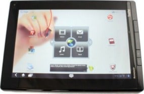
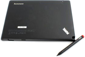
In terms of connectivity, the ThinkPad Tablet has a lot going for it. Not only does the ThinkPad Tablet have a full-size USB port, but it also offers a card reader, microUSB port, mini HDMI port, a ThinkPad Tablet dock connector, and headphone jack. Most tablets on the market today offer considerably fewer ports, so this is an area where the ThinkPad Tablet really shines.
IT departments will also appreciate the encryption and remote wipe capabilities of the ThinkPad Tablet. The optional pen accessory is definitely a nice add on that gives the tablet some additional functionality, and we found ourselves using it often during our evaluation process. The biggest drawback to this tablet is its battery managment. Assuming you’re religious about pressing the power button each time you’re finished using the tablet, it won’t be a problem. If you’re like us and tend to forget however, you’ll want to keep a charging cord nearby at all times. Regardless, we feel the ThinkPad Tablet is a great tablet for business users who want some of the added capabilities and software that Lenovo includes. It’s a full-featured device that offers a tablet experience not found in many others on the market right now.
Hot
- NVIDIA Tegra 2 dual-core 1GHz ARM SoC w/ NVIDIA graphics
- 1GB of RAM, 16 – 64GB Storage
- Lots of ports: mini HDMI, USB 2.0, micro USB, dock connector
- Full size media card reader
Not
- Relatively short battery life in idle mode
- Pen is not included (costs $30)
[Price: 16GB: $499, 32GB: $569, 64GB: $669]
Apple iPad Sales Slowing as Amazon Lights Kindle Fire [Dec 7, 2011]
Since launching in 2010, Apple’s iPad has been the global leader in tablets. But since Amazon’s first table, the all-new low-priced Kindle Fire came out in November Apple’s dominance may be sagging. In a new analyst note, Shaw Wu of the brokerage firm Stern Ageesees iPad sales as a “little light” in the current quarter.
Wu assigns the blame for light iPad sales to stiff competition, namely from Amazon’s Kindle Fire, priced at $199 while the starting price for the Apple iPad is $499. He also notes that some Apple customers are buying the MacBook Air instead of an iPad, but in lowering his estimate for iPad sales in the quarter from to 13.5 million units from 15 million units, it’s clear the Kindle Fire is the leading culprit.
[from: Apple’s iPad sales look light amid Kindle Fire, MacBook Air popularity [Dec 7, 2011]
Wu wrote in a research note:
In the Mac business, we are seeing particular strength in the MacBook Air, arguably the best ultra-mobile PC on the market. Last but not least, iPads appear a little light of expectations due in part to competition from Amazon’s Kindle Fire but also as some users opt for a more full-featured MacBook Air.]
IHS iSuppli estimates Amazon will sell nearly four million Kindle Fire tablets by the end of the year— not bad for a product that didn’t ship until mid-November. Reviewers note that the Kindle Fire isn’t the Apple iPad — it is short on apps and isn’t known for content creation abilities. Yet it seems to serve at a low price what most tablet buyers want — a handy device good for watching videos and Web browsing and content reading on the go.
It’s not like Apple’s iPad dominance is going away, either. If the company sells 13.5 million tablets in the quarter as Wu estimates, the Cupertino, Ca.-based company still has a global leader on its hands. But the Kindle Fire has shown out of the gate that a device can ably compete with the iPad after others like the HP TouchPad and the BlackBerryPlayBook failed.
Wu isn’t the only analyst who thinks the Amazon Kindle Fire is dipping into Apple iPad dominance, either. Another new report from Michael Walkley of Canaccord Genuitysees the same trend.
“With our expectations for a new iPad launch during the March quarter leading to potentially lower inventory levels combined with increased competition from the $200 Kindle Fire,” Walkley said in a note, “we have slightly lowered our December quarter iPad estimates from 14M to 13M units.”
But it’s interesting to note that some analysts don’t think Apple is overly concerned with the low-priced Kindle.
“If anything, we believe that Apple is not too concerned about the low-priced entrants,” wrote Mark Moskowitz, an analyst with J.P. Morgan, in a Dec. 2 research note. “Recall, it has been our view that low-priced, reduced feature-set entrants, such as the Kindle Fire, are soap box derby devices stuck between a tablet and an e-reader.”
iPad feeling some heat from Amazon’s Kindle Fire [Dec 1, 2011]
Apple’s iPad seems to have run into the one Android tabletthat could knock it down a peg or two.
After hitting retailers on November 15 at $199, Amazon’s Kindle Fire tablet is already outselling the iPad at Best Buy. Sorting tablets by the top sellers at the Best Buy Web Siteshows the Fire in first place followed by the 16GB Wi-Fi-only iPad 2 at $499 coming in second. A range of other iPad flavors from different carriers are scattered throughout the top 40 tablets.
Amazon itself shows the Kindle Fire as the top-selling tableton its site, with the 16GB iPad further down the list. But that seems a less accurate gauge of popularity since Fire buyers may be more likely to pick up the tablet directly from Amazon.
Even before the Fire launched a little more than two weeks ago, the tablet was proving to be a big seller, racking up a huge number of preorders. Pegging the Fire as one of the hottest consumer devices among holiday buyers, research firm DisplaySearch recently increased its shipment projectionsfor the current quarter.
DisplaySearch analyst Richard Shim now expects Amazon to ship up to 6 million Fire tablets this season, up from 4 million previously.
Another analyst also sees the Fire giving the iPad some competition, but to a lesser degree.
In an investor note out today, J.P. Morgan analyst Mark Moskowitz said he’d trimmed his fourth-quarter sales estimates for Apple’s tablet to 13 million from 13.3 million previously. Moskowitz attributed the lower forecast mostly to more limited growth in production but also pointed to the Fire.
“To a lesser extent, the Amazon Kindle Fire’s better-than-expected momentum with more price sensitive consumers is a factor, too,” the analyst wrote.
Of course, Apple is certainly in no danger of losing its current dominance in the tablet market. Moskowitz believes that over time the iPad will actually gain more traction in the business and educational markets. And despite the hot holiday demand for the Fire, the analyst doesn’t see Amazon’s current version of its tablet as a strong enough competitor over the long haul.
“We think that for any vendor to wrestle momentum longer-term from Apple, a fully loaded offering is a must, and here, the current revision of the Kindle Fire falls short,” Moskowitz wrote. “We think that, over time, consumers may come away disappointed with the Kindle Fire’s lack of functionality and smaller screen size. In our view, the Kindle Fire is the current Netbook of the media tablet market. The bigger question is whether the Fire evolves into a bona fide tablet in its next-generation release.”
As a consequence of the above two articles one observer dares to note that:
Not even Apple understands the tablet market [Dec 7, 2011]
Just last quarter, iPhone sales took a big dip. Apple (AAPL) was fine as iPads saved the day. This quarter could turn out to be the complete opposite.
If Sterne Agee analyst Shaw Wu is right, iPad sales will be lower than expected because of the popularity of both Amazon’s (AMZN) Kindle Fire table and Apple’s own MacBook Air, as ZDNet’s Larry Dignon notes. It’s a competition sandwich that underscores how little, still, anyone in the tablet market, including Apple, thoroughly understands the dynamics and what people ultimately want to do with the devices.
…
Initial trials are over
Not that the iPad — or other tablets — will whimper and crawl to a corner. Far from it. But given what products that Wu thinks are drawing attention, Kindle Fire and MacBook Air, you have to question whether anyone knows, yet, what consumers want from tablets, particularly as we’ve yet to see any solid numbers (and are unlikely to) for Kindle sales.
The presumption is that Kindle Fire snags the price-sensitive and Amazon fans. The MacBook Air switch is by people who need a lot more than what the iPad can deliver. That throws open a lot of assumptions. What percentage of buyers expected a tablet to be a media access device only? How many realized that they needed more than an on-screen keyboard? What price points will maximize sales?
For most of the Android tablet vendors, the answer to “What do consumers want?” has been, “Something other than what you sell.” Maybe Apple has all the answers, but even that seems pretty unlikely. Last quarter, unit sales were up. This month, maybe down. Steve Jobs was certain that a 7-inch tablet couldn’t see any success, but Amazon seems to be disproving that.
It’s time for everyone to take a step back and reconsider the basic questions. Maybe talk to a lot of customers, do some usability studies, and follow individuals around (with their permission) to better understand how they use the devices. Only some determined research is going to get beyond the seat-of-the-pants navigation that the tech industry seems to heartily embrace so often.
Evercore: Amazon will own 50% of Android tablet market in ’12 [Dec 5, 2011]
The Kindle Fire may “vaporize” the market for every for-profit tablet maker except Apple
In a note to clients Monday about Apple (AAPL), Evercore Partners’ Robert Cihra summarizes the impact of Amazon’s (AMZN) Kindle Fire on the tablet market in stark terms:
While Amazon’s Kindle Fire has come out of the gates strong, as expected, we see Apple maintaining its competitive lead, if anything accentuated by what now looks like the only tablet to so far mount any credible iPad challenge apparently needing to do so by selling at cost; not to mention Amazon’s success may just vaporize other “for profit” Android tablet OEM roadmaps (e.g., we est Amazon 50% of all Android tablets in CY12). Meanwhile Apple goes on as the only vendor able to cream off the most profitable segment of each market it targets, whether tablet, smartphone or PC. (emphasis ours)

The up-the-market case #1: Asustek sets shipment goal for 2012 [Dec 6]
Asustek Computer, at its global sales meeting on December 5, has set the shipment goals for its four major product lines for 2012 with notebooks and netbooks together to surpass 22 million units and the company internally expecting shipments to reach 23.8 million units, while tablet PCs will reach at least three million units with the company internally expecting the volume to reach six million units, surpassing Samsung Electronics.
…for tablet PCs, Asustek expects its shipments will reach about 1.8 million units in 2011.
…
As for the recent report that Asustek was not invited into the Windows on ARM (WOA) development project, Asustek noted that it has the strongest R&D ability among notebook vendors and is the largest client of Nvidia; therefore, the company will continue to have tight partnership with ARM-based processor makers over development of the WOA platform.

See also: NVIDIA Tegra 3 and ASUS Eee Pad Transformer Prime [Nov 10 – Dec 2, 2011]
for all related information + Asus Eee Pad Transformer Prime: The Rolls-Royce of Android tablets [Dec 2, 2011] as one of the first reviews
Note: Wistron Enters Asustek’s Tablet PC Supply Chain [Dec 8, 2011]
Aimed at becoming the largest brand for the Android- and Windows8-enabled tablet PCs, Asustek has aimed to challenge a goal of six million tablet PCs in 2012, three times that of this year’s 1.8 million units.
Asustek Unveils Transformer Prime Amid Aggressive Goal for Tablet Market [Dec 5, 2011]
Asustek Chief Executive Officer (CEO) Jerry Shen … vowed that his company will become one of the top tablet brands, next only to Apple (iPad) and Amazon (Kindle Fire). His pledge is considered by some industry executives as a challenge against Samsung, which is now the most popular brand name supplier of tablets only trailing Apple and Amazon.
Demo: Ice Cream Sandwich on Asus Transformer Prime [nvidia, Nov 17, 2011]
The up-the-market case #2: Acer, Lenovo to launch quad-core tablet PCs [Nov 29, 2011]
Acer and Lenovo are set to launch quad-core tablet PCs featuring Google’s Android 4.0 (Ice Cream Sandwich) and Nvidia’s Tegra 3 in the first quarterto compete against Asustek Computer, which has already launched its latest Eee Pad Transformer Prime with Tegra 3 and Samsung Electronics, according to sources from notebook players.
The sources pointed out that the competition over the quad-core tablet PCs will be difficult as these quad-core devices will only see improvements over their performance and design, but will still feature the same concept as their dual-core predecessors.
Therefore, these players may need to battle it out before being able to enter competition against players such as Amazon or Apple, the sources noted.
The sources noted that although these players’ performance in the dual-core tablet PC competition were not as good as expected, they will continue to advance and launch new quad-core devices to defend their brands.
The new quad-core tablet PCs from Acer and Lenovo are expected to be priced between US$459-599.
Since non-Apple players’ machines have no advantage to compete against Amazon or Apple’s tablet PC devices, the sources believe non-Apple players will together account for only 10-15% of the total tablet PC market.
The real up-the-market case: Amazing Screen Technology: Samsung Flexible AMOLED [Dec 4, 2012]
Some time earlier this year there were concept drawings of a Samsung phone with a flexible OLED display. This was a rather intriguing concept that we didn’t think would be happening anytime soon, but we were then proved wrong as Samsung stepped forward and said that flexible display smartphones were in the works and would be introduced some time in 2012.
Now Samsung’s Mobile Display Division has released a new concept video of what a transparent and flexible tablet of the future could look like and what it could accomplish. We’re guessing that Samsung’s flexible smartphone for 2012 won’t be anything like the concept video, but we definitely like where Samsung’s ideas are headed.
It showcases a tablet that can be shrunk and expanded according to our needs, augmented reality translation, and what appears to be 3D imagery as well that seems to literally leap off your screen.
From: Samsung shows off flexible display concept tablet in video [Dec 5, 2011]
In its quarterly earnings call, Samsung’s vice president of investor relations, Robert Yi, told investors, analysts and press, “The flexible display we are looking to introduce sometime in 2012, hopefully the earlier part. The application probably will start from the handset side.”
After flexible-screen mobile phones roll out, the company plans to introduce the same technology for tabletsand other devices.
In January 2011, Samsung purchased Liquivista, a strategic acquisition that will allow it to produce the kinds of displays that were announced today. Liquivista made electrowetting display technology, which is used to create mobile and other consumer electronic displays that are bright, low-power, flexible and transparent.
Flexible screen technology was also a focus of Samsung’s in March, when Yongsuk Choi, director of Samsung Mobile Display, gave an overview of the company’s future mobile device plans. At that time, Choi said most of the flexible-display technology Samsung was working on was still in very early stages.
From: Samsung’s new phones will have flexible screens [Oct 28, 2011]
See also on Samsung Mobile Display site:
– Future Display Used : Flexible Display – Foldable Display – Dual Display – 3D Display – Paper Thin Display: “Flexible Display: AMOLED products that are still fully functional when they are folded or rolled can be expanded and applied to full-color and mobile market as digital signage and e-book markets and technologies are developed.” …
– SMD History: … “Nov 2010: Developed WVGA [Wide VGA 800×480 resolution] Flexible AMOLED for the first time in the world” … “May 2009: Developed the world’s biggest 6.5” of Flexible AMOLED” …
HP, Dell, Acer to expand R&D investments [Nov 24, 2011]
Seeing that the PC industry is going through a slowdown, PC players Hewlett-Packard (HP), Dell and Acer have all expanded their investments in R&D and as the PC industry will enter an atmosphere that is filled with multiple platformsin 2012, each vendor’s R&D, branding and marketing abilities will become important drivers to increase their competitiveness in the future, according to sources from PC players.
HP is set to increase its investment in R&D and to strengthen the related resources. The company also changed its policy to have senior vice president of research, and director of HP Labs Prith Banerjee directly report to company CEO Meg Whitman.
Meanwhile, Dell is set to expand its R&D funding to US$1 billion each year, up 51.28% from US$661 million, that was reported a year ago. Dell also noted that the company will continue to acquire companies in the future and will need more funding to integrate the acquired firms.
Furthermore, Acer’s first R&D center is also expected to increase its total engineers from 600 in the middle of the year to 1,000 by year-end with executives of brand vendors and ODMs all major targets for headhunting.
An Acer executive also pointed out that the PC industry is experiencing a significant change, transitioning from Wintel system dominated to competition between several different platforms. Therefore, to the ability to develop devices based on Google’s Android system or ARM will become important.
AMD helping Android fans port to x86 [Dec 6, 2011]
A team of developers working privately to port the next version of Android to the x86 platform has been receiving a lot of support from AMD, but less from other key players.
The project is seeking to port the Ice Cream Sandwich (ICS) android-4.0.1_r1 release build to the x86 platform, and Chih-Wei Huang, one of the enthusiasts involved, told The Register that AMD had not only donated two tablets to the cause, but also has a couple of engineers helping out. As a result, the porting to AMD’s Brazos platform is now largely complete and the source code has been made available.
The first porting of Android to the x86 platform was actually done by Google engineers, but he explained that the Google team had not been continuing with the project since Android version 1.5, aka Cupcake. While the developers submit patches to Google, they seldom hear back, although some Google engineers are helping out privately with the project. Intel, too, hasn’t been keen.
“Generally speaking, Google didn’t care for the x86, at least before ICS,” he told The Registerin an email conversation. “Intel doesn’t care, either. They don’t want to help us. I’ve tried to contact Intel in different ways, but the replies were negative.”
Intel’s position has caused the team considerable problems, not least in getting Android to work with the video chipsets, and particularly the hardware acceleration added to Chipzilla’s kit. Work is still continuing, but since this is a voluntary project by people who have day jobs, then Android users might have a while before they can plaster an Intel Inside sticker on their systems.
Chih-Wei Huang, an open source advocate based in Taiwan, started the project with a former colleague in June 2009, and it has morphed to the point where the scheme has 2,600 subscribers to the project forum. He said that while he tried to keep the porting process up to date, it was a lot of work and some people weren’t sharing data.
“Now ICS is more mature for x86 tablet or netbook, so there are more practical reasons to do that,” he said. “Actually, I know some vendors like Bluestack, Viewsonic, and Insyde have already shipped Android-x86.org based products. However, they never contribute back. That usually makes us feel bad and angry.”
Supplementary information: Android: A visual history [Dec 7, 2011]
