
The growing popularity of visual applications for displaying increasingly rich data sets is clearly a key driver behind the rising momentum of Android among embedded developers. Industrial Automation (28%), Infotainment (20%), and Digital Signage (12%) were the top three applications in the survey, closely followed by HMI (11%) and Medical (11%).
The ability to add a touch interface (26%) was listed by respondents as the main benefit of adopting Android, with reduced time to market (25%) and customizability (19%) coming in second and third respectively. Native multimedia support (14%) in the O/S and the robust Android app ecosystem (12%) were also seen as important.
As a mobile O/S, Android does offer some critical challenges for developers to overcome when implementing it for embedded applications, including its lack of I/O support for peripherals (23%), the need to maintain different versions of it, and ensuring security (17%). Building up internal Android development expertise (21%) and finding the right development tools (19%) are other key issues embedded developers face in adopting the O/S.
We’d like to thank everyone who responded to the survey for the invaluable feedback they provided. We have already begun analyzing the results in order to determine how we can improve the platforms and services we offer for Embedded Android, and will be updating you on our progress.
Download the full results here.
Home » Posts tagged '28nm'
Tag Archives: 28nm
Embedded Android — A VIA Technologies Strategic Direction in addition to its earlier joint CPU venture with the Shanghai government
– Nov 12, 2012 – July 11, 2014: Can VIA Technologies save the mobile computing future of the x86 (x64) legacy platform? for preliminary reading on this blog
– October 8, 2014: Coming very soon from Centaur Technology: A Leap Ahead in Chip Design as a very small glimpse into the next generation by the Centaur Technology
– October 13, 2014: Centaur Technology: Do the same job that an Intel processor can do, but doing it less expensively, with a much smaller group and Glenn Henry in charge as another as a very small glimpse …
June 3, 2015: VIA pushing for profitability in 2015 by DIGITIMES
VIA Technologies [威盛電子] president Chen Wen-Chi [陳文琦 the spouse of Cher Wang Chairwoman and CEO of HTC] has maintained that the company will not be delisted from the Taiwan Stock Exchange (TSE) and will have a good chance of turning profitable in 2015. [http://technews.tw/2015/06/02/via-technologies-condition/: “this year the operation has turned the corner, there is the opportunity to turn profit, but not sure“]
Chen said during a shareholders meeting on June 2 that VIA’s revenue performance became stable in 2014, while losses have also started narrowing. With its embedded platform and digital signage businesses starting to contribute profits, VIA is expecting an optimistic result for 2015.
As for the recent market rumor about Intel considering acquiring its subsidiary GenieNetworks[a CDMA licensing business having 2 clients by the end of 2014], Chen declined to comment.
December 29, 2014: Ownership of the Centaur Technology has been transfered to VIA CPU PLATFORM, INC. established on December 17, 2013 (⇒威盛電子:代子公司VIA USA Inc.公告進行美國子公司Centaur Technology Inc.股權之投資架構調整) and whose president is Timothy Chen (陳主望), Cher Wang’s nephew
December 25, 2014: VIA to return to profitability in 2015, says company president by DIGITIMES
… As for the China government’s recently announced strategy to fully support and nurture local semiconductor players, Chen believes it could bring a strong challenge to the Taiwan and worldwide semiconductor industries, but VIA has been forming partnerships with China’s players and will only see limited impact from the policies.
November 21, 2014: VIA stock demoted in TSE; expects strong performance in 4Q14 by DIGITIMES
VIA Technologies has recently been demoted to become a full-cash delivery stock by the Taiwan Stock Exchange (TSE) because its stock’s net asset value dropped below NT$5 (US$0.16) in the third quarter. Commenting on the incident, special [technical] assistant to the president [also Head of Sales and Marketing since 1996 according to LinkedIn and VP Business Development and Strategy, VIA Technologies, HTC according to
World Economic Forum 2015], Timothy Chen pointed out that the company had losses in the third quarter because its embedded solution orders were delayed and it had non-recurring engineering (NRE) expenses.
…
Although VIA’s CPU business continues to suffer from losses, the company’s invested Wondermedia [in 2014 focused on ARM-based tablet and STB processor development], VIA Labs [having USB 3.0 chips already for the 2014 market] and GenieNetworks as well as the joint venture with the government of Shanghai, China still contribute income.
…
Chen noted that VIA has not yet given up the x86 CPU market and its licensing agreement with Intel is valid until 2018. Although VIA did not achieve much performance in the PC market, the company is seeing stable orders for embedded applications such as digital signage.The company’s joint venture with the Shanghai government is currently developing x86-based processors and 3D graphics chips and should help the company return to the PC market in the second half of 2015. The joint venture has R&D centers in Shanghai, Beijing and Wuhan, China and has about 600 employees currently.
February 19, 2014: VIA reportedly moving x86 CPU resources to new joint venture in China by DIGITIMES
VIA Technologies is rumored to have started shifting its x86 CPU technologies and related personnel to its newly formed IC design joint venture with a China government-owned investment firm, according to market watchers
…
The joint venture was announced in early 2014 with VIA owning a 20% stake in the company.
…
Because VIA’s x86 CPU business is licensed by Intel, moving related resources to a new joint venture is expected to attract Intel’s attention. However, the chip giant may not be able to do much because Intel reached an agreement with the US’s Fair Trade Commission (FTC) in 2010 to not interfere with competition in the CPU and chipset markets, and extend its licensing of PCI Express to VIA by at least another six years. Intel is also unlikely to wish to offend the China investment firm, which has support from the China government, the market watchers analyzed.
VIA Alliance Semiconductor Co., Ltd. > Introduction:
VIA Alliance Semiconductor Co., Ltd. [磐聚网] was established in April 2013 with a total registered capital of USD$250M. As a joint venture between Shanghai Alliance Investment Ltd. [SAIL] who is affiliated to Shanghai SASAC and VIA Technologies, Inc., VIA Alliance Semiconductor Co., Ltd. has about 1000 employees and locates its headquarter at Zhangjiang of Shanghai with branches in Beijing, Hangzhou, Wuhan, Shenzhen, Taiwan, California and Texas of America.
With the forefront technologies and know-how in the design of CPU, GPU and chipsets, VIA Alliance Semiconductor Co., Ltd. is well known to provide high security, high performance, low power dissipation, and low cost SoC solutions.
As a fabless SoC factory, VIA Alliance Semiconductor Co., Ltd. adopts advanced 40nm and 28nm semiconductor processes. VIA Alliance Semiconductor Co., Ltd.’s main products include CPU and chipsets for desktop PC and laptop and ARM Cortex series SoC with its state of the art Elite series GPU and Video Engine IPs. VIA Alliance Semiconductor Co., Ltd. aims at becoming the leading SoC solution supplier for smart TV, smart phone and enterprise
January 17, 2013: VIA forms IC joint venture with Shanghai Alliance Investment by DIGITIMES
VIA Technologies has announced that it has set up an IC design house jointly with Shanghai Alliance Investment Company targeting the growing chip market in China.
The joint venture will be capitalized at US$250 million with Shanghai Alliance Investment contributing 80.1% of total capital, while VIA makes up the remaining 19.9%. An initial investment of US$100 million is slated for completion by the end of March 2013, VIA said.
VIA posted revenues of NT$3.36 billion (US$115.47 million) for 2012, decreasing 20.8% from a year earlier.
September 2014: Research and development of Lenovo M6000/S6000 desktops with ZX-A C4350AL [VIA Nano X2 announced on January 4, 2011] CPU have been completed
November 2014: Mass production of Great Wall desktops using ZX-A C3450AL total solution have been achieved
– Targeting a range of Desktop products ZX-A processors and V11PH solution extend the reach into multitasking and performance-oriented segments and offer end users an optimal, power-efficient computing experience
– ZX-A processors are built using the latest 40nm fabrication process. ZX-A processors’ package size is 21mm x 21mm and the die size is only 11mm x 6mm. The launched processor name is C4350AL (the Clock Speed is 1.6G+).
– ZX-A processors are x86 architecture CPUs, support 32-bit/64-bit and the extended instruction sets. ZX-A are the first truly optimized, low power dual-core processors delivering industry leading performance-per-watt and improved multi-tasking ability, without consuming more power. ZX-A processors leverage a multi-core architecture to offer up to twice the performance in multi-thread optimized applications, while staying within the same signature low-power envelope.
– Featuring two out-of-order x86 cores, ZX-A processors come with native 64-bit software support, VT CPU virtualization technology, and PadLock hardware security features.
– Targeting a range of Mobile Notebook products ZX-A processors and VX11H solution extend the reach into multitasking and performance-oriented segments and offer end users an optimal, power-efficient computing experience
– ZX-A processors are built using the latest 40nm fabrication process. ZX-A processors’ package size is 21mm x 21mm and the die size is only 11mm x 6mm. The launched processor name is C4350AL (the Clock Speed is 1.6G+).
– ZX-A processors are x86 architecture CPUs, support 32-bit/64-bit and the extended instruction sets. ZX-A are the first truly optimized, low power dual-core processors delivering industry leading performance-per-watt and improved multi-tasking ability, without consuming more power. ZX-A processors leverage a multi-core architecture to offer up to twice the performance in multi-thread optimized applications, while staying within the same signature low-power envelope.
– Featuring two out-of-order x86 cores, ZX-A processors come with native 64-bit software support, VT CPU virtualization technology, and PadLock hardware security features.
– ZX-C series processor is a new generation of quad-core processors, they are designed for high-performance computing
– ZX-C processors are built using the latest 28nm fabrication process. ZX-C processors’ package size is 21mm x 21mm and pin to pin match with ZX-A.
– There are 4 CPU cores integrated on the single chip packaging. Delivering industry leading performance per watt and improved multi-tasking ability, without consuming more power. ZX-C processors leverage a multi-core architecture to offer up to quad the performance in multi-thread optimized applications, while staying within the same signature low-power envelope.
– Featuring four out-of-order x86 cores, ZX-C processors come with native 64-bit software support, VT CPU virtualization technology, and hardware security features.
– VX11PH Chipset offering a world-class HD multimedia platform for media-intensive applications
Already visible in July through benchmarks the next stepping of the legacy Isiah line: CentaurHauls Family 6 Model 15 Stepping 14 ⇒ VIA Technology Inc. VT3456 6628AMB, VIA QuadCore @ 2.00 GHz 2 processors, 8 cores
So the once influential VIA Technologies is desparately trying to regain its stance by capitalising on the technological fruits of the smartphone revolution which has already ended by Qualcomm’s alignment with latest developments in China via downsizing, Allwinner and Microsoft collaboration.
There are two lines of strategic actions for VIA which have become public as such recently:
1. May 20, 2015: VIA Smart ETK For Embedded Android
The VIA Smart ETK for Android provides an application programming interface (API) that simplifies Android system development on VIA Embedded ARM platforms by enabling the Android application to access I/O and manageability services provided by the system hardware that are not supported in the Android framework. These APIs help safeguard against system crashes and provide the ability to schedule auto power on and off, as well as periodic system reboots to ensure maximum performance.
The VIA Smart ETK for Android is also bundled with Smart ETK Demo, which is easy to install and has a user-friendly GUI for demonstrating the functions of VIA Embedded ARM platforms. Both the VIA Smart ETK and Smart ETK Demo are easy-to-use tools that help to shorten development time and speed up time to market. Key features include the following:
Watchdog:
This provides an API which allows the user to set a timer to ensure proper operation and help the applications/system to recover from a dead circle or breakdown. When it is set, the system will automatically reboot if no “feeding dog” signal is received.System Power Off / Reboot:
This provides APIs that allow the user to use an Android application to schedule when the system should power off as well as set periodic reboots to ensure maximum performance is maintained.RTC Wake-Up:
This provides an auto power on feature by setting the Remote Time Clock (RTC) auto wake-up timer. The RTC supports three auto wake-up modes:
Wake-up on a specified hour and minute every day
Wake-up on a specified day/ hour/ minute every week
Wake-up on a specified day/ hour/ minute every month
Legacy I/O Support:
The VIA Smart ETK enables legacy I/O support such as RS-232, by opening up GPIO, I2C, and CAN bus ports to the application.
February 26, 2015: VIA SMART ETK for Android post on VIA News by Richard Brown VP of International Marketing
We’ve seen a tremendous amount of interest in the VIA SMART ETK at Embedded World this week, particularly for embedded Android system design applications.
As its name implies, the VIA SMART ETK is an embedded tool kit that we offer as part of our software engineering services in order to facilitate the development of embedded systems and devices on based on our ARM and x86 platforms.
The VIA SMART ETK for Android is available with the VIA VAB-600, VIA VAB-820, and VIA VAB-1000 boards, as well as the VIA ALTA DS, VIA ALTA DS 2, VIA ARTiGO A900, and VIA Viega systems. It provides an application programming interface (API) that simplifies Android system development by enabling the Android application to access I/O and manageability services provided by the system hardware that are not supported in the Android framework. These APIs help safeguard against system crashes and provide the ability to schedule auto power on and off, as well as periodic system reboots to ensure maximum performance.
One of the key features we have enabled in the VIA SMART ETK for Android is support for legacy I/O such as RS-232 by opening up the GPIO, I2C, and CAN bus ports to the application. Others include Watchdog, System Power Off/Reboot, and RTC Wake-Up. To learn more, please visit the ARM Software Engineering Services page on our website and download our white paper “Cracking the Embedded Android Code” [January 26, 2015].
We are committed to the continued long-term development of the VIA SMART ETK for Android and regularly issue new releases of it for the boards and systems listed above. Watch this space for news of the latest updates.
2. [February 5, 2015⇒Android-Based Digital Signage Solutions] Signage Solution Pack for Android as the first of software solution packs optimized to meet the requirements of specific vertical market segments
The Signage Starter Solution Pack for Android has been designed to accelerate the development of digital signage solutions using the VIA ALTA DS and VIA ALTA DS 2 [Oct 15, 2014 ⇒ the Solution Pack already came with ⇒Android Signage Goes Dual Screen with VIA ALTA DS 2] systems. It includes a number of APIs that help safeguard against system crashes provide the ability to schedule auto power on and off as well as periodic system reboots to ensure maximum performance, unique to Android OS for digital signage applications. Key features include:
Watch Dog:
Provides an API which allows the user to set a timer to ensure proper operation and help applications/system to recover from a dead circle or breakdown. When it is set, the system will automatically reboot if no “feeding dog” signal is received.System Power Off / Reboot:
Provides APIs which allow the user to use an Android application to schedule when the system should power off as well as set periodical reboots to ensure maximum performance is maintained.RTC Wake-Up:
Provides an auto power on feature by setting Remote Time Clock (RTC) auto wake-up timer. The RTC supports three auto wake-up modes:
Wake-up on a specified hour and minute every day
Wake-up on a specified day/ hour/ minute every week
Wake-up on a specified day/ hour/ minute every month
Customer ID:
Provides a unique ID which matches the software to a particular VIA ALTA DS system helping to protect the customer’s application or to identify a particular system.
July 9, 2015: Embedded Android Survey – The Results Are In! by Michael Fox of VIA Technologies


As the enhancement of the technology portfolio there is the new
The VIA HD Video Monitoring Starter Kit is a turnkey solution aimed at accelerating the development of wireless multi-node video monitoring systems for the rapidly growing home and commercial markets.The starter kit includes:
- VIA ALTA DS 2 System
- Customized Android BSP & VIA Smart ETK
- VIA Video Management Software
- 4 Wireless IP Cameras
VIA ALTA DS 2 System
At the heart of the starter kit is the ultra-compact fanless VIA ALTA DS 2 system. Powered by a 1.0GHz dual core VIA Elite E1000 Cortex-A9 SoC with a high-performance 2D/3D graphics and video engine that supports Open GL ES 3.0 hardware acceleration and simultaneous multiple Full HD video playback. The VIA ALTA DS 2 includes SATA and Micro SD Card support, allowing recorded footage to be stored locally for playback at a later time or offloaded to the cloud.
Customized Android BSP & Smart ETK
Included with the ALTA DS 2 system is an Android BSP (Board Support Package) customized for video monitoring applications which includes the following enhancements:
- Storage – performance improvement
- Hardware enabled decoding
- RTSP & WVTP parse performance improvement
- Hardware acceleration for on screen preview playback
To enable customers to shorten their development time and speed time to market for their specific application needs, the starter kit also includes the VIA Smart ETK (Embedded Tool Kit), which provides a set of APIs for applications to access I/O and manageability services provided by the system hardware.
VIA Video Management Software (VMS)
VIA VMS application framework provides basic functionality including HD playback support, hardware accelerated decoding for live streaming and local/network backup support.Video Streaming & Recording Performance
Live Stream: (Channels/Resolution/Bitrate) Playback Frame Rate/Stream Recording Performance 1ch 1080p @ 8Mbps 30fps 1Ch 1080p @8Mbps 4ch 720p @ 4Mbps 30fps 4Ch 1080p @8Mbps Live Playback Layouts
Wireless IP Cameras
The starter kit includes 4 validated IP cameras featuring OmniVision’s OV9712 CameraChip™ sensor, developed with their proprietary OmniPixel3-HS™ high sensitivity pixel technology to provide excellent scene reproduction in both extremely high and low-light environments, and their OV788 video signal processor for video compression, 720p HD video streaming, and AES-256 encryption over any Wi-Fi network, the system offers ‘instant-on’ crisp HD video and streaming capabilities in an extremely power-efficient, battery operated package.


Which is related to the
April 8, 2015: OmniVision and VIA Announce Partnership to Develop Battery-Powered Wireless HD Video Monitoring Solution news release as well
Customizable Android™ Based Reference Design to Accelerate Time to Market, Optimize Home and Small Business Monitoring Systems
SANTA CLARA, Calif., April 6, 2015 — OmniVision Technologies Inc. (NASDAQ: OVTI), a leading developer of advanced digital imaging solutions, and VIA Technologies, Inc., a leader in embedded IoT and M2M platform innovation, today announced a partnership to develop a battery-powered high definition (HD) video monitoring solution that enables OEMs to dramatically reduce time-to-market for wireless multi-node monitoring systems in homes and small businesses.
“This partnership between OmniVision and VIA Technologies exemplifies both companies’ desire to meet the rapidly growing demand for turnkey solutions that can give OEMs the ability to quickly and cost-effectively bring innovative smart devices to market,” said Paul Gallagher, senior director of marketing at OmniVision. “By offering ‘instant-on’ crisp HD video and streaming capabilities in an extremely power-efficient, battery operated package, OmniVision’s OV9712 and OV788 video signal processor together provide excellent capabilities for the advanced solution now under development.”
“By combining OmniVision’s industry-leading imaging technologies with VIA’s advanced video processing technologies and embedded Android system design capabilities, we have produced a highly competitive turnkey solution,” said Epan Wu, head of VIA Embedded. “We look forward to collaborating with OmniVision and driving the development of new and innovative technologies for the rapidly growing market for home and commercial monitoring systems.”
Utilizing the OV9712 CameraChip™ sensor developed with OmniVision’s proprietary OmniPixel3-HS™ high sensitivity pixel technology, the solution will be designed to achieve excellent scene reproduction in both extremely high- and low-light environments. The OV9712 will operate in conjunction with OmniVision’s ultra-low power OV788 video signal processor. That processor will provide video compression, 720p HD video streaming, and AES-256 encryption over any Wi-Fi network, thus allowing users to quickly stream high quality video content using the video monitoring solution.
About OmniVision
OmniVision Technologies (NASDAQ: OVTI) is a leading developer of advanced digital imaging solutions. Its award-winning CMOS imaging technology enables superior image quality in many of today’s consumer and commercial applications, including mobile phones, notebooks, tablets and webcams, digital still and video cameras, security and surveillance, entertainment devices, automotive and medical imaging systems. Find out more at: www.ovt.com
Cortex-A53 is used alone in higher and higher-end devices as the result of increased competition between MediaTek and Qualcomm

We’ve learned a lot during the last one a half years about the superiority of the Cortex-A53 cores for the mass produced SoCs. Some major points about that you see on the right:
My prediction back in Dec 23, 2013 was that The Cortex-A53 as the Cortex-A7 replacement core is succeeding as a sweet-spot IP for various 64-bit high-volume market SoCs to be delivered from H2 CY14 on. Such a prediction is a reality now as no less than 291 smartphones are listed as of today in PDAdb.net, which are using the Qualcomm Snapdragon 410 MSM8916 quad-core SoC based on Cortex-A53. The first such device, the Lenovo A805e Dual SIM TD-LTE was released in July, 2014.
Meanwhile Qualcomm’s downstream rival, MediaTek is moving up fast with its offerings as well. There are 8 devices based on quadcore MT6732M since Dec’14, 27 devices which based on quad-core MT6732 since Nov’14, and even 6 devices based on octa-core MT6753 since Jan’15. Note however that there are 3 such products from the Chinese brand Meizu, and one each from another local brands, Elephone and Cherry Mobile. Only the ZTE model is from a 1st tier global vendor yet.
My prediction was also proven by the fact that interest in that post was the highest on this blog as soon as the respective new SoCs, and commercial devices based on them arrived:

Now even higher end, octa-core smartphones based on Cortex-A53 alone are coming to the market from 1st tier device vendors
June 1, 2015: Asus ZenFone Selfie (ZD551KL)
(launched on the ASUS Zensation Press Event at Computex 2015)
from the product site:
ZenFone Selfie features the industry’s first octa-core, 64-bit processor — Qualcomm’s Snapdragon 615. With its superb performance and superior power-efficiency you’ll shoot sharp photographs at stupefying speed, record and edit Full HD (1080p) video with minimal battery draw, and enjoy using the integrated 4G/LTE to share everything you do at incredible speeds of up to 150Mbit/s!
expected price in India: ₹12,999 ($205)
(Re: “coming in an incredible price” said in the launch video about the earlier ZenFone 2 (ZE551ML) which has the same price, but a 1.8 GHz Intel Atom Z3560 processor, only 5 MP secondary camera etc.)
from the ASUS Presents Zensation at Computex 2015 press release:
ZenFone Selfie is a unique smartphone designed to capture the best possible selfies, quickly and simply. Featuring front and rear 13MP PixelMaster cameras with dual-color, dual LED Real Tone flash, ZenFone Selfie captures beautiful, natural-looking selfies in gloriously high resolution. The rear camera features a large f/2.0 aperture lens and laser auto-focus technology to ensure near-instant focusing for clear, sharp pictures — even in low-light conditions where traditional cameras struggle.
ZenFone Selfie includes the brilliant ZenUI Beautification mode for live digital cosmetics. A few taps is all that’s needed to soften facial features, slim cheeks, and enhance skin tone to add vibrancy, and all in real time — injecting instant verve into any composition. ZenFone Selfie also has Selfie Panorama mode, which exploits ZenFone Selfie’s f/2.2-aperture front lens and 88-degree field of view to capture panoramic selfies of up to 140 degrees. With Selfie Panorama mode enabled, selfies become a party with all friends included — plus the ability to capture panoramic scenery for stunning backdrops.
ZenFone Selfie has a large 5.5-inch screen that fits in a body that’s a similar size to that of most 5-inch smartphones, for a maximized viewing experience in a compact body that fits comfortably in the hand. It has a high-resolution 1920 x 1080 Full HD IPS display with a wide 178-degree viewing angle and staggering 403ppi pixel density that renders every image in eye-delighting detail. ASUS TruVivid technology brings color to life in brilliant clarity, making selfies and other photos look their best. Tough Corning® Gorilla® Glass 4 covers the display to help protect against scratches and drops.
ZenFone Selfie features the industry’s first octa-core, 64-bit processor for the perfect balance of multimedia performance and battery efficiency — the Qualcomm® Snapdragon™ 615. This extraordinarily powerful chip equips ZenFone Selfie to provide the very best multimedia and entertainment experiences, carefully balancing high performance with superior power-efficiency.
June 19, 2015 by SamMobile: Samsung’s first smartphones with front-facing LED flash, Galaxy J5 and Galaxy J7, now official
Samsung has announced its first smartphones with a front-facing LED flash; the Galaxy J5 and the Galaxy J7. Specifications of these devices were previously leaked through TENAA, and their UI was revealed through Samsung’s own manuals. Now, they have been officially announced in China, where they would be available starting this week, but there’s no clarity about their international launch.
All the mid-range and high-end smartphones from the company released recently have started featuring high-resolution front-facing cameras, and the same is the case with the Galaxy J7 and the Galaxy J5. To complement their 5-megapixel wide-engle front-facing cameras, they are equipped with a front-facing single-LED flash. Other features include a 13-megapixel primary camera with an aperture of f/1.9, 1.5GB RAM, 16GB internal storage, a microSD card slot, dual-SIM card slot, and LTE connectivity. Both these smartphones run Android 5.1 Lollipop with a new UI that is similar to that of the Galaxy S6 and the S6 edge.
The Galaxy J7 is equipped with a 5.5-inch HD display, a 64-bit octa-core Snapdragon 615 processor, a 3,000 mAh battery, and is priced at 1,798 CNY (~ $289). The Galaxy J5 features a slightly smaller 5-inch HD display, a 64-bit quad-core Snapdragon 410 processor, a 2,600 mAh battery, and is priced at 1,398 CNY (~ $225). Both of them will be available in China in three colors; gold, white, and black.
The Galaxy J5 and J7 are targeted at the youth and compete with devices like the HTC Desire EYE, Sony Xperia C4, and the Asus ZenFone Selfie, all of which have high-resolution front-facing cameras with an LED flash.
May 6, 2015: Sony launches next generation “selfie smartphone” – Xperia™ C4 and Xperia C4 Dual
The selfie phenomenon is about to kick up a notch with the introduction of Xperia™ C4 and Xperia C4 Dual – Sony’s next generation PROselfie smartphones, featuring a best in class 5MP front camera, a Full HD display and superior performance.
“Following the success of Xperia C3, we are proud to introduce Sony’s evolved PROselfie smartphone,” said Tony McNulty, Vice-President, Value Category Business Management at Sony Mobile Communications. “Xperia C4 caters to consumers that want a smartphone that not only takes great photos, but also packs a punch. Benefiting from Sony’s camera expertise, the 5MP front-facing camera with wide-angle lens lets you capture perfect selfies, while its quality display and performance features provide an all-round advanced smartphone experience.”
We all like a high-profile selfie – so go ahead and get snapping:
You can now stage the perfect selfie, getting everything – and everyone – in shot, thanks to the powerful 5MP front camera with 25mm wide-angle lens. Sony’s Exmor RTM for mobile sensor, soft LED flash and HDR features means the pictures will always be stunning, even in those ‘hard to perfect’ low light conditions. Superior auto automatically optimises settings to give you the best possible picture and SteadyShot™ technology compensates for any camera shake.
With 13MP, autofocus and HDR packed in there is no compromise on the rear camera, which delivers great shots for those rare moments you’re not in the picture.
You will also be able to get even more fun out of your smartphone with a suite of creative camera apps such as Style portrait with styles including ‘vampire’ and ‘mystery’ to add a unique edge to your selfie. Moreover, apps such as AR maskgive your selfie a twist by letting you place a different face over your own face or others’ faces while you snap a selfie.
Experience your entertainment in Full HD
Now you can enjoy every picture and every video in detail with Xperia C4’s 5.5” Full HD display. Watching movies on your smartphone is more enjoyable thanks to Sony’s TV technology – such as Mobile BRAVIA® Engine 2 and super vivid-mode – which offers amazing clarity and colour brightness. Enjoy viewing from any angle with IPS technology.Great video deserves great audio to match, so Xperia C4 features Sony’s audio expertise to deliver crisp and clear audio quality. With or without headphones, you can sit back and enjoy your favourite entertainment in all its glory.
The design of Xperia C4 has also been crafted with precise detail and care to ensure every aspect amplifies the sharp and vivid display. A minimal frame around the scratch-resistant screen enhances both the viewing experience and the smartphone design, while its lightweight build feels comfortable in the hand. Xperia C4 comes in a choice of white, black and a vibrant mint.
Superior performance, with a power-packed battery that just keeps going
Whether you’re running multiple apps, checking Facebook, snapping selfies or listening to the best music – you can do it all at lighting speed thanks to Xperia C4’s impressive Octa-core processor. Powered by an efficient 64-bit Octa-core processor [Mediatek MT6752], Xperia C4 makes it easier than ever to multitask and switch between your favourite apps, without affecting performance. Ultra-fast connectivity with 4G capabilities means it’s quicker than ever to download your favourite audio or video content and surf the web without lag.
The large battery (2,600mAh) provides over eight hours of video viewing time, meaning that the entire first season of Breaking Bad can be binged uninterrupted, while Battery STAMINA Mode 5.0 ensures you have complete control over how your battery is used.
Xperia C4 is compatible with more than 195 Sony NFC-enabled devices including SmartBand Talk (SWR30) and Stereo Bluetooth® Headset (SBH60). You can also customise the smartphone with the protective desk-stand SCR38 Cover or with a full range of original Made for Xperia covers.
Xperia C4 will be available in Single SIM and Dual SIM in select markets from the beginning of June 2015.
For the full product specifications, please visit: http://www.sonymobile.com/global-en/products/phones/xperia-c4/specifications/
price in India: ₹25,499 ($400) and ₹25,899 ($408) for the Dual-SIM version
June 1, 2015: The stakes have been raised even higher by a higher-end octa-core SoC from MediaTek with 2GHz cores which is also 30% more energy efficient because of the first time use of 28HPC+ technology of TSMC
MediaTek Expands its Flagship MediaTek Helio™ Processor Family with the P Series, Offering Premium Performance for Super Slim Designs
P-series the first to use TSMC’s 28nm HPC+ process, which reduces processor power consumption
MediaTek, a leader in power-efficient, System-on-Chip (SoC) mobile device technology solutions, today announces the launch of the MediaTek Helio™ P10, a high-performance, high-value SoC focused on the growing demand for slim form-factor smart phones that provide premium, flagship features. The Helio P10 showcases a 2 GHz, True Octa-core 64-bit Cortex-A53 CPU and a 700MHz, Dual-core 64-bit Mali-T860 GPU. The Helio P10 will be available Q3 2015 and is expected to be in consumer products in late 2015.
The P10 is the first chip in the new Helio P family, a series which aims to integrate into a high-value chipset, premium features such as high-performance modem technology; the world’s first TrueBright ISP engine for ultra-sensitive RWWB; and, MiraVision™ 2.0, for top-tier display experiences. The features available in the P series include several of MediaTek’s premier technologies, such as WorldMode LTE Cat-6, supporting 2×20 carrier aggregation with 300/50Mbps data speed; MediaTek’s advanced task scheduling algorithm, CorePilot®, which optimizes the P10’s heterogeneous computing architecture by sending workloads to the most suitable computing device – CPU, GPU, or both; and, MediaTek’s Visual Processing Application – Non-contact Heart Rate Monitoring, which uses only a smartphone’s video camera to take a heart rate reading and is as accurate as pulse oximeters/portable ECG monitoring devices.
“The P series will provide OEM smartphone makers with greater design flexibility to meet consumer demands for slim form-factors, which provide dynamic multimedia experiences,” said Jeffrey Ju, Senior Vice President of MediaTek. “The P10 enables state-of-the-art mobile computing and multimedia features all while balancing performance and battery life.”
The Helio P10 is the first product to use TSMC’s 28nm HPC+ process, which allows for reduced processor power consumption. With the help of the latest 28HPC+ process and numerous architecture and circuit design optimizations, the Helio P10 can save up to 30% more power (depending of usage scenarios), compared to existing smartphone SoCs manufactured using the 28 HPC process.
“We are pleased to see MediaTek’s achievement in producing the world’s leading 28HPC+ smartphone chip,” said Dr. BJ Woo, Vice President, Business Development, TSMC. “As an enhanced version of TSMC’s 28HPC process, 28HPC+ promises 15% better speed at fixed power or 50% leakage reduction at the same speed over 28HPC. Through our competitive 28HPC+ technology and process-design collaboration with MediaTek, we believe MediaTek will deliver a series of products which benefit smartphone users across the world.”
As with the entire line of Helio SoCs, the P10 is packed with premium multimedia features. With a concentration on advanced display technologies, premium camera features, and HiFi audio, the P10 delivers leading functionality around the features most used on today’s mobile phones:
21MP premium camera with the world’s first TrueBright ISP engine:
Enables ultra-sensitive RWWB sensor to capture twice as much light as traditional RGB sensors in order to retain true color and detail, even in low light. The RWWB sensor also enhances the color resolution, even when compared with RGBW sensors.
Other features include a new de-noise/de-mosaic HW, PDAF, video iHDR, dual main camera, less than 200ms shot-to shot delay, and video face beautify.
Hi-fidelity, hi-clarity audio achieves 110dB SNR & -95dB THD
Full HD display at 60FPS with MediaTek’s suite of MiraVision 2.0 display technologies:
UltraDimming – Dimmer background lighting for more comfortable reading, even in low-light situations.
BluLight Defender – A built-in blue light filter that saves more power than conventional software applications.
Adaptive Picture Quality – Ensures the best picture quality when using different applications. True-to-life colors when in camera preview; vibrant colors when watching videos.
The MediaTek Helio P10 will be released in Q3 2015 and is expected to be available in consumer products in late 2015.
Note that Helio P1 is a significant step in MediaTek’s strategy already outlined in the following posts of mine:
– March 4, 2014: MediaTek is repositioning itself with the new MT6732 and MT6752 SoCs for the “super-mid market” just being born, plus new wearable technologies for wPANs and IoT are added for the new premium MT6595 SoC
– March 10, 2015: MediaTek’s next 10 years’ strategy for devices, wearables and IoT
AMD’s Heterogeneous System Architecture (HSA) and Graphics Core Next (GCN) is coming to notebooks
Why AMDers are excited about “Kaveri” [AMD YouTube channel, Jan 15, 2014]
The GCN architecture that is behind Xbox One and Sony PS4 (among others) and the HSA (quite probably available as well in Xbox One and PS4) are coming now to notebook APUs.
OR how much could AMD reap the benefits (first time) of ATI acquisition in 2006?
OR how much the 28nm SHP (Super High Performance) process from Global Foundries will help AMD to compete?
OR will the next-gen Steamroller microarchitecture be sufficient to compete?
How “Kaveri” is Going to Change the World of Compute Capabilities [AMD YouTube channel, Jan 16, 2014]
If it can game, imagine what else it can do. [AMD YouTube channel, Jan 6, 2014]
The Four Technologies that make up AMD’s Kaveri APU [AMD YouTube channel, Jan 14, 2014]
In AMD Kaveri Review: A8-7600 and A10-7850K Tested [AnandTech, Jan 14, 2014] it was touted as:
The first major component launch of 2014 falls at the feet of AMD and the next iteration of its APU platform, Kaveri. Kaveri has been the aim for AMD for several years, it’s actually the whole reason the company bought ATI back in 2006. As a result many different prongs of AMD’s platform come together: HSA, hUMA, offloading compute, unifying GPU architectures, developing a software ecosystem around HSA and a scalable architecture. This is, on paper at least, a strong indicator of where the PC processor market is heading in the mainstream segment.
…
My insert: AMD Kaveri APU Tech Day at CES [on Jan 5, 2014] [AMD YouTube channel, Jan 14, 2014]
End of my insert
Final Words
As with all previous AMD APU launches, we’re going to have to break this one down into three parts: CPU, the promise of HSA and GPU.
In a vacuum where all that’s available are other AMD parts, Kaveri and its Steamroller cores actually look pretty good. At identical frequencies there’s a healthy increase in IPC, and AMD has worked very hard to move its Bulldozer family down to a substantially lower TDP. While Trinity/Richland were happy shipping at 100W, Kaveri is clearly optimized for a much more modern TDP. Performance gains at lower TDPs (45/65W) are significant. In nearly all of our GPU tests, a 45W Kaveri ends up delivering very similar gaming performance to a 100W Richland. The mainstream desktop market has clearly moved to smaller form factors and it’s very important that AMD move there as well. Kaveri does just that.
In the broader sense however, Kaveri doesn’t really change the CPU story for AMD. Steamroller comes with a good increase in IPC, but without a corresponding increase in frequency AMD fails to move the single threaded CPU performance needle. To make matters worse, Intel’s dual-core Haswell parts are priced very aggressively and actually match Kaveri’s CPU clocks. With a substantial advantage in IPC and shipping at similar frequencies, a dual-core Core i3 Haswell will deliver much better CPU performance than even the fastest Kaveri at a lower price.
The reality is quite clear by now: AMD isn’t going to solve its CPU performance issues with anything from the Bulldozer family. What we need is a replacement architecture, one that I suspect we’ll get after Excavator concludes the line in 2015.
In the past AMD has argued that for the majority of users, the CPU performance it delivers today is good enough. While true, it’s a dangerous argument to make (one that eventually ends up with you recommending an iPad or Nexus 7). I have to applaud AMD’s PR this time around as no one tried to make the argument that CPU performance was somehow irrelevant. Although we tend to keep PR critique off of AnandTech, the fact of the matter is that for every previous APU launch AMD tried its best to convince the press that the problem wasn’t with its CPU performance but rather with how we benchmark. With Kaveri, the arguments more or less stopped. AMD has accepted its CPU performance is what it is and seems content to ride this one out. It’s a tough position to be in, but it’s really the only course of action until Bulldozer goes away.
It’s a shame that the CPU story is what it is, because Kaveri finally delivers on the promise of the ATI acquisition from 2006. AMD has finally put forth a truly integrated APU/SoC, treating both CPU and GPU as first class citizens and allowing developers to harness both processors, cooperatively, to work on solving difficult problems and enabling new experiences. In tests where both the CPU and GPU are used, Kaveri looks great as this is exactly the promise of HSA. The clock starts now. It’ll still be a matter of years before we see widespread adoption of heterogeneous programming and software, but we finally have the necessary hardware and priced at below $200.
Until then, outside of specific applications and GPU compute workloads, the killer app for Kaveri remains gaming. Here the story really isn’t very different than it was with Trinity and Richland. With Haswell Intel went soft on (socketed) desktop graphics, and Kaveri continues to prey on that weakness. If you are building an entry level desktop PC where gaming is a focus, there really isn’t a better option. I do wonder how AMD will address memory bandwidth requirements going forward. A dual-channel DDR3 memory interface works surprisingly well for Kaveri. We still see 10 – 30% GPU performance increases over Richland despite not having any increase in memory bandwidth. It’s clear that AMD will have to look at something more exotic going forward though.

My insert: Kaveri Tech Day: Thief running on a 7850K APU with Dual Graphics [AMD YouTube channel, Jan 14, 2014]
End of my insert
For casual gaming, AMD is hitting the nail square on the head in its quest for 1080p gaming at 30 frames per second, albeit generally at lower quality settings. There are still a few titles that are starting to stretch the legs of a decent APU (Company of Heroes is practically brutal), but it all comes down to perspective. Let me introduce you to my Granddad. He’s an ex-aerospace engineer, and likes fiddling with stuff. He got onboard the ‘build-your-own’ PC train in about 2002 and stopped there – show him a processor more than a Pentium 4 and he’ll shrug it off as something new-fangled. My grandfather has one amazing geeky quality that shines through though – he has played and completed every Tomb Raider game on the PC he can get his hands on.
It all came to a head this holiday season when he was playing the latest Tomb Raider game. He was running the game on a Pentium D with an NVIDIA 7200GT graphics card. His reactions are not the sharpest, and he did not seem to mind running at sub-5 FPS at a 640×480 resolution. I can imagine many of our readers recoiling at the thought of playing a modern game at 480p with 5 FPS. In the true spirit of the season, I sent him a HD 6750, an identical model to the one in the review today. Despite some issues he had finding drivers (his Google-fu needs a refresher), he loves his new card and can now play reasonably well at 1280×1024 on his old monitor.
The point I am making with this heart-warming/wrenching family story is that the Kaveri APU is probably the ideal fit for what he needs. Strap him up with an A8-7600 and away he goes. It will be faster than anything he has used before, it will play his games as well as that new HD 6750, and when my grandmother wants to surf the web or edit some older images, she will not have to wait around for them to happen. It should all come in with a budget they would like as well.
The Importance of AMD’s TrueAudio Technology in Thief [AMD YouTube channel, Jan 10, 2014]
Johan Andersson explains how Mantle [API] will leverage AMD’s new “Kaveri” APU [AMD YouTube channel, Dec 3, 2013]
In AMD Surrounds 2014 International CES Visitors with Breakthrough Visual and Audio Experiences [press release, Jan 6, 2014] it was touted as:
“Kaveri” – AMD’s most powerful APUs ever, the AMD A10 7850K and 7700K (codenamed “Kaveri”), are now shipping and will be on shelves in desktops early next week, with pre-orders starting today from select system builders. “Kaveri” is the world’s first APU to include Heterogeneous System Architecture (HSA) features, the immersive sound of AMD TrueAudio Technology and the performance gaming experiences of Mantle API. “Kaveri”-based notebooks will be available in the first half of this year.
…
“Surround House 2: Monsters in the Orchestra”
Bringing AMD’s Surround Computing vision to life in an overwhelming and unique way, “Surround House 2: Monsters in the Orchestra” engages show-goers in an instrumental performance by a collection of misfit monsters performing in a 360-degree domed theater. This immersive experience uses many of AMD’s current and developing technologies including gesture control optimized by HSA features on the new “Kaveri” APU, next-generation AMD FirePro™ graphics driving 14 million pixels across six projectors, and 32.4 channels of audio processed with AMD TrueAudio technology and presented with Discrete Digital Multipoint Audio.
Building of AMD Surround House 2: Monsters in the Orchestra at CES 2014 [AMD YouTube channel, Jan 6, 2014]
Oxide Games AMD Mantle Presentation and Demo [AMD YouTube channel, Dec 17, 2013]
Now it is said by them that AMD Revolutionizes Compute and UltraHD Entertainment with 2014 AMD A-Series Accelerated Processors [press release, Jan 14, 2014]
Heterogeneous System Architecture (HSA) features enable groundbreaking compute performance and define next-gen application acceleration
SUNNYVALE, Calif. —1/14/2014AMD (NYSE: AMD) today launched the 2014 AMD A-Series Accelerated Processing Units (APUs), the most advanced and developer friendly performance APUs from AMD to date. The AMD A-Series APUs with AMD Radeon™ R7 graphics, codenamed “Kaveri”, are designed with industry-changing new features that deliver superior compute and heart-pounding gaming performance.
New and improved features of the AMD A-Series APUs include:
- Up to 12 Compute Cores (4 CPU and 8 GPU) unlocking full APU potential1;
- Heterogeneous System Architecture (HSA) features, a new intelligent computing architecture that enables the CPU and GPU to work in harmony by seamlessly streamlining right tasks to the most suitable processing element, resulting in performance and efficiency for both consumers and developers;
- Award-winning Graphics Core Next (GCN) Architecture with powerful AMD Radeon™ R7 Series graphics for performance that commands respect and with support for DirectX 11.22;
- AMD’s acclaimed Mantle, an API that simplifies game optimizations for programmers and developers to raise gaming performance to unprecedented levels when unlocked3;
- AMD TrueAudio Technology, 32-channel surround audio delivering the best in audio realism and immersion4;
- Support for UltraHD (4K) resolutions and new video post processing enhancements that will make 1080p videos look even better when upscaled on UltraHD-enabled monitor or TV5;
- FM2+ socket compatibility for a unifying infrastructure that works with APUs and CPUs.
“AMD maintains our technology leadership with the 2014 AMD A-Series APUs, a revolutionary next generation APU that marks a new era of computing,” said Bernd Lienhard, corporate vice president and general manager, Client Business Unit, AMD. “With world-class graphics and compute technology on a single chip, the AMD A-Series APU is an effective and efficient solution for our customers and enable industry-leading computing experiences.”
The A10-7850K and A10-7700K APUs will be bundled with EA’s Battlefield 4, to bring a first-in-class APU gaming experience6.
Product Specifications
Model
AMD A10-7850K with Radeon™ R7 Graphics
AMD A10-7700K with Radeon™ R7 Graphics
AMD A8-7600 with Radeon™ R7 Graphics
Price7
$173 USD
$152 USD
$119 USD
Power
95W
95W
65W/45W
Compute Cores
12
10
10
CPU Cores
4
4
4
GPU Cores1
8
6
6
Max Turbo Core
4.0GHz
3.8GHz
3.8/3.3GHz
Default CPU Frequency
3.7GHz
3.4GHz
3.3/3.1GHz
GPU Frequency
720MHz
720MHz
720MHz
L2 Cache
4MB
4MB
4MB
The AMD A-Series APU processor-in-a-box (PIBs) for the AMD A10-7850K and AMD A10-7700K, which started shipping in Q4 2013, are available starting today. The AMD A8-7600 will be shipping in Q1 2014. Additionally, the AMD Radeon™ R9 2400 Gamer Series memory is tested and certified for AMD A10 APUs, unleashing their full potential with AMD Memory Profile technology (AMP) offering speeds up to 2400MHz. For more information, please visit the Radeon Memory product page.
The AMD A-Series APUs are also available today in PCs from our partner system builders. For more information, please visit our product information page.
Supporting Resources
- Learn more about the 2014 AMD A-Series APUs
- What is a Compute Core? Read our whitepaper
- For developers: learn more about Heterogeneous System Architecture (HSA)
- Find out more about AMD’s revolutionary technologies: Mantle and AMD TrueAudio technology
- Become a fan of AMD on Facebook
- Engage with us on Twitter @AMDAPU
AMD defines a “Radeon Core” as one Shader/Shader Array. The term “GPU Core” is an evolution of the term “Radeon Core”. “GPU Core” is defined as having 4 SIMDS each comprising of 64 Shaders/Shader Arrays. For example, 512 “Radeon Cores” equals 8 “GPU Cores“ (8 GPU Cores x 4 SIMDs x 16 Shader Arrays = 512 Radeon Cores). Visit www.amd.com/computecores for more information.
The GCN Architecture and its associated features (AMD Enduro™, AMD ZeroCore Power technology, DDM Audio, and 28nm production) are exclusive to the AMD Radeon™ HD 7700M, HD 7800M and HD 7900M Series Graphics and select AMD A-Series APUs. Not all technologies are supported in all system configurations—check with your system manufacturer for specific model capabilities.
Mantle application support is required.
AMD TrueAudio technology is offered by select AMD Radeon™ R9 and R7 200 Series GPUs and select AMD A-Series APUs and is designed to improve acoustic realism. Requires enabled game or application. Not all audio equipment supports all audio effects; additional audio equipment may be required for some audio effects. Not all products feature all technologies—check with your component or system manufacturer for specific capabilities.
Requires 4K display and content. Supported resolution varies by GPU model and board design; confirm specifications with manufacturer before purchase.
Battlefield 4 is valued at MSRP $59.99 USD. Bundle offered while supplies last. For more information, please visit: www.amd.com/battlefield4offer.
SEP [suggested e-tail pricing] as of January 14, 2014.
See also:
– AMD Kaveri Review: A8-7600 and A10-7850K Tested [AnandTech, Jan 14, 2014]
– Surround House 2: Monsters in the Orchestra [AMD ‘Innovations We Pioneer’, Jan 8, 2014]
– AMD Announces New Unified SDK, Tools and Accelerated Libraries for Heterogeneous Computing Developers [press release, Nov 11, 2013]
APU13 serves as launch platform for new developer tools and sheds light on upcoming third generation APU, “Kaveri”
… AMD also announced today at APU13 details about “Kaveri,” the third generation performance APU from AMD, during a keynote delivered by Dr. Lisa Su, senior vice president and general manager, Global Business Units, AMD.
“Kaveri” is the first APU with HSA features, AMD TrueAudio technology and AMD’s Mantle API combining to bring the next level of graphics, compute and efficiency to desktops (FM2+), notebooks, embedded APUs and servers. FM2+ shipments to customers are slated to begin in late 2013 with initial availability in customer desktop offerings scheduled for Jan. 14, 2014. Further details will be announced at CES 2014. …
– AMD Unveils Innovative New APUs and SoCs that Give Consumers a More Exciting and Immersive Experience [press release, Jan 7, 2013]
… AMD also introduced the new APU codenamed “Richland” which is currently shipping to OEMs and delivers visual performance increases ranging from more than 20 percent to up to 40 percent over the previous generation of AMD A-Series APUs1. “Richland” is expected to come bundled with new software for consumers such as gesture- and facial-recognition to dramatically expand and enhance consumers’ user experiences. The follow-on to “Richland” will be the 28nm APU codenamed “Kaveri” with revolutionary heterogeneous system architecture (HSA) features which is expected to begin shipping to customers in the second half of 2013. …
The Cortex-A53 as the Cortex-A7 replacement core is succeeding as a sweet-spot IP for various 64-bit high-volume market SoCs to be delivered from H2 CY14 on
… not suprisingly as it is built on the same micro-architecture. Even Intel will manufacture Cortex-A53 based SoCs for Altera (Stratix 10 FPGA SoCs) in 2015 on its leading edge Tri-Gate (FinFET) 14nm process.
With MediaTek MT6592-based True Octa-core superphones are on the market to beat Qualcomm Snapdragon 800-based ones [‘Experiencing the Cloud’, Dec 21, 2013] MediaTek will follow up with a 4G LTE MT6595 version in January, and with a 64-bit version based on Cortex-A53 instead of Cortex-A7 in H2 CY14. In this way it will be able to compete head-on with the new Qualcomm Snapdragon 410 in the most lucrative high-volume market.
 According to 大陸4G啟動 聯發科快攻 [Commercial Times, Dec 10, 2013]: “MediaTek MT6590’s first 4G modem chip is expected to begin shipping next month, in addition to 4G systems integration single chip (SoC) MT6595 has appeared earlier this month in the customer’s specification sheet, and 8-core as the main design, not difficult to see MediaTek ambition to expand high-end market.”

MediaTek delivering 4G LTE chips for verification, say paper [DIGITIMES, Dec 18, 2013]
MediaTek reportedly has delivered its first 4G LTE chip, the MT6590, to potential clients for verification. The chips are expected to begin generating revenues for the IC design house in the first quarter of 2014, according to a Chinese-language Liberty Times report. The MT6590 supports five modes and 10 frequency bands.
The news echoes earlier remarks by MediaTek president Hsieh Ching-chiang stating the company plans to launch 4G chips at year-end 2013 with end-market devices powered by the 4G chips to be available in the first quarter of 2014, the paper added.
Citing data from JPMorgan Chase, the paper said shipments of MediaTek’s first 8-core chip, the MT6592, are higher than expected and shipment momentum is likely to continue into the first quarter of 2014.
The latest news: Chipset vendors to showcase 64-bit smartphone solutions at CES 2014 [DIGITIMES, Dec 23, 2013]
Chipset players including Qualcomm, Nvidia, Marvell Technology and Broadcom all are expected to showcase 64-bit processors for smartphone applications at the upcoming CES 2014 trade show, a move which will add pressure on Taiwan-based MediaTek in its efforts to expand market share with its newly released 8-core CPUs, according to industry sources.
Qualcomm has already unveiled a 64-bit-chip, the Snapdragon 410, and is expected to begin sampling in the first half of 2014, according to the company.
Nvidia, which is familiar with 64-bit computing architectures, is expected to start volume production of 64-bit chips for smartphones in the first half of 2014 at the earliest, said industry sources.
Marvell and Broadcom are also expected to highlight their 64-bit chips at CES 2014, kicking off competition in the 64-bit chipset segment, note the sources.
Meanwhile, the vendors, as well as China-based chipset suppliers Spreadtrum Communications and RDA Microelectronics, will also exert efforts to take market share from MediaTek in the entry-level to mid-range chipset segment in 2014, commented the sources.
From: 64-bit smartphones to be ushered in 2014, say sources [DIGITIMES, Dec 11, 2013]
… Qualcomm has also claimed that the Snapdragon 410 will support all major operating systems, including Android, Windows Phone and Firefox OS and that Qualcomm Reference Design versions of the processor will be available to enable rapid development time and reduce OEM R&D, designed to provide a comprehensive mobile device platform. However, the observers noted that the Snapdragon 410 chips are aiming at the mid-range LTE smartphone segment, particularly the sub-CNY1,000 (US$165) sector in China. The launch of the mid-range 64-bit Snapdragon chips also aims to widen its lead against Taiwan-based rival MediaTek in the China market, the sources added. Qualcomm said the Snapdragon 410 processor is expected to be in commercial devices in the second half of 2014. …
Samsung Electronics is also believed to be working on its own 64-bit CPUs in house and expected to launch 64-bit capable flagship models in the first half of 2014 at the earliest, said the observers.
The 64-bit versions of CPUs from MediaTek, Broadcom and Nvidia are likely to come in late 2014 or in 2015, added the sources.
Google is expected to accelerate the upgrading of its Android platform, providing an environment for software developers to work on related 64-bit applications, commented the sources.
Taiwan IC suppliers developing chips for MediaTek smartphone solutions [DIGITIMES, Dec 18, 2013]
MediaTek’s growing shipments of smartphone solutions, which are expected to top 200 million units in 2013 and 300 million units in 2014, have encouraged Taiwan-based suppliers of LCD driver ICs, power management ICs, ambient light sensors, gyroscopes, touchscreen controller ICs and MEMS microphones to develop chips that can be incorporated into these smartphone solutions, according to industry sources.
MediaTek has been focusing its R&D efforts on developments of 4- and 8-core and 4G CPUs as well as wireless chips in order to maintain its competitiveness, while relying on other IC vendors to complete its smartphone solution platforms, the sources noted.
With MediaTek’s smartphone solution shipments expected to reach 30 million units a month in 2014, any suppliers which can deliver IC parts for MediaTek’s smartphone platforms will see their revenues and profits grow substantially in 2014, the sources said.
Qualcomm Technologies Introduces Snapdragon 410 Chipset with Integrated 4G LTE World Mode for High-Volume Smartphones [press release, Dec 9, 2013]
4G LTE, 64-Bit Processing Expands Qualcomm Technologies’ Global Product Offerings and Reference Design Program
SAN DIEGO – December 09, 2013 – Qualcomm Incorporated (NASDAQ: QCOM) today announced that its wholly-owned subsidiary, Qualcomm Technologies, Inc., has introduced the Qualcomm® Snapdragon™ 410 chipset with integrated 4G LTE World Mode. The delivery of faster connections is important to the growth and adoption of smartphones in emerging regions, and Qualcomm Snapdragon chipsets are poised to address the needs of consumers as 4G LTE begins to ramp in China.
The new Snapdragon 410 chipsets are manufactured using 28nm process technology. They feature processors that are 64-bit capable along with superior graphics performance with the Adreno 306 GPU, 1080p video playback and up to a 13 Megapixel camera. Snapdragon 410 chipsets integrate 4G LTE and 3G cellular connectivity for all major modes and frequency bands across the globe and include support for Dual and Triple SIM. Together with Qualcomm RF360 Front End Solution, Snapdragon 410 chipsets will have multiband and multimode support. Snapdragon 410 chipsets also feature Qualcomm Technologies’ Wi-Fi, Bluetooth, FM and NFC functionality, and support all major navigation constellations: GPS, GLONASS, and China’s new BeiDou, which helps deliver enhanced accuracy and speed of Location data to Snapdragon-enabled handsets.
The chipset also supports all major operating systems, including the Android, Windows Phone and Firefox operating systems. Qualcomm Reference Design versions of the processor will be available to enable rapid development time and reduce OEM R&D, designed to provide a comprehensive mobile device platform. The Snapdragon 410 processor is anticipated to begin sampling in the first half of 2014 and expected to be in commercial devices in the second half of 2014.
Qualcomm Technologies also announced for the first time the intention to make 4G LTE available across all of the Snapdragon product tiers. The Snapdragon 410 processor gives the 400 product tier several 4G LTE options for high-volume mobile devices, as the third LTE-enabled solution in the product tier. By offering 4G LTE variants to its entry level smartphone lineup, Qualcomm Technologies ensures that emerging regions are equipped for this transition while also having every major 2G and 3G technology available to them. Qualcomm Technologies offers OEMs and operators differentiation through a rich feature set upon which to build innovative high-volume smartphones for budget-conscious consumers.
“We are excited to bring 4G LTE to highly affordable smartphones at a sub $150 ( ̴ 1,000 RMB) price point with the introduction of the Qualcomm Snapdragon 410 processor,” said Jeff Lorbeck, senior vice president and chief operating officer, Qualcomm Technologies, China. “The Snapdragon 410 chipset will also be the first of many 64-bit capable processors as Qualcomm Technologies helps lead the transition of the mobile ecosystem to 64-bit processing.”
Qualcomm Technologies will release the Qualcomm Reference Design (QRD) version of the Snapdragon 410 processor with support for Qualcomm RF360™ Front End Solution. The QRD program offers Qualcomm Technologies’ leading technical innovation, easy customization options, the QRD Global Enablement Solution which features regional software packages, modem configurations, testing and acceptance readiness for regional operator requirements, and access to a broad ecosystem of hardware component vendors and software application developers. Under the QRD program, customers can rapidly deliver differentiated smartphones to value-conscious consumers. There have been more than 350 public QRD-based product launches to date in collaboration with more than 40 OEMs in 18 countries.
Note that just 18 days before that there was the news that Qualcomm Technologies Announces Next Generation Qualcomm Snapdragon 805 “Ultra HD” Processor [press release, Nov 20, 2013]
Mobile Technology Leader Announces its Highest Performance Processor Designed to Deliver the Highest Quality Mobile Video, Camera and Graphics to Qualcomm Snapdragon 800 Tier
NEW YORK – November 20, 2013 – Qualcomm Incorporated (NASDAQ: QCOM) today announced that its subsidiary, Qualcomm Technologies, Inc., introduced the next generation mobile processor of the Qualcomm® Snapdragon™ 800 tier, the Qualcomm Snapdragon 805 processor, which is designed to deliver the highest-quality mobile video, imaging and graphics experiences at Ultra HD (4K) resolution, both on device and via Ultra HD TVs. Featuring the new Adreno 420 GPU, with up to 40 percent more graphics processing power than its predecessor, the Snapdragon 805 processor is the first mobile processor to offer system-level Ultra HD support, 4K video capture and playback and enhanced dual camera Image Signal Processors (ISPs), for superior performance, multitasking, power efficiency and mobile user experiences.
The Snapdragon 805 processor is Qualcomm Technologies’ newest and highest performing Snapdragon processor to date, featuring:
– Blazing fast apps and web browsing and outstanding performance: Krait 450 quad-core CPU, the first mobile CPU to run at speeds of up to 2.5 GHz per core, plus superior memory bandwidth support of up to 25.6 GB/second that is designed to provide unprecedented multimedia and web browsing performance.
– Smooth, sharp user interface and games support Ultra HD resolution: The mobile industry’s first end-to-end Ultra HD solution with on-device display concurrent with output to HDTV; features Qualcomm Technologies’ new Adreno 420 GPU, which introduces support for hardware tessellation and geometry shaders, for advanced 4K rendering, with even more realistic scenes and objects, visually stunning user interface, graphics and mobile gaming experiences at lower power.
– Fast, seamless connected mobile experiences: Custom, efficient integration with either the Qualcomm® Gobi™ MDM9x25 or the Gobi MDM9x35 modem, powering superior seamless connected mobile experiences. The Gobi MDM9x25 chipset announced in February 2013 has seen significant adoption as the first embedded, mobile computing solution to support LTE carrier aggregation and LTE Category 4 with superior peak data rates of up to 150Mbps. Additionally, Qualcomm’s most advanced Wi-Fi for mobile, 2-stream dual-band Qualcomm® VIVE™ 802.11ac, enables wireless 4K video streaming and other media-intensive applications. With a low-power PCIe interface to the QCA6174, tablets and high-end smartphones can take advantage of faster mobile Wi-Fi performance (over 600 Mbps), extended operating range and concurrent Bluetooth connections, with minimal impact on battery life.
– Ability to stream more video content at higher quality using less power: Support for Hollywood Quality Video (HQV) for video post processing, first to introduce hardware 4K HEVC (H.265) decode for mobile for extremely low-power HD video playback.
– Sharper, higher resolution photos in low light and advanced post-processing features: First Gpixel/s throughput camera support in a mobile processor designed for a significant increase in camera speed and imaging quality. Sensor processing with gyro integration enables image stabilization for sharper, crisper photos. Qualcomm Technologies is the first to announce a mobile processor with advanced, low-power, integrated sensor processing, enabled by its custom DSP, designed to deliver a wide range of sensor-enabled mobile experiences.
“Using a smartphone or tablet powered by Snapdragon 805 processor is like having an UltraHD home theater in your pocket, with 4K video, imaging and graphics, all built for mobile,” said Murthy Renduchintala, executive vice president, Qualcomm Technologies, Inc., and co-president, QCT. “We’re delivering the mobile industry’s first truly end-to-end Ultra HD solution, and coupled with our industry leading Gobi LTE modems and RF transceivers, streaming and watching content at 4K resolution will finally be possible.”
The Snapdragon 805 processor is sampling now and expected to be available in commercial devices by the first half of 2014.
The original value proposition was presented in the brief Brian Jeff highlights the ARM® Cortex™-A53 processor [ARMflix YouTube channel, Oct 30, 2012] video as follows
The Top 5 Things to Know about Cortex-A53 [Brian Jeff on ‘ARM Connected Community’, Oct 28, 2013]
The Cortex-A53 was introduced to the market in October 2012, delivering the ARMv8 instruction set and significantly increased performance in a highly efficient power and area footprint. It is available for licensing now, and will be deployed in silicon in early 2014 by multiple ARM partners. There are a few key aspects of the Cortex-A53 that developers, OEMs, and SoC designers should know:
1. ARM low power / high efficiency heritage
The ARM9 is the most licensed processor in ARM’s history with over 250 licenses sold. It identified a very important power/cost sweet spot.The Cortex-A5 (launched in 2009) was designed to fit in the CPU same power and area footprint,
ARM926-based feature phone (Nokia E60).
while delivering significantly higher performance and power-efficiency, and bring it to modern ARMv7 feature set – software compatibility with the high end of the processor roadmap (then Cortex-A9)

The Cortex-A53 is built around a simple pipeline, 8 stages long with in-order execution like the Cortex-A7 and Cortex-A5 processors that preceded it. An instruction traversing a simple pipeline requires fewer registers and switches less logic to fetch, decode, issue, execute, and write back the results than a more complex pipeline microarchitecture. Simpler pipelines are smaller and lower power. The high efficiency Cortex-A CPU product line, consisting of Cortex-A5, Cortex-A7, and Cortex-A53, takes a design approach prioritizing efficiency first, then seeking as much performance as possible at the maximum efficiency. The added performance in each successive generation in this series comes from advances in the memory system, increasing dual-issue capability, expanded internal busses, and improved branch prediction.
2. ARM v8-A Architecture
The Cortex-A53 is fully compliant with the ARMv8-A architecture, which is the latest ARM architecture and introduces support for 64b operation while maintaining 100% backward compatibility with the broadly deployed ARMv7 architecture. The processor can switch between AArch32 and AArch64 modes of operation to allow 32bit apps and 64bit apps to run together on top of a 64bit operating system. This dual execution state support allows maximum flexibility for developers and SoC designers in managing the rollout of 64bit support in different markets. ARMv8-A brings additional features (more registers, new instructions) that bring increased performance and Cortex-A53 is able to take advantage of these.
3. Higher performance than Cortex-A9: smaller and more efficient too
The Cortex-A9 features an out-of-order pipeline, dual issue capability, and a longer pipeline than Cortex-A53 that enables 15% higher frequency operation. However the Cortex-A53 achieves higher single thread performance by pushing a simpler design farther – some of the key factors enabling the performance of the Cortex-A53 include the integrated low latency level 2 cache, the larger 512 entry main TLB, and the complex branch predictor. The Cortex-A9 has set the bar for the high end of the smartphone market through 2012 – by matching and exceeding that level of performance in a smaller footprint and power budget, the Cortex-A53 delivers performance to entry level devices that was previously enjoyed by high-end flagship mobile devices – in a lower power budget and at lower cost. The graph below compares the single thread performance of the high efficiency Cortex-A processors with the Cortex-A9. At the same frequency, Cortex-A53 delivers more than 20% higher instruction throughput than the Cortex-A9 for representative workloads.

4. Supports big.LITTLE with Cortex-A57
The Cortex-A53 is architecturally identical to the higher performance Cortex-A57 processor, and can be integrated with it in a big.LITTLE processor subsystem. big.LITTLE enables peak performance and extreme efficiency by distributing work to the right-sized processor for the task at hand.
It is described in more detail here – Ten Things to Know About big.LITTLE

The diagram above shows Cortex-A53 combined with Cortex-A57 and a Mali-T628Graphics processor in an example system. The CCI-400 cache coherent interconnect allows the 2 CPU clusters to be combined in a seamless way that allows software to manage the task allocation in a highly transparent way, as described in <link – software>. The big.LITTLE system enables peak performance at low average power.
Cortex-A53 in ideal for use in a standalone use scenario, delivering excellent performance at very low power and area enabling new features to be supported in the low cost smartphone segments Our new LITTLE processor packs a performance punch.
Read more about that in a somewhat humorous blog on Cortex-A53 from the product launch – ARM Cortex-A53 — Who You callin’ LITTLE?
5. Extensive feature set for broad application support
The Cortex-A53 includes a feature set that allows it to be configured and optimized through physical implementation tailored to mobile SoCs and to scalable enterprise systems
Mobile Features
Enterprise Features
- AMBA 4 ACE Coherent bus
- big.LITTLE processing (2 CPU Clusters) with CCI-400 interconnect
- AMBA5 CHI Coherent bus
Scalable to 4 or more coherent CPU clustersfor low-cost servers or networking infrastructure devices.
- 16-core systems with CCN-504 or 32-core systems with CCN-508 – all on a single silicon die.
Small area, low power design
Optimized for <150mW envelope
Small area, low power design.
Likely still optimized for 150 mW. However, higher performance implementations can be used
ECC, parity available, but configurable if not needed
ECC and parity protection required for enterprise applications


See also:
- ARM Announces New High-Performance System IP to Address Demand for Energy-Efficient ‘Many-core’ Solutions for the Enterprise Market [press release, Oct 10, 2012]: “To address the significant increase in data over the next 10-15 years, and the demand for more energy-efficient network infrastructure and servers, ARM has announced the ARM® CoreLink™ CCN-504 cache coherent network. This advanced system intellectual property (IP) can deliver up to one terabit of usable system bandwidth per second.”
- ARM Launches Cortex-A50 Series, the World’s Most Energy-Efficient 64-bit Processors [press release, Oct 30, 2012]
- ARM Announces POP IP for Cortex-A50 Series Processors on TSMC 28nm HPM and 16nm FinFET Processes [press release, April 9, 2013]
- ARM Announces AMBA 5 CHI Specification to Enable High Performance, Highly Scalable System on Chip Technology [press release, June 3, 2013]
- Huawei announces global agreement to licence ARMv8 architecture – Agreement underlines Huawei’s commitment to IPR and the UK [Huawei press release, Sept 4, 2013]
- From: AMD Details Embedded Product Roadmap [AMD press release, Sept 9, 2013]:
“ ‘Hierofalcon’ CPU SoC ‘Hierofalcon’ is the first 64-bit ARM-based platform from AMD targeting embedded data center applications, communications infrastructure and industrial solutions. It will include up to eight ARM Cortex™-A57 CPUs expected to run up to 2.0 GHz, and provides high-performance memory with two 64-bit DDR3/4 channels with error correction code (ECC) for high reliability applications. The highly integrated SoC includes 10 Gb KR Ethernet and PCI-Express Gen 3 for high-speed network connectivity, making it ideal for control plane applications. The “Hierofalcon” series also provides enhanced security with support for ARM TrustZone® technology and a dedicated cryptographic security co-processor, aligning to the increased need for networked, secure systems. “Hierofalcon” is expected to be sampling in the second quarter of 2014 with production in the second half of the year.” - MediaTek extends partnership with ARM to drive next-generation mobile and consumer technology [joint press release, Oct 8, 2013]: “MediaTek has acquired a broad license to Cortex-A50 Series processor cores and the next generation of ARM Mali graphics processing Unit (GPU) solutions.”
- Broadcom Announces Server-Class ARMv8-A Multi-Core Processor Architecture –Optimized to Deliver Industry’s Highest Performance for Next-Generation Networking and Communications Applications [Broadcom press release, Oct 15, 2013]:
- Quad-issue, quad-threaded 64-bit ARMv8-A core with superscalar out-of-order execution delivers true server-class performance
- Core enables 3-GHz performance in the advanced 16-nm FINFET process node
- Partnership with ARM aims to define and develop an open, ISA-independent Network Function Virtualization (NFV) software environment
- Coherent Interconnect Technology Supports Exponential Data Flow Growth [Ian Forsyth on ‘ARM Connected Community’, Oct 26, 2013]: “Recently I presented “Coherent Interconnect Technology Supports Exponential Data Flow Growth” at the Linley Processor conference in Santa Clara, CA where I announced a new ARM coherent interconnect product for enterprise applications, the CoreLink CCN-508. … CoreLink CCN-508 is a cache coherent network providing support for up to 32 fully coherent cores. Supported cores include Cortex-A57 and Cortex-A53.” From: “ARM is just beginning to engage with customers for the CCN-508, and it expects the first SoCs using this IP to enter production in late 2014 or early 2015.”
- Rockchip extends partnership with arm by subscription license of ATM processor and GPU technologies [press release, Nov 5, 2013]
ARM Cortex-A53 — Who You callin’ LITTLE? [Brian Jeff on ‘ARM Connected Community’, Oct 30, 2013]
I may only weigh in at just over half a square millimeter on die, but I can handle a heavy workload and I pack quite a processing punch, and frankly I’m tired of the lack of respect I get as a “LITTLE” processor. I am the CortexTM-A53 processor from ARM, some of you may have previously known me by my code name “Apollo”. Despite being three times as efficient as my big brother, the Cortex-A57, and delivering more performance than today’s current heavyweight champ the Cortex-A9, I am often overlooked.
Processor designers and consumers alike look to the big core, the top end MHz figure, and the number of big processors in the system when they evaluate devices like premium smartphones and tablets. What they don’t realize is that I’m the one running during most of the time the mobile applications cluster is awake, and I’m the one that will enable improvements in battery life even as delivered peak performance increases dramatically. It is high time that the LITTLE processor gets the respect and appreciation that is due.
I’m speaking not just for myself here, but for my close cousin the Cortex-A7. We’re built from the same DNA, so to speak, sharing the same 8-stage pipeline and in-order structure. We both consume about the same level of power on our respective production process nodes, and although I bring added performance and support 64-bit, we are both quite alike. We are 100% code compatible for 32-bit code after all. And yet we don’t get the respect we deserve. It is an injustice, really.
In high-end mobile devices, my cousin the Cortex-A7 is always telling me how everyone wants to hear about how fast the Cortex-A15 is in the system, how many Cortex-A15 CPUs are in the system, and how many MaliTM GPU cores are built into the SoC. They don’t even notice if there are four Cortex-A7 cores in the design capable of delivering plenty of performance — more performance than a lot of smartphones in the market today. They just expect battery life to improve without giving any credit to the LITTLE processor that makes it possible.
Well they will soon see… big.LITTLE processors are coming into the market next year, nearly sampling already, and the capability of the LITTLE processor will be in full view, let me tell you.
Oh, and another thing — in the enterprise space, what they call “big Iron” — there is almost no recognition of the worth of small processors there. Sure, new designs are considering LITTLE processors in many-core topologies with ARM’s CoreLinkTM Cache Coherent Network (CCN) interconnect, but look at the products that are deployed today — they are mostly based on big cores, the bigger the better. Nowhere is this more evident than in the server space, where IT managers brag about how big their server racks are. Just wait and see. New server processors are being developed based on ARM, where even my big brother the Cortex-A57 is about an order of magnitude smaller and lower power than the incumbent processors. I’m in a different weight class altogether, but I can hang with the big boys on total performance. Purpose-built servers using lots of Cortex-A53 cores can deliver even more aggregate performance in a given power and thermal envelope. But are we LITTLE cores getting much attention in servers today? No. Well just watch and see. In 2015 when the first Cortex-A50 series 64-bit processors are built for lower power servers, you won’t be able to help but notice that LITTLE processors can get key jobs done in a lot less energy.
So I may be the same size relative to my Cortex-A57 big brother as the Cortex-A7 is to the Cortex-A15, but OEMs and consumers better not underestimate me. I’ve been going through intensive work these past 2 years to build up my muscles in the places that count: my SIMD performance is way up thanks to the improved NEONTM architectural support in ARMv8 and a much wider NEON datapath. I can dual-issue almost anything. My memory system is also juiced up, as is my branch predictor capability. That’s how I can pack a bigger punch than Cortex-A9 at around a quarter the power in our respective process nodes.
That’s all I’m saying, man. You gotta respect the LITTLE processor.
Peace.
AnandTech Live with ARM’s Peter Greenhalgh [anandshimpi YouTube channel, Dec 20, 2013]
From the earlier: Answered by the Experts: ARM’s Cortex A53 Lead Architect, Peter Greenhalgh [AnandTech, Dec 17, 2013]
Cortex-A53 has been designed to be able to easily replace Cortex-A7. For example, Cortex-A7 supports the same bus-interface standards (and widths) as Cortex-A7 which allows a partner who has already built a Cortex-A7 platform to rapidly convert to Cortex-A53.
A Cortex-A53 cluster only supports up to 4-cores. If more than 4-cores are required in a platform then multiple clusters can be implemented and coherently connected using an interconnect such as CCI-400. The reason for not scaling to 8-cores per cluster is that the L2 micro-architecture would need to either compromise energy-efficiency in the 1-4 core range to achieve performance in the 4-8 core range, or compromise performance in the 4-8 core range to maximise energy-efficiency in the 1-4 core range.
We expect to see a range of platform configurations using Cortex-A53. A 4+4 Cortex-A53 platform configuration is fully supported and a logical progression from a 4+4 Cortex-A7 platform.
We’re pretty happy with the 8-stage (integer) Cortex-A53 pipeline and it has served us well across the Cortex-A53, Cortex-A7 and Cortex-A5 family. So far it’s scaled nicely from 65nm to 16nm and frequencies approaching 2GHz so there’s no reason to think this won’t hold true in the future.
Cortex-A53 has the same pipeline length as Cortex-A7 so I would expect to see similar frequencies when implemented on the same process geometry. Within the same pipeline length the design team focussed on increasing dual-issue, in-order performance as far as we possibly could. This involved symmetric dual-issue of most of the instruction set, more forwarding paths in the datapaths, reduced issue latency, larger & more associative TLB, vastly increased conditional and indirect branch prediction resources and expanded instruction and data prefetching. The result of all these changes is an increase in SPECInt-2000 performance from 0.35-SPEC/Mhz on Cortex-A7 to 0.50-SPEC/Mhz on Cortex-A53. This should provide a noticeable performance uplift on the next generation of smartphones using Cortex-A53.
Due to the power-efficiency of Cortex-A53 on a 28nm platform, all 4 cores can comfortably be executing at 1.4GHz in less than 750mW which is easily sustainable in a current smartphone platform even while the GPU is in operation.
The performance per watt (energy efficiency) of Cortex-A53 is very similar to Cortex-A7. Certainly within the variation you would expect with different implementations. Largely this is down to learning from Cortex-A7 which was applied to Cortex-A53 both in performance and power.
Intel to make ARM Processors, firstly 64bit 14nm ARM Cortex-A53 ARMv8 for Altera [Charbax YouTube channel, Oct 31, 2013]
Altera Announces Quad-Core 64-bit ARM Cortex-A53 for Stratix 10 SoCs [press release, Oct 29, 2013]
Manufactured on Intel’s 14 nm Tri-Gate Process, Altera Stratix® 10 SoCs Will Deliver Industry’s Most Versatile Heterogeneous Computing Platform
Santa Clara, Calif., ARM TechCon, October 29, 2013—Altera Corporation (NASDAQ: ALTR) today announced that its Stratix 10 SoC devices, manufactured on Intel’s 14 nm Tri-Gate process, will incorporate a high-performance, quad-core 64-bit ARM Cortex™-A53 processor system, complementing the device’s floating-point digital signal processing (DSP) blocks and high-performance FPGA fabric. Coupled with Altera’s advanced system-level design tools, including OpenCL, this versatile heterogeneous computing platform will offer exceptional adaptability, performance, power efficiency and design productivity for a broad range of applications, including data center computing acceleration, radar systems and communications infrastructure.
From: Intel fabs Altera’s Stratix 10 FPGA with four ARM A53 cores [SemiAccurate, Nov 5, 2013]: Altera representatives at Techcon said that the beast would tape out in Q4/2014 or about a year from now. From: Pigs Fly. Altera Goes with ARM on Intel 14nm [SemiWiki.com, Oct 29, 2013]:
I asked Altera about the schedule for all of this. Currently they have over 100 customers using the beta release of their software to model their applications in the Stratix 10. They have taped out a test-chip that is currently in the Intel fab. In the first half of next year they will have a broader release of the software to everyone. They will tape out the actual designs late in 2014 and have volume production starting in early 2015.
Why did they pick this processor? It has the highest power efficiency of any 64-bit processor. Plus it is backwards compatible with previous Altera families which used (32-bit) ARM Cortex-A9. The A53 has a 32-bit mode that is completely binary compatible with the A9. As I reported last week from the Linley conference, ARM is on a roll into communications infrastructure, enterprise and datacenter so there is a huge overlap between the target markets for the A53 and the target markets for the Stratix 10 SoCs.
The ARM Cortex-A53 processor, the first 64-bit processor used on a SoC FPGA, is an ideal fit for use in Stratix 10 SoCs due to its performance, power efficiency, data throughput and advanced features. The Cortex-A53 is among the most power efficient of ARM’s application-class processors, and when delivered on the 14 nm Tri-Gate process will achieve more than six times more data throughput compared to today’s highest performing SoC FPGAs. The Cortex-A53 also delivers important features, such as virtualization support, 256TB memory reach and error correction code (ECC) on L1 and L2 caches. Furthermore, the Cortex-A53 core can run in 32-bit mode, which will run Cortex-A9 operating systems and code unmodified, allowing a smooth upgrade path from Altera’s 28 nm and 20 nm SoC FPGAs.
“ARM is pleased to see Altera adopting the lowest power 64-bit architecture as an ideal complement to DSP and FPGA processing elements to create a cutting-edge heterogeneous computing platform,” said Tom Cronk, executive vice president and general manager, Processor Division, ARM. “The Cortex-A53 processor delivers industry-leading power efficiency and outstanding performance levels, and it is supported by the ARM ecosystem and its innovative software community.”
Leveraging Intel’s 14 nm Tri-Gate process and an enhanced high-performance architecture, Altera Stratix 10 SoCs will have a programmable-logic performance level of more than 1GHz; two times the core performance of current high-end 28 nm FPGAs.
“High-end networking and communications infrastructure are rapidly migrating toward heterogeneous computing architectures to achieve maximum system performance and power efficiency,” said Linley Gwennap, principal analyst at The Linley Group, a leading embedded research firm. “What Altera is doing with its Stratix 10 SoC, both in terms of silicon convergence and high-level design tool support, puts the company at the forefront of delivering heterogeneous computing platforms and positions them well to capitalize on myriad opportunities.”
By standardizing on ARM processors across its three-generation SoC portfolio, Altera will offer software compatibility and a common ARM ecosystem of tools and operating system support. Embedded developers will be able to accelerate debug cycles with Altera’s SoC Embedded Design Suite (EDS) featuring the ARM Development Studio 5 (DS-5™) Altera® Edition toolkit, the industry’s only FPGA-adaptive debug tool, as well as use Altera’s software development kit (SDK) for OpenCL to create heterogeneous implementations using the OpenCL high-level design language.
“With Stratix 10 SoCs, designers will have a versatile and powerful heterogeneous compute platform enabling them to innovate and get to market faster,” said Danny Biran, senior vice president, corporate strategy and marketing at Altera. “This will be very exciting for customers as converged silicon continues to be the best solution for complex, high-performance applications.”
About Altera
Altera® programmable solutions enable designers of electronic systems to rapidly and cost effectively innovate, differentiate and win in their markets. Altera offers FPGAs, SoCs, CPLDs, ASICs and complementary technologies, such as power management, to provide high-value solutions to customers worldwide. Follow Altera viaFacebook, Twitter, LinkedIn, Google+ and RSS, andsubscribe to product update emails and newsletters. altera.com

My Altera will use Intel Custom Foundry’s 14 nm Tri-Gate (FinFET) process services to produce its new high-end SoC FPGA with 64-bit ARM Cortex-A53 IP [‘Experiencing the Cloud’, Nov 1, 2013] post was already answering in detail the following questions that arised from the above announcement:
- Why FPGAs? Why more FPGAs?
- Why SoC FPGAs?
- Why ARM with FPGA on the Intel Tri-Gate (FinFET) process, and why now?
- OpenCL for FPGAs
- Altera SoC FPGAs
ARM Cortex-A12 CPU cores and Mali-T622 GPU cores with Process Optimization Packs (POPs), plus Mali-V500 video block for mid-range mobile devices of the end of 2014
in order to cover (very competitively) the hole existing in ARM-based SoCs so far:
AnandTech’s judgement about the Cortex-A12 announcement:
… The Cortex A9 is too slow to compete with the likes of Intel’s Atom and Qualcomm’s Krait 200/300 based SoCs. The Cortex A15 on the other hand outperforms both of those solutions, but at considerably higher power and die area requirements. … The Cortex A15 island in Samsung’s Exynos 5 Octa occupies 5x the die area as the A7 island, and consumes nearly 6x the power. In exchange for 5x the area and 6x the performance, the Cortex A15 offers under 4x the performance. It’s not exactly an area or power efficient solution, but a great option for anyone looking to push the performance envelope. Today, ARM is addressing that hole with the Cortex A12. …
AnandTech’s judgement about Mali-T622 and Mali-V500 announcements:
… The Mali-T622 is a 2-core implementation of the 2nd generation Mali-T600 GPU architecture that we first learned about with the 8-core T628. Each shader core features two ALUs, an LSU and a texture unit. … On the video front, the Mali-V500 video encode/decode block is a multi-core engine used for all video acceleration. The V500 allegedly supports up to 100Mbps High Profile H.264, although details are scarce on more specifics. ARM claims support for up to 120 fps 4K video decode with an 8-core V500 implementation. Mali-V500 also features a protected video path, necessary for gaining content owner support for high-bitrate/high-resolution video decode. The V500 also supports ARM’s Frame Buffer Compression (AFBC), a lossless compression algorithm that can supposedly reduce memory bandwidth traffic by up to 50%. There’s presently no frame buffer compression in Mali GPUs today, but ARM expects to eventually roll AFBC out to Mali GPUs as well.
Announcement information from ARM:
|
|
|
|
|


ARM Targets 580 Million Mid-Range Mobile Devices with New Suite of IP [press release, June 3, 2013]
News Highlights:
- Faster time to market and less design risk with suite of IP including:
ARM Cortex-A12 processor, Mali-T622 GPU, Mali-V500 video solution and POP IP technology;- 580 million mid-range smartphones and tablets are forecast to be sold in 2015
- Cortex-A12 processor delivers 40 percent more performance than Cortex-A9 and brings premium features such as virtualization to the mid-range mobile device market; efficiency profile also makes it ideal for DTV and home networking;
- Cortex-A12 processor brings optimum performance and maximum efficiency of big.LITTLE processing to mid-range smartphones and tablets;
- Mali-T622 GPU offers an efficient and qualified OpenGL ES 3.0 solution and smallest Full Profile GPU Compute solution, putting even greater compute power into the hands of more mobile users;
- Mali-V500 video IP solution reduces system bandwidth and power, while enabling the protection of premium video content with TrustZone support.
The essence is that the first Cortex-A12 based SoCs are expected by mid-2014
– for mid-range devices (smartphones and tablets) in the $200 … $350 price range by late 2014 to early 2015
– with Cortex-A7/A15 architectural compatibity, thus in big.LITTLE configurations with either core, supporting 40-bit addressing (up to 1 TB) and virtualization
– plus providing the highest efficiency in pairing with Cortex-A7 core
– as the follow-up with +40% performance to the current SoCs for mid-range devices based on Cortex-A9 SoCs
The SoC ramp-up of about one year or so is compared to not less than two years ramp-up for Cortex-A9 based SoCs. This is the result of significant progress with Process Optimization Pack technology of ARM which was first time developed along with the processor and GPU cores themselves. It is available now for TSMC 28HPM process technology for lead partners. Six of them are already starting their SoC design. Moreover it will also be available at GLOBALFOUNDRIES 28-SLP HKMG process technology in Q4 2013. So it is also first time as such complete sourcing from two foundries will be available for SoC vendors so early on. GLOBALFOUNDRIES is even going to achieve up to 70 percent higher performance in comparison to a Cortex-A9 processor core using 40nm process technology. Competition between those 2 foundries will understandably be very strong as the 2015 mid-range smartphone and tablet market is expected to be not less than 580 million units.
In comparison the Cortex-A9 core was announced in October 2007 and released in 2008
– now contributes to approximately one-third of all smartphone shipments worldwide
– real development opportunities began in H2 2009 with possibility to go even against Intel Atom (source: Computex 2009 – Warren East Presentation [ARM Holdings, June 1, 2009]):

with improving Cortex-A9 performance on 45nm process achieved through:
– 56% improvement from processor and physical IP optimisations
– 44% improvement from other techniques
The first SoC products based on 45nm technology came in 2011, namely:
– NXP PNX 847x/8x/9x set-top box SoCs sampling in January 2010. However a month later the business related to these products was sold to Trident Microsystems (see the PNX8490/PNX8491 datasheet of February 2010) and as Trident had experienced continuing operating losses it filed for bankruptcy in January 2012. Its set-top box SoC business had been taken over by Entropic Communications, Inc. in April 2012. Although only the PNX8475 is currently offered by Entropic the original Cortex-A9 related SoC know-how is flourishing quite well there (see also: 1, 2, 3 and 4).
– Samsung Orion application processor, later renamed into Samsung Exynos 4210 then further into Exynos 4 Dual, announced in September 2010 for sampling in Q4 2010 and mass production in H1 2011. It first came out with the Samsung Galaxy S II smartphone announced in February 2011 for May 2011 delivery. Other Samsung smartphone and tablet products then followed.
– Texas Instruments OMAP 4430 and OMAP 4440 (later renamed OMAP 4460) application processors announced in February 2009 for sampling in H2 2009 and expected production by the second half of 2010, but actually debuted a year later in February 2010 with sampling available and expected production in H2 2010. The first product based on OMAP 4430 was the BlackBerry PlayBook tablet announced in September 2010 for early 2011 availability but becoming available in June 2011 only. Smartphone products from Motorola (a lot, also a few tablets) and LG (a few) followed that, as well as a number of tablet products from Archos and most notably the Kindle Fire from Amazon, and the Nook from Barnes & Noble.

ARM is representing and projecting the evolution of the market since then as follows:
More information about that was provided in:
Cortex-A12: Diversification in the Mobile Market – Serving the Mid-Range [ARM Smart Connected Devices blog, June 3, 2013]
Mobile devices have become indispensable in North America, Europe, and much of Asia, and are becoming the primary compute platforms for people in emerging markets. We are entering a new era of computing, the post-PC era. ARM® technology has been at the heart of the mobile revolution for over twenty years and continues to be the bedrock of all innovation and change in this space.
Mobile devices, such as smartphones and tablets, are connecting billions of people. In 2013, we are expecting:
– Over 1 billion smartphones forecasted to ship*
– Smartphones for <$50 and Tablets >$800
– Tablets out-ship notebook PCsWhat becomes clear when looking at mobile devices is that we are seeing segmentation into multiple markets, which is an opportunity for growth for ARM partners:
– Premium devices: Price range > $400
– Mid-range devices: Price range between > $200 and < $350
– Entry-level devices: Price range up to $150Source: Mixture of ARM and Gartner Estimates

Premium smartphones and tablets receive a great deal of attention, but it is the entry-level and mid-range markets are expected to grow the fastest over the next years. ARM delivered the Cortex®-A7 processorin the fourth quarter of 2011, and it is now shipping in large volumes in low-cost, quad-core devices. It will be followed by the Cortex-A53 processor, which is soon to be released to lead partners. Both are high-efficiency processors, that are efficient by simple in-order eight stage pipelines which are highly efficient and tuned to deliver very good performance for their size. In the mid-range mobile device market, the industry had tremendous success with devices based on the higher-performance Cortex-A9 processor, which uses a partially out-of-order, nine stage pipeline to achieve high performance tuned to the power constraints of smartphones. The Cortex-A9 processor was released in 2008 and now contributes to approximately one-third of all smartphone shipments worldwide.
The market segmentation is driving the diversification in mobile and resulting in many different requirements needed to achieve the highest performance and lowest power within a sustained thermal envelope. These requirements make it mandatory to provide the functionality previously available only in premium devices, but within the power budgets of mid-range devices. Looking at how to serve those markets, it is clear that one size does not fit all anymore.
Today ARM is introducing the Cortex-A12 processor, the highest performance mid-range CPU that is specifically designed for the next-generation mid-range mobile market. The Cortex-A12 processor brings its own mix of high performance and energy efficiency to 2014 SoC designs: more performance than the Cortex-A9 processor with the same mobile-tuned power efficiency. The Cortex-A12 processor is designed to deliver the best mobile experience:
– Highest performance at lowest power consumption and cost
– Highest efficiency within mid-range thermal envelopes, i.e. achieve highest performance at uncompromised area
– Premium feature set in mid-range mobileThe Cortex-A12 processor is the successor to the Cortex-A9 processor and increases single-thread performance by 40 percent, while matching the best-in-class energy efficiency. Measured in 28nm, the Cortex-A12 processor is about 30 percent smaller in area compared to the Cortex-A9 processor in 40nm technology using the same configuration. Additionally, the Cortex-A12 processor brings today’s premium smartphone features into the mid-range, allowing new use cases and great mobile experiences. Some key added features include:
– big.LITTLE™ processing enables the extension of the dynamic range of the Cortex-A12 processor with the addition of the Cortex-A7 processor
– Virtualization and TrustZone® security support enabling new use cases like BYOD (bring your own device)
– 1TB addressable memory, providing close to no boundaries on memory spaceThe Cortex-A12 processor extends the performance capability in mid-range devices without sacrificing energy efficiency when combined with the Cortex-A7 processor as a big.LITTLE CPU subsystem. big.LITTLE processing provides a highly efficient, high-performance processing solution that can scale to many different use cases. The first iterations of big.LITTLE processing featured the Cortex-A15 and Cortex-A7 processors for high-end solutions. Now, the Cortex-A12 processor is bringing big.LITTLE processing to increase the dynamic range of the mid-range by enabling SoC designers to push the Cortex-A12 processor further while using the Cortex-A7 processor to reduce power well below levels of the Cortex-A9 Processor. This results in an ideal combination of compute resource for efficient workload distribution, running lightweight tasks on the Cortex-A7 processor and high-performance tasks on the Cortex-A12 processor. Early results show up to 2x increased efficiency.
Even though it is designed for mid-range smartphone and tablet devices, the Cortex-A12 processor leads with an excellent efficiency profile, making it an ideal fit for other use cases like home networking, residential gateway and auto infotainment systems.
ARM has also designed the Cortex-A12 processor to work efficiently with a complimentary family of high performance, low power ARM CoreLink™ System IP components:

The system diagram shown above illustrates the system IP components that will typically support the Cortex-A12 processor in a mobile SoC. To deliver effortless 1080p30 graphics with 1080p encode/decode the system also features a Mali™-T622 GPU supporting OpenGL/ES 3.0 and a Mali-V500 video accelerator.
The CoreLink CCI-400 cache coherent interconnect provides an IO coherent channel with Mali and opens up a number of exciting possibilities for offload and acceleration of tasks. When combined with a Cortex-A7 processor (not shown) on the ACE port, CCI-400 also allows big.LITTLE operation with full L2 cache coherency between the Cortex-A12 and Cortex-A7 processors. Efficient voltage scaling and power management is enabled with the CoreLink ADB-400 enabling efficient DVFS control of the Cortex-A12 processor.
CoreLink MMU-500 provides a hardware accelerated, common memory view for all SoC components and minimizes software overhead for virtual machines to get on with other system management functions. In this system, the Cortex-A12 processor also enjoys a secure, optimized path to memory to further enhance its market-leading performance with the aid of CoreLink TZC-400 TrustZone address space controller and DMC solution. All interconnect components and the ARM DMC guarantee bandwidth and latency requirements by utilizing in-built dynamic QoS mechanisms.
ARM POP™ IP supports the physical implementation of the Cortex-A12 processor and Mali GPU to enable best power, performance, and area so critical to success in the highly competitive mid-range SoC market. ARM CoreSight™ debug and trace on-chip hardware, coupled with the ARM DS-5™ software development toolchain, enable the debug of random, time-related software bugs, and the non-intrusive analysis of critical areas of software. The ARM Development Studio 5 (DS-5TM) toolchain also makes use of performance counters embedded in the processor, graphics processor and interconnect to enable system-wide optimization.
The ARM Cortex-A12 processor is the highest-performance, mid-range CPU. It is specifically designed for the mid-range mobile market, and is broadly supported by a range of other ARM technology IP including ARM system IP, POP IP and development tools to enable ARM Powered® solutions that contribute to the very best user experience in terms of responsiveness and battery life. At the same time, it allows ARM partners to accelerate time to market for mid-range SoCs, while freeing development time to add their own differentiation. The Cortex-A12 is a highly tuned processor that will bring the performance of high-end mobile devices into mid-range smartphone and tablets, as well as into other great market opportunities we haven’t even considered.
* Source: Bank of America
Related Blogs:

ARM and GLOBALFOUNDRIES to Optimize Next-Generation ARM Mobile Processors for 28nm-SLP Process Technology [press release, June 3, 2013]
New ARM POP technology provides core-hardening acceleration for Cortex-A12 and Cortex-A7 processors
Milpitas, Calif. and Cambridge, UK, June 3, 2013 – In conjunction with the launch of the ARM® Cortex®-A12 processor, ARM and GLOBALFOUNDRIES today announced new power, performance and cost-optimized POP™ technology offerings for the ARM Cortex-A12 and Cortex-A7 processors for GLOBALFOUNDRIES 28nm-SLP High-K Metal Gate (HKMG) process technology. The Cortex-A12 processor was introduced by ARM today as part of a suite of IP targeting the rapidly growing market for mid-range mobile devices.
The companies will combine ARM’s next-generation mobile processor and POP IP with GLOBALFOUNDRIES 28nm-SLP HKMG process solution, enabling a new level of system performance and power efficiency with the optimum economics necessary to serve the mid-range mobile device market. The new initiative builds on the existing robust ARM Artisan® physical IP platform and POP IP for the Cortex-A9 processor already available on GLOBALFOUNDRIES 28nm-SLP, signifying another milestone in the multi-year collaboration between ARM and GLOBALFOUNDRIES.
Central to this increase in functionality for mid-range mobile devices is the new ARM Cortex-A12 processor. The Cortex-A12 processor provides a 40 percent performance uplift and direct upgrade path from the incredibly successful Cortex-A9 processor, while matching the energy efficiency of its predecessor. The Cortex-A12 processor provides best-in-class efficiency as a standalone solution, but additionally supports the innovative big.LITTLE™ processing technology with the Cortex-A7 processor, bringing this energy-efficient technology to the mid-range. GLOBALFOUNDRIES 28nm-SLP process technology and associated ARM POP IP for the Cortex-A12 processor enables up to 70 percent higher performance (measured single-thread performance) and up to 2x better power efficiency in comparison to a Cortex-A9 processor using 40nm process technology. Designers can achieve even higher performance by trading off for lower power efficiency, depending on their application needs. Click here for more information on the Cortex-A12 processor.
The newest POP technology enables customers to accelerate core-hardening of Cortex-A12 and Cortex-A7 processors on GLOBALFOUNDRIES 28nm-SLP HKMG process. POP IP for Cortex processors has successfully enabled ARM-based SoCs with more than 30 different licenses since being introduced over three years ago. POP IP is composed of three elements necessary to achieve an optimized ARM processor implementation: core-specific tuned Artisan physical IP logic libraries and memory instances, comprehensive benchmarking reports, and implementation knowledge that detail the methodology used to achieve the result, to enable the end customer to achieve the same implementation quickly and at low risk.
“With 580 million mid-range smartphones and tablets forecast to be sold in 2015[i], consumers are increasingly looking for the right combination of performance, low power and cost effectiveness,” said Dr. Dipesh Patel, executive vice president and general manager, Physical IP Division at ARM. “With the Cortex-A12 processor and suite of IP announced today, ARM is delivering an optimized system solution leveraging the most innovative technologies available for this market. The POP IP solution on GLOBALFOUNDRIES 28nm-SLP helps designers balance the performance, power and cost tradeoffs to achieve their targets for this growing market.”
GLOBALFOUNDRIES 28nm-SLP technology is ideally suited for the next generation of smart mobile devices, enabling designs with faster processing speeds, smaller feature sizes, lower standby power and longer battery life. The technology is based on GLOBALFOUNDRIES’ “Gate First” approach to High-K Metal Gate (HKMG), which has been in volume production for more than two years. The technology offers a combination of performance, power efficiency and cost that is ideally suited for the mid-range mobile market.
“GLOBALFOUNDRIES is committed to a deep relationship with ARM to enable best-in-class solutions for our mutual customers. Our collaboration on the ARM Cortex-A12 processor implementation is a direct result of this focus and collaboration,” said Mike Noonen, executive vice president of Marketing, Sales, Design and Quality at GLOBALFOUNDRIES.
GLOBALFOUNDRIES’ next-generation 14nm-XM FinFET technology is expected to bring another dimension of enhanced power, performance and area for ARM mobile processors. A Cortex-A9 processor implemented on 14nm-XM technology, using 9-track libraries, is projected to enable a greater than 60 percent increase in frequency at constant power, or a decrease of more than 60 percent in power consumption at constant performance, when compared to implementation on 28nm-SLP technology using 12-track libraries. Similar results are expected for Cortex-A12 processor implementations. Click here for more details on GLOBALFOUNDRIES’ 14nm-XM FinFet technology.
For further discussions about GLOBALFOUNDRIES process technologies or ARM IP offerings please visit the companies’ respective exhibits at the Design Automation Conference (DAC), June 3-5, 2013 in Austin, Texas. ARM is located in booth 931, and GLOBALFOUNDRIES can be found at booth 1314.
Qualcomm’s SoC business future is questioned first time
Among the hits for simple ‘Qualcomm’ search between April 25 and 30 you will first time find headlines such as:
|
While such headlines are in minority by far and had been market balanced by Qualcomm’s media wide Snapdragon 800 communication (“Snapdragon 800 to enter mass production in late May”) we are witnessing first time that Qualcomm’s SoC future had been questioned for very first time. So it is worth to examine this abrupt change in a little more detail than the articles behind those worries:
First of all China: Entry-level dual core IPS WVGA (480×800) smartphones $65+ now, quad-core $70+ in June [‘Experiencing the Cloud’, April 29, 2013] behind of which there is a very said turn of events from Qualcomm’s point of view that:
Qualcomm recently quoted its quad-core solutions at less than US$10, slightly cheaper than MediaTek’s offerings, the sources indicated. Meanwhile, Spreadtrum has lowered its quad-core processor prices to similar levels. Both firms are trying to gain market share through aggressive pricing, the sources said.
That is Qualcomm has no other way against its market dominant entry-level rival MediaTek as start an outright price competition. In fact it is an even bigger problem as its hastily reworked new SoC product line setup:
was meant to be a very broad offensive move as it was noted in Qualcomm moving ahead of Allwinner et al. in CPU and GPU while trying to catch up with Allwinner in Ultra HD [‘Experiencing the Cloud’, Jan 12 -Feb 27, 2013]
Even more, in China: Entry-level dual core IPS WVGA (480×800) smartphones $65+ now, quad-core $70+ in June [‘Experiencing the Cloud’, April 29, 2013] we already had the following slide from yet another Chinese rival Spreadtrum:

So while Qualcomm is trying to undercut MediaTek prices in the quad-core entry-level SoC segment its another rival had been pushed to do the same, and now Qualcomm has another very potent rival, already much better established in the entry-level segment than Qualcomm, even outside China as was shown by Temporary Nokia setback in India [‘Experiencing the Cloud’, April 28, 2013]. Should Qualcomm drop its quad-core entry level price further? Hardly, as those $10 SoC prices are at the very bottom from the point of view of deterring additional entry-level quad-core rivals like Allwinner to enter that segment at large.
The competition between these three parties in terms of the entry level functionality looks like as follows (availability data is suggesting Q3 2013 entry level smartphone devices with extremely high volume production from Tier 1 international vendors down to a large number of white-box Chinese vendors):
|
MediaTek |
Qualcomm |
Spreadtrum |
|
|
Product |
MT6582 |
MSM8225Q, MSM8625Q |
SCXXXX |
|
Availability |
Q3 2013 volume |
Q1 2013 sample |
Q2 2013 sample |
|
Modem |
TD-SCDMA/W-CDMA/ TD + W |
CDMA multimode / UMTS modem options |
TD-SCDMA/W-CDMA/ TD + W |
|
Integrated App processor |
Quad Cortex-A7 |
Quad Cortex-A5 |
Quad Cortex-A7 |
|
Speed |
1.x GHz |
1.4 GHz |
1.x GHz |
|
GPU |
ARM Mali 400 |
Adreno 203 |
ARM Mali-400MP2 likely |
Block diagrams of the MT6572 entry level SoC from MediaTek, the quad-core MT6582 will differ from that only in the number of cores:

From: Mediatek “Wu Song” [MT6572] uphill [product], against the Spreadtrum “Tiger” [SC8825] / 联发科武松上山,展讯猛虎迎战 [52RD, March 8, 2013]
and

from 28-nanometer dual-core MT6572 WCDMA version is first to debut / 28纳米双核MT6572临近 WCDMA版本率先登场 [MTK手机网/MTK Mobile Phone Network, March 23, 2013] based on which a brief English report was the Mediatek MT6572 Chipset Details [Quazmo, April 6, 2013]
Meanwhile the first MT6572-based products are already launched:
MTK6572 mobile phone, Sunspan [天迈] D18/D28X first appearance [China Unlocked Phone Review, April 26, 2013] which is the rough English translation (therefore I made some manual edits to it) of MTK6572手机来了 天迈D18/D28X率先亮相 [MTK手机网/MTK Mobile Phone Network, April 26, 2013] article
MediaTek MT6572 dual-core processor was adopted some time ago by the majority of mobile solution providers. Informed sources said MT6572 began mass production, in addition to the dual-core MT6572, quad-core chip MT6582 coming soon. There is no quad-core version of the specific information of MT6582 chip, but to guess from the naming of the quad-core chip may be rumors it is MT6572 quad core version .
Description of MT6572
MediaTek MTK/MT6572 is a low-power highly integrated single-chip phone processor. The chip is based on Cortex-A7 architecture, using the 28-nanometer process. a single core’s clocked at 1.xGHz, it also has built-in Mali-400MP graphics processor, support for TD-SCDMA, WCDMA and EDGE 2.75G network, integrated 4-in-1 wireless chip. In addition to that it has been listed dual-core and quad-core chip versions. The MT6572 product line also has speed and price advantages. It is learned that old Spreadtrum customers, including WingTech (闻泰) etc. will be launching MTK6572 products, but the end product equipped with MT6572 chip will be officially listed in May.

T-SMART D28X/D26X
T-Smart Sunspan Communication, operating in the field of TD for many years and in good cooperation with China Mobile and other operators, signed a 600,000 full year supply agreement with D.Phone [who claims to be China’s largest retailer of mobile phones and accessories, with over 1300 stores, more than 800 of which are directly owned stores, see its TMall store for current offerings]. In this year’s upcoming new machine, Sunspan D28X/D26X and D18/D96X, several new machines will be using MTK6572 program, the listing of these models has been formed, will soon be listed.
Sunspan D28X/D26X
The two Sunspan D28X/D26X machines have the same appearance. Body size is 132 * 68 * 10.5 mm, which is equipped with MTK6572 dual-core processor, clock frequency is 1GHz, the screen size is 4.5 inches with 5MP camera, and running Android 4.2 version of the system. Another standard capacity of 1600 mAh battery, built-in commonly used sensor. The D28X/D26X both support different network standards, the D28X will provide the China Mobile’s customized one, i.e. can support the TD-SCDMA network, while the D26X has the Unicom [W-CDMA] version.

T-SMART D18/D96X
In addition to the Sunspan D28X/D26X, there are also new D18/D96X machines which to be powered by the MTK6572 dual-core processor. The D18/D96X models also differ in supported networks. D18 is the China Mobile version and D96X is the Unicom version. In addition to that the D18 will run Android 4.2 system, equipped with a 2MP camera, while the the D96X using system version 4.1, the camera pixel is higher, 3MP. D18/D96X body style is more upright, while the color is much richer, the machine size is 126 * 64 * 10.9 mm.
Hardware parameters of both are also consistent: with a 4-inch screen, the battery capacity of 1500 mAh, supports common sensors.
MT6572 is primarily intended for [so called] one thousand yuan [~$150] mobile terminal products, so the MTK6572 phone sells are worth of the wait, as several new machines with lower to Sunspan hardware specifications, maybe the same, will have a friendly price. After May a large number of MTK6572 dual-core processor models will become available, the choice available to users will be more and more, and we look forward to the MT6572′s performance.


And those first Sunspan products were produced by the largest cellphone ODM in mainland China, WingTech [闻泰] Communications:
From the feature to quickly switch your Smartphone / 从功能机到智能机的快速切换 [Jiaxing Daily, March 22, 2013] as traslated by Bing and Google, with manual edits:
Decoding the “top ten 2012 to take a new road to industrialization enterprises”: WingTech Communications Review
“Sales of only 640 million yuan [$104M] in the first half of last year, while in the second half, sales more than doubled over the first half, jumped to 1.2 billion yuan [$195M]. In January to February period of this year, sales have exceeded 600 million yuan [$97M], an increase of 140%.” At the time of describing the achievement WingTech Communications Vice Chairman Xiao Xuebing [肖学兵] conceals his excitement inside: benefit from timely adjustment, increased research and development, decisiveness in the transformation and upgrading.
… From the first half of 2012 Xiao Xuebing introduced in Wingtech a timely transformation and upgrading, increased investment in the development of 3G smart phones in order to gradually force new products onto the market in the second half of the year, and quickly switch from the feature phone market to the most popular smart phone market.
… WingTech has large scale, low-cost advantage, which thanks to ODM orders from Huawei [华为], Haier [海尔], Sunspan [天迈], TCL and other domestic brands, as well as a powerful combination with carriers and falling smartphone prices lead to rapid sales growth and rapid adoption in the market. Now WingTech is still mass recruiting the staff, nevertheless it is expected that the whole production would exceed 3 million units in March, again hitting an all-time record.
Even in the worst economic situation of the winter of 2008 the 1000 people strong R&D team of WingTech Communications, under the leadership of CEO Zhang Xuezheng [张学政], still advocated a “while others are ‘dormant’ we need to have ‘winter’ “ approach – a gathering of its hundreds of elite “retreats” hundred days focus research and development. This spirit of innovation remains to this day – still coming down.
“After the 4-inch dual-core smartphones, we will soon launch 5-inch and 6-inch quad-core smart phones, as well as 7-inch, 8-inch and 10-inch PAD tablets, for which WingTech will use its own core technology, building more ordinary people affordable smart electronic products.” said Xiao Xuebing “The new products apply a lot of new technologies from the latest R&D. In the upcoming smartphones we’ve designed in a dual microphone, one for sound recording and the other for filtering the background noise. In the dual camera space, as distinct from the existing front camera, the light rear camera consists in fact two cameras, so as to achieve a 3D effect shooting.”
Outside of research and innovation, during the manufacturing process, WingTech is also vigorously promoting technological innovation, introducing more robots and constantly increasing automation. Automation can not only rapidly increase productivity, but also can help with the stability of product quality. “Product testing was done by manual inspection in the past, only one at a time, and now with automated tools, we can have a simultaneous inspection, measuring eight mobile phones at once” – young workers of the company are saying.
Meanwhile, thanks to the technology innovation, there are cost savings to the WingTech. “Circuit boards used to have a border. Now with a free border process, as long as the increase in the tray, the circuit board does not require a border.” For businesses less materials, for society reduced energy consumption and reduced waste generation.
“Last year we had less than 2000 people working for us, of which 500 were short-term employed, but at full horsepower we may take up to 3000 employees.” Xiao Xuebing told reporters that: “In March this year, the unit sales of cell phones would reach 3 million units and sales volume will reach 500 million yuan [$81M]. WingTech Communications’ annual target for the year 2013 is to exceed unit sales of 40 million and the value of production to be over 4 billion yuan [$649M], up to 6 billion yuan [$973M].”
Automation was indeed a primary direction when moving to the smartphone production, as evidenced by Wingtech Chooses LitePoint IQ2010 to Calibrate and Test Smartphones [LitePoint press release, Feb 5, 2013]
/PRNewswire/ — LitePoint( http://www.litepoint.com )(R) announced today that Wingtech Electronics Tech( http://www.wingtech.com/EngLish ), one of China’s leading providers of mobile phone design and manufacturing services, has chosen LitePoint’s IQ2010 for production calibration and verification of Wi-Fi and Bluetooth functionality in its new line of smartphones.
With the surge in the use of high-end smartphones and the increasing complexity of technology built into these devices, Wi-Fi testing is expected—and often mandated by the cellular service provider. Being at the forefront of smartphone design and development, Wingtech recognized the need for a fast, accurate and cost-effective production test solution. YeHua, Director of Research and Development at Wingtech, said, “We looked into a variety of solutions to test our products and chose the IQ2010 because of the system’s overall performance, as well as the confidence we have in LitePoint as a total solution provider. The IQ2010 addresses our need for a high-quality, turn-key test solution, so it was the obvious choice for us.”
Manufacturing cost-effective mobile devices requires a comprehensive wireless test solution that provides complete functional verification while maximizing unit throughput—the deployment of which typically occurs under intense time-to-market pressure. “Cost considerations in setting up a production line, coupled with demanding quality assurance requirements, mandate high-speed wireless test without sacrificing test coverage,” said Gary Wang, general manager of LitePoint, China. “The IQ2010 is well suited for the growing China smartphone market and designed to meet rigorous production test requirements while optimizing the total cost of ownership.”
Availability
LitePoint’s IQ2010 solution is available today.
About Wingtech
Wingtech ( http://www.wingtech.com/EngLish ) is a new technology enterprise group in the China wireless network communication market that provides mobile phone design services, manufacturing services and value-added services based on wireless terminal series. Wingtech is mainly dedicated to product customization, research and development, production and sales of wireless terminals. It also focuses on providing solutions using new business models with vertical integration of cell phone design and manufacturing of integrated terminal, brand, mobile Internet solutions for the Internet of things.
About LitePoint
LitePoint( http://www.litepoint.com ), a wholly owned subsidiary of Teradyne, Inc.(http://www.teradyne.com ) (TER), is based in Sunnyvale, California. The company designs, develops and supports advanced wireless test solutions( http://www.litepoint.com/Solutions.html ) for developers of wireless devices and consumer electronics, contract manufacturers and wireless integrated circuit designers. LitePoint solutions( http://www.litepoint.com/Solutions.html ) have enabled optimization and verification of the operation of more than one billion wireless devices worldwide. LitePoint products( http://www.litepoint.com/Products.html ) are used in development and high-volume manufacturing, providing its customers with improved ROI, time-to-market, manufacturing yields, and product quality. For more, go to www.litepoint.com.
Previously WingTech was supported by the state and party to becomer the largest feature phone maker in China, as evidenced by: Party Secretary and Chief Executive of Huangpu District in Shanghai Zhou Wei Inspected Industrialized Base for Wingtech Cell Phones [WingTech press release]
On June 18, 2009, accompanied by … <a long list of people> … Zhou Wei, deputy party secretary and chief executive of Huangpu District paid a visit to the industrialized base for Wingtech cell phones.
Zhou Wei and his companions toured the showroom, test room and production lines of Wenxun and Wendi. After that, the leaders and Zhang Xuezheng, the CSO of Wingtech Group, held a symposium, where Mr. Zhang reported in details the company’s history and achievements since its establishment, and current situations.
Zhou Wei, deputy party secretary and chief executive of Huangpu District, said that it was not easy for Wingtech to be developed into the largest cell phone maker in China within less than two years. As a leading enterprise in the communication industry, Wingtech has made its great contributions in terms of fiscal revenue, personnel introduction, protection of intellectual property rights and technological innovation. He also added that the District Government of Huangpu should pay closer attentions on caring about and supporting high-tech groups like Wingtech so as to support its sustainable development.
With regards to patent application and protection, leaders from the Science Committee of Huangpu District expressed that more supports would be provided to enterprise like Wingtech in protecting the intellectual property rights, and the smooth transfer should be ensured in executing the policies of the state, municipality and the district and the enterprise, so as to promote Wingtech to make new progresses in technological innovation and application and protection of intellectual property rights.
With respect to finance and taxes, the leader from the Finance Bureau of Huangpu said special funds invested in Wingtech would increase and preferential tax policies supporting Wingtech and other high-tech enterprises be implemented so as to reduce their burdens and enhance their strength for development.
For the issue of personnel indraught, the leaders concerned expressed that Shanghai may need a large number of highly qualified personnel in the field of communication to satisfy the economic development, whereas Wingtech, as a leading enterprise in the sector, can serve as a cradle to attract and foster the communication personnel. In order to support enterprises like Wingtech to attract and retain personnel, the government of Huangpu District will further study and discuss such matters as household registration policies, individual income tax and education of children so as to figure out a practical preference scheme as soon as possible. In addition, as Wingtech Group develops rapidly, its office space becomes over crowded due to the suddenly increased number of personnel. Leaders from Huangpu said they would solve this issue as soon as possible.
During the meeting, Zhou Wei, the deputy secretary and chief executive of Huangpu District, presented on behalf of Huangpu District Government a gift—Hangguang Porcelain to Wingtech Group. The gift indicates that Wingtech Group could develop stably, maintain its foundation permanently and make innovations and breakthroughs continuously so as to be the model enterprise in the communication industry in both China and the world.


More information of the above kind is in the Wingtech Group honored with “outstanding performance prize of China mobile phone industry 2010 [press release, Dec 21, 2010]
The still old company profile About Wingtech [闻泰] Group [集团] [LinkedIn, originally created on July 23, 2009], the corrections in square brackets are from the WingTech profile page in Chinese (http://www.wingtech.com/Chinese/Company-Content-ID-8.html) in the hope that it contains later information
As a high-tech company, Wingtech Group mainly provides clients with the integrated cell phones program design, production, and wireless terminal-based value-added service, and is committed to the customized service, R&D, production, sales, after-sales service of wireless terminal products.
Founded in 2006, Wingtech Group consists of Shanghai R&D Center, Shenzhen Operation Center, and Jiaxing Production Center. Currently, Wingtech has a team of nearly
2000[4000] employees. Its products cover PHS, GSM(GPRS), CDMA(1X), EDGE, TD-SCDMA[, EVDO] and all handheld device series ranging from 2G to 4G, with an annual turnover of hundreds of millions of US dollars.Since its foundation, Wingtech has always persisted in the independent technical innovation, and make a lot of efforts in development and application of new technology of wireless communication. So far, Wingtech has owned nearly one thousand technical patents, a number of the world leading technologies, and is increasing 500 patents every year. Meanwhile, Wingtech has been in possession of perfect sales networks and under total process control systems (ISO9001:2000, ISO14001, QC080000).
Wingtech puts focus on local strengths while eyeing the world. Due to strong innovation, reliable quality, and high cost performance, Wingtech products have been very popular with customers at home and abroad. Currently, Wingtech products have been exported to over 30 countries, and over
50[80] million consumers around the world are enjoying happy wireless mobile experience through Wingtech products and services.Website: http://www.wingtech.com
Industry: Telecommunications
Type: Privately Held
Company Size: 1001-5000 employees
The latest external to China (actually for India) Overview [Callbar, July 15, 2011]
Callbar is a world leading mobile phone brand owned by WINGTECH GROUP LIMITED. Registered in HK with operation center in Shenzhen, manufacture base in Jiaxing and R&D center in Shanghai & Xi’an, we directly or indirectly employ over 4,000 people in China and other countries worldwide. Since establishment in 2006, we’ve evolved into a leading ODM supplier serving customers including MOTOROLA, LG, Philips and HUAWEI. In last 2 years we successfully extended our business into Wireless Terminal Internet Service and international distribution with our own brand WING. Our annual turnover reached USD 600million in 2009. Consumers around the world are enjoying Callbar mobile phones which features innovation, quality and cost effectiveness.
Better Quality, Better Price.
And the latest external to China milestone descriptions (actually for India):
History [Callbar, July 15, 2011]
2006 Y
In 2006,Wingtech Telecom was registered in Hong Kong and marched into cell phone PCBA industrial.
2007 Y
In May 2007, Zhejiang Communication Industry (Jiaxing) Base and Wingtech Cell Phone Industrialization Base started to be built.
In May 2007, Wingtech Telecom cooperated with SpreadTrum in the field of 3G industry in order to promote the development of 3G industry
In November 2007, Wingtech Telecom joined TD-SCDMA industry alliance, focusing on development and application of TD technique.
In December 2007, Wingtech Telecom sold 20 million sets of cell phones in total, which made Wingtech to be NO.1 of iSuppli.
2008 Y
In April 2008, Wingtech Telecom ranked the top one in the Chinese IDH industry.
In April 2008, Wingtech and Indian famous cell phone company-FRIWO cooperated to establish a mobile terminal product showroom in New Delhi, which is a totally new mode of cooperation between China and India.
In November 2008, Wingtech held the “Wireless Communication New Tech Summit”.
In November 2008, Zhejiang Communication Industry (Jiaxing) Base and the Wingtech Cell Phone Industrialization Base were put into production.
2009 Y
In March 2009, Wingtech and China Telecommunication Technology Labs entered into the cooperative agreement to establish the strategic cooperative relationship.
In May 2009, Xi’an R&D centre established, which further enhances Wingtech telecom R&D capability.
2011 Y
Wingtech launches its Callbar brand strategy all over the world so as to make more people to be serviced by Wingtech.
While the latest external to China (actually for India) Structure [Callbar, July 15, 2011], with geographical inserts added as required
Shanghai R&D centre
Shanghai R&D Center has a team of over one thousand R&D staff members, with R&D achievement covering the whole series of mobile terminal products of GSM, CDMA, EDGE, TD-SCDMA, EVDO etc, ranging from 2G to 3G. So far, the R&D Center has owned nearly one thousand national patents.
With strong R&D strength and firm technical foundation, the R&D Center has been rewarded many titles by Shanghai Government.Meanwhile, Wingtech joins the TD-SCDMA industrial alliance to actively conduct the R&D and application of TD products so as to speed up the Chinese industrialization.
Jiaxing production centre
In addition to the cell phone design service, Wingtech can provide customers with the high-efficiency and high-quality production service.Wingtech invested $70 million in building a cell phone industrial base of over 140 000 square meters in Jiaxing,in which Wingtech produces mobile phones of first class for world famous brands.
Wingtech Cell Phone Industrial Base has given an impetus to the development of the local communications industry. And with this impetus, a world-class cell phone industrial cluster with an output of more than 30,000,000 sets, and an annual turnover of RMB 10 billion formed around this Cell Phone Industrial Base.
More information: Jiaxing [Wikipedia article]Shenzhen operation centre
To better serve market and customers, Wingtech Telecom establishes the Operation Center in Shenzhen which is responsible for the procurement, sales and technical support. And with the help of its reliable supply chain system, professional marketing team, the world-class ERP and logistics guarantee system, Shenzhen Operation Centre provides first class service to our local and worldwide customers.
At present, over 70 million consumers around the world are enjoying happy wireless mobile experience through Wingtech products and services.
Xi’an R&D Centre
Founded in 2009, Xi’an R&D Centre is a wholly-owned subsidiary of Wingtech Group. It is mainly engaged in R&D and application of wireless communication new technology for providing 2G-4G GSM, CDMA and TD-SCDMA full system mobile terminal devices.
Xi’an Wingtech enjoys an internationally top grade R&D team and powerful R&D capacity. Among the over 100 R&D engineers, above 60% of them are doctoral degree holders and master degree holders. As for quality control, Xi’an Wingtech has introduced whole process quality control system (ISO9001:200, ISO14001, QC080000), and performs Six Sigma Management following quality control standards of internationally top grade enterprises for developing and providing stable and reliable products to customers.


Xi’an is on the far left of this map, Jiaxing and Shanghai are on the far right
More information: Xi’an [Wikipedia article]

Note that in Xi’an another cellphone industrial cluster has been created, as evidenced by World’s biggest wireless semiconductor producer establishes branch in N.W China city [Xinhua, Dec 23, 2011] news article
Qualcomm, the world’s largest wireless semiconductor company, has announced it will set up a branch in Xi’an, capital of northwest Shaanxi province, according to the management committee of the city’s high-tech area on Friday.
In the past years, the U.S.-based global leader in 3G and next generation wireless telecommunication technologies has established cooperative relationships with Chinese counterparts such as Huawei, ZTE, Yulong Coolpad and Wingtech.
Qualcomm’s branch in Xi’an is a strategic option and also a good beginning, said Zhao Hongzhuan, director of the Xi’an high-tech area management committee, adding that the area will provide “big support and quality service” to Qualcomm, and said he hopes the company will expand its investment in Xi’an.
China has already become one of the fastest growing markets for Qualcomm, said Wang Xiang, president of Qualcomm greater China. “Qualcomm decided to set up its branch in Xi’an because of the city’s complete industrial chain, strong technical strengths and rich talent,” Wang said.
Qualcomm entered the Chinese market in the late 1990s and already has branches in Beijing, Shanghai and Shenzhen.
Note as well that Wingtech’s engagement with Spreadtrum goes much older:
Spreadtrum and WingTech Enter Strategic Partnership [joint press release, April 24, 2008]
JIAXING, China, April 24 /Xinhua-PRNewswire-FirstCall/ — Spreadtrum Communications, Inc. (Nasdaq: SPRD), one of China’s leading wireless baseband chipset providers, today announced during the “International Handset Supply Chain Summit 2008” that Spreadtrum and WingTech Group have entered into a strategic partnership aimed at leveraging their respective leading edge chip and handset design technologies. This two-day summit, sponsored by Jiaxing Communication Industry Association and organized by WingTech Communication Science and Technology Co. Ltd., promotes the theme of “Developing hand in hand for mutual benefits in the future.”
The announced Spreadtrum-WingTech partnership is expected to benefit both companies and their customers as it is intended to capitalize on Spreadtrum’s technology expertise in developing chipsets and WingTech’s strengths in handset design for the industry. With the establishment of this new strategic partnership, WingTech will deploy Spreadtrum’s SC6600W chip in its handsets. The SC6600W is a single chip quad-band GSM/GPRS multimedia baseband intended for WingTech handsets targeted at feature rich entry-level phones that include features such as MP3 playback, stereo output, voice recording, and Bluetooth interface for wireless data transmissions. Like Spreadtrum’s other highly integrated basebands, the SC6600W features an integrated multimedia processor and built-in power management circuits on a single chip, which should reduce production costs, while enabling customers such as WingTech to develop new, differentiated products within a quick time-to-market threshold.
Referring to this strategic partnership, president of WingTech Group, Zhang Xueying said, “WingTech and Spreadtrum have a long history of close and steady partnership. Spreadtrum’s advanced technologies and products are one of the important factors that account for WingTech’s rapid growth. By entering this partnership, we believe we will be in the best possible position to win additional market share through use of the customized SC6600W chip, since it may greatly reduce the time-to-market and overall cost while improving core competitiveness of our products. This announcement further strengthens the strategic alliance between our two companies, but also starts a new mode of business collaboration in the industry to push the differentiation of the terminal products. WingTech will commit itself to unite all the segments in the industry to develop hand in hand for mutual benefits in the future.”
Dr. Ping Wu, President and CEO of Spreadtrum, expressed, “By establishing this strategic partnership, we hope to expand and deepen the cooperation with WingTech in technology, marketing and other aspects to further expand our markets and accelerate our respective technology innovation. We believe that closer cooperation between the handset design solution provider and chip designer will be in everyone’s interest to further improve the features and diversity of future handset products. We look forward to a sustained, close partnership with WingTech and to driving a new round of development in China’s communication industry.”
About Spreadtrum:
Spreadtrum Communications, Inc. (Nasdaq: SPRD; “Spreadtrum”) is a fabless semiconductor company that designs, develops, and markets baseband processor solutions for the mobile wireless communications market. Spreadtrum combines its semiconductor design expertise with its software development capabilities to deliver highly-integrated baseband processors with multimedia functionality and power management. Spreadtrum has developed its solutions based on an open development platform, enabling its customers to develop customized wireless products that are feature-rich and meet their cost and time-to-market requirements.
For more information, please check: http://www.spreadtrum.com
About WingTech:
WingTech group was founded in Hong Kong at the end of 2005 and ever since then, it has been devoting to R&D, manufacturing and marketing of mobile terminals. The main business scope includes complete design solution for mobile phones and value-added services based on mobile terminals. With technological strength and excellent products, after only two years from its establishment, WingTech has risen to be one of the top Chinese mobile companies
Meanwhile WingTech has well established itself in India:
– originally as a feature phone ODM for a number of leading local brands in India, as evidenced by: Wingtech Group [microsite on Importers.com, May 31, 2010]:
Company already designing mobiles for Lava, Karbon, Spice, Intex, Videocon, Micromax, G-five. Now plannig to launch their own brand”WING”. Looking for importers.
– in addition indeed introducing its first own brand, WING in 2010, as evidenced by the History page of a separate http://www.wingtele.com/ site
– then by the already referenced Callbar brand a year later, as evidenced by another separate site http://www.callbar.in
– then becoming available under the Wingtech brand itself, evidenced by Wingtech Mobile Phones in India [Sulekha.com] microsite
Background: MediaTek: Ready For Prime Time [stock analysis report from Maybank, April 25, 2013]
…
With smartphones hitting the mainstream market, the replacement cycle for feature phones seems to be accelerating and tablet adoption in the emerging markets (in particular China) is gathering momentum. Against this backdrop, we think MTK may have to raise its target unit shipments of 400-450m smartphones and 100m tablets for 2013.
Best positioned to benefit from new secular trend. MTK is stepping up efforts to diversify its product portfolio to capture the proliferation of smart devices. It will have all its application processors (APs) on 28nm node this year, with designs based on the latest Cortex-A7 and/or Cortex-A15. By mid-year, it will introduce several low-cost models (MT6572/6582/6589M) to consolidate its position in the white-box market and enhance its cost structure. Also, MTK will foray into tablet markets (MT8389/8135 [big.Little design]), a new addressable market. By 4Q13, it will sample its high-end 4G/LTE/LTE-TDSCDMA modem chipset. Importantly, the ongoing consolidation of the AP industry and recent hiring of high-profile executives from Qualcomm could spur MTK to become a major force in the global smart device industry.
…
We note that MTK’s shipments include the white-box market, which is not captured by third-party research firms such as IDC. As such, analysing the change in MTK’s handset types may offer a clue to the dynamics of the handset industry, especially in the global emerging markets. We estimate MTK may ship close to 90m smartphones in 1H13 and its full-year target of 200m units (400-450m for global emerging markets) thus seems too conservative to us. An official upgrade in shipment per se and industry revisions should be expected. We currently forecast MTK to ship 235-240m smartphones in 2013. Back in November last year, our industry forecast of 500-550m unit shipments sounded aggressive, but now, it might look realistic given the speed of the replacement cycle and the popularity of smartphones in the global emerging countries.
…
Best positioned to benefit from new secular trend. MTK is stepping up efforts to diversify its product portfolio to capture the proliferation of smart devices. It will have all its APs on 28nm node this year, with designs based on the latest CortexA7 and/or Cortex-A15. In this section, we provide an update on MTK’s new products and compare them to some of the solutions offered by its peers. Figures 7-8 illustrate the timeline of product introduction and specifications.
MT6572 enters mass production in 2Q13 with the first shipment expected between late-May and June. MT6572 (dual-core, Cortex A7) is designed to replace MT6515 (single-core, Cortex A9) with significant cost savings and battery life enhancement. The die size of MT6572 is significantly smaller (than MT6515) and this AP comes with an integrated WiFi chipset – the first for MTK. Coupled with 28nm node and requiring only four layers of PCB board, we believe MT6572 offers significant cost savings for handset OEMs. MT6572 will also be a significant volume runner for MTK as it comes with various connectivity such as MT6572E (for 2.75G), MT6572T (TD-SCDMA) and MT6572W (WCDMA). The W-version targets smartphones with ASP of CNY1,000 (USD160) while the E-and-T-versions will go well-below CNY1,000 (USD100-125), and both should be well-received by the white-box market. We believe MT6572T can hold its own against Spreadtrum’s latest SC8825 (dual-core Cortex A5, TD-SCDMA on 40nm node and without integrated WiFi).
The MT6582 has features similar to those of the MT6572 but the former comes with Quad-core, Cortex A7 engines as opposed to the latter’s dualcore engine. Like the MT6572, MT6582 targets the white-box market for better system performance. We expect volume shipments to commence in 3Q13. We believe the MT6582W will compete well with Qualcomm’s MSM8225Q, the low-end Quad-core Cortex A5 AP which only supports WCDMA networks.
MT6589M is a cost-down version of the currently leading quad-core MT6589, which began shipment in March and has found favour among OEM customers (60-70 clients) in China. MT6589M shares most of the features and design architecture of MT6589. But it comes with HD and 8MP camera compared with full HD and 13MP camera for the latter. In addition, we estimate MTK could achieve 15-20% cost savings on MT6589M by tweaking some foundry and back-end processes. As such, MT6589M offers a lower cost solution for handset OEMs who do not wish to equip their smartphones with similar high-end features as MT6589. With a lower ASP, MTK could narrow the price gap between MT6589M and Qualcomm’s MSM8225Q by 10-15% and yet offer better features. We estimate the price gap between MT6589 and MSM8225Q currently is at least 30-40%. That being said, we note that MSM8225Q is a quad-core using Cortex A5 and 40nm node, and does not support TD-SCDMA network.


Software defined server without Microsoft: HP Moonshot
Updates as of Dec 6, 2013 (8 months after the original post):

Martin Fink, CTO and Director of HP Labs, Hewlett-Packard Company [Oct 29, 2013]:
This Cloud, Social, Big Data and Mobile we are referring to as this “New Style of IT” [when talking about the slide shown above]
Through the Telescope: 3 Minutes on HP Moonshot [HewlettPackardVideos YouTube channel, July 24, 2013]
HIGHLY RECOMMENDED READING:
– HP Offers Exclusive Peek Inside Impending Moonshot Servers [Enterprise Tech, Nov 26, 2013]: “The company is getting ready to launch a bunch of new server nodes for Moonshot in a few weeks”.
– So far, the most simple and understandable info is serviced in Visual Configuration Moonshot diagram set: http://www.goldeneggs.fi/documents/GE-HP-MOONSHOT-A.pdf This site includes also full visualisation for all x86 rack, desktop and blade servers.
From HP Launches Investment Solutions to Ease Organizations’ Transitions to “New Style of IT” [press release, Dec 6, 2013]
The HP accelerated migration program for cloud—helps …
The HP Pre-Provisioning Solution—lets …
New investment solutions for HP Moonshot servers and HP Converged Systems—provide customers and channel partners with quick access to the latest HP products through a simple, scalable and predictable monthly payment that aligns technology and financial requirements to business needs.
Access the world’s first software defined server [HP offering, Nov 27, 2013]
With predictable and scalable monthly payments
HP Moonshot Financing
Cloud, Mobility, Security and Big Data require a different level of technology efficiency and scalability. Traditional systems may no longer be able to handle the increasing internet workloads with optimal performance. Having and investment strategy that gives you access to newer technology such as HP Moonshot allows you to meet the requirements for the New Style of IT.A simple and flexible payment structure can help you access the latest technology on your terms.
Why leverage a predictable monthly payment?
• Provides financial flexibility to scale up your business
• May help mitigate the financial risk of your IT transformation
• Enables IT refresh cycles to keep up with latest technology
• May help improve your cash flow
• Offers predictable monthly payments which can help you stay within budgetHow does it work?
• Talk to your HP Sales Rep about acquiring HP Moonshot using a predictable monthly payment
• Expand your capacity easily with a simple add-on payment
• Add spare capacity needed for even greater agility
• Set your payment terms based on your business needs
• After an agreed term, you’ll be able to refresh your technology
From The HP Moonshot team provides answers to your questions about the datacenter of the future [The HP Blog Hub, as of Aug 29, 2013]
Q: WHAT IS THE FUNDAMENTAL IDEA BEHIND THE HP MOONSHOT SYSTEM?
A: The idea is simple—use energy-efficient CPU’s attuned to a particular application to achieve radical power, space and cost savings. Stated another way; creating software defined servers for specific applications that run at scale.
Q: WHAT IS INNOVATIVE ABOUT THE HP MOONSHOT ARCHITECTURE?
A: The most innovative characteristic of HP Moonshot is the architecture. Everything that is a common resource in a traditional server has been converged into the chassis. The power, cooling, management, fabric, switches and uplinks are all shared across 45 hot-pluggable cartridges in a 4.3U chassis.
…
Q: EXPLAIN WHAT IS MEANT BY “SOFTWARE DEFINED” SERVER
A: Software defined servers achieve optimal useful work per watt by specializing for a given workload: matching a software application with available technology that can provide the most optimal performance. For example, the firstMoonshot server is tuned for the web front end LAMP (Linux/Apache/MySQL/PHP) stack. In the most extreme case of a future FPGA (Field Programmable Gate Array) cartridge, the hardware truly reflects the exact algorithm required.
Q: DESCRIBE THE FABRIC THAT HAS BEEN INTEGRATED INTO THE CHASSIS
A: The HP Moonshot 1500 Chassis has been built for future SOC designs that will require a range of network capabilities including cartridge to cartridge interconnect. Additionally, different workloads will have a range of storage needs.
There are four separate and independent fabrics that support a range of current and future capabilities; 8 lanes of Ethernet; storage fabric (6Gb SATA) that enable shared storage amongst cartridges or storage expansion to a single cartridge; a dedicated iLO management network to manage all the servers as one; a cluster fabric with point to point connectivity and low latency interconnect between servers.

Martin Fink, CTO and Director of HP Labs, Hewlett-Packard Company [Oct 29, 2013]:
We’ve actually announced three ARM-based cartridges. These are available in our Discovery Labs now, and they’ll be shipping next year with new processor technology. [When talking about the slide shown above.]
Calxeda Midway in HP Moonshot [Janet Bartleson YouTube channel, Oct 28, 2013]
Details about the latest and future Calxeda SoCs see in the closing part of this Dec 7 update
@SC13: HP Moonshot ProLiant m800 Server Cartridge with Texas Instruments [Janet Bartleson YouTube channel, Nov 26, 2013]
Details about the latest Texas Instruments DSP+ARM SoCs see after the Calxeda section in the closing part of this Dec 7 update
The New Style of IT & HP Moonshot: Keynote by HP’s Martin Fink at ARM TechCon ’13 [ARMflix YouTube channel, recorded on Oct 29, published on Nov 11, 2013]
From Big Data and the future of computing – A conversation with John Sontag [HP Enterprise 20/20 Blog, October 28, 2013]
20/20 Team: Where is HP today in terms of helping everyone become a data scientist?
John Sontag: For that to happen we need a set of tools that allow us to be data scientists in more than the ad hoc way I just described. These tools should let us operate productively and repeatably, using vocabulary that we can share – so that each of us doesn’t have to learn the same lessons over and over again. Currently at HP, we’re building a software tool set that is helping people find value in the data they’re already surrounded by. We have HAVEn for data management, which includes the Vertica data store, and Autonomy for analysis. For enterprise security we have ArcSight and ThreatCentral. We have our work around StoreOnce to compress things, and Express Query to allow us to consume data in huge volumes. Then we have hardware initiatives like Moonshot, which is bringing different kinds of accelerators to bear so we can actually change how fast – and how effectively – we can chew on data.
20/20 Team: And how is HP Labs helping shape where we are going?
John Sontag: One thing we’re doing on the software front is creating new ways to interrogate data in real time through an interface that doesn’t require you to be a computer scientist. We’re also looking at how we present the answers you get in a way that brings attention to the things you most need to be aware of. And then we’re thinking about how to let people who don’t have massive compute resources at their disposal also become data scientists.
20/20 Team: What’s the answer to that?
John Sontag: For that, we need to rethink the nature of the computer itself. If Moonshot is helping us make computers smaller and less energy-hungry, then our work on memristors will allow us to collapse the old processor/memory/storage hierarchy, and put processing right next to the data. Next, our work on photonics will help collapse the communication fabric and bring these very large scales into closer proximity. That lets us combine systems in new and interesting ways. And then we’re thinking about how to package these re-imagined computers into boxes of different sizes that match the needs of everyone from the individual to the massive, multinational entity. On top of all that, we need to reduce costs – if we tried to process all the data that we’re predicting we’ll want to at today’s prices, we’d collapse the world economy – and we need to think about how we secure and manage that data, and how we deliver algorithms that let us transform it fast enough so that you, your colleagues, and partners across the world can conduct experiments on this data literally as fast as we can think them up.
…
About John Sontag:
John Sontag is vice president and director of systems research at HP Labs. The systems research organization is responsible for research in memristor, photonics, physical and system architectures, storing data at high volume, velocity and variety, and operating systems. Together with HP business units and partners, the team reaches from basic research to advanced development of key technologies.
With more than 30 years of experience at HP in systems and operating system design and research, Sontag has had a variety of leadership roles in the development of HP-UX on PA-RISC and IPF, including 64-bit systems, support for multiple input/output systems, multi-system availability and Symmetric Multi-Processing scaling for OLTP and web servers.
Sontag received a bachelor of science degree in electrical engineering from Carnegie Mellon University.
Meet the Innovators [HewlettPackardVideos YouTube channel, May 23, 2013]
From Meet the innovators behind the design and development of Project Moonshot [The HP Blog Hub, June 6, 2013]
This video introduces you to key HP team members who were part of the team that brings you the innovative technology that fundamentally changes how hyperscale servers are built and operated such as:
• Chandrakant Patel – HP Senior Fellow and HP Labs Chief Engineer
• Paul Santeler – Senior Vice President and General Manager of the HyperScale Business Unit
• Kelly Pracht – Moonshot Hardware Platform Manager, HyperScale Business Unit
• Dwight Barron – HP Fellow, Chief Technologist, HyperScale Business Unit
From Six IT technologies to watch [HP Enterprise 20/20 Blog, Sept 5, 2013]
1. Software-defined everything
Over the last couple of years we have heard a lot about software defined networks (SDN) and more recently, software defined data center (SDDC). There are fundamentally two ways to implement a cloud. Either you take the approach of the major public cloud providers, combining low-cost skinless servers with commodity storage, linked through cheap networking. You establish racks and racks of them. It’s probably the cheapest solution, but you have to implement all the management and optimization yourself. You can use software tools to do so, but you will have to develop the policies, the workflows and the automation.
Alternatively you can use what is becoming known as “converged infrastructure,” a term originally coined by HP, but now used by all our competitors. Servers, storage and networking are integrated in a single rack, or a series of interconnected ones, and the management and orchestration software included in the offering, provides an optimal use of the environment. You get increased flexibility and are able to respond faster to requests and opportunities.
We all know that different workloads require different characteristics. Infrastructures are typically implemented using general purpose configurations that have been optimized to address a very large variety of workloads. So, they do an average job for each. What if we could change the configuration automatically whenever the workload changes to ensure optimal usage of the infrastructure for each workload? This is precisely the concept of software defined environments. Configurations are no longer stored in the hardware, but adapted as and when required. Obviously this requires more advanced software that is capable of reconfiguring the resources.
A software-defined data center is described as a data center where the infrastructure is virtualized and also delivered as a service. Control of the data center is automated by software – meaning hardware configuration is maintained through intelligent software systems. Three core components comprise the SDDC, server virtualization, network virtualization and storage virtualization. It remains to be said that some workloads still require physical systems (often referred to as bare metal), hence the importance of projects such as OpenStack’s Ironic which could be defined as a hypervisor for physical environments.
2. Specialized servers
As I mentioned, all workloads are not equal, but run on the same, general purpose servers (typically x86). What if we create servers that are optimized for specific workloads? In particular, when developing cloud environments delivering multi-tenant SaaS services, one could well envisage the use of servers specialized for a specific task, for example video manipulation, dynamic web service management. Developing efficient, low energy specialized servers that can be configured through software is what HP’s Project Moonshot is all about. Today, although still in its infancy, there is much more to come. Imagine about 45 server/storage cartridges linked through three fabrics (for networking, storage and high speed cartridge to cartridge interconnections), sharing common elements such as network controllers, management functions and power management. If you then build the cartridges using low energy servers, you reduce energy consumption by nearly 90%. If you build SaaS type environments, using multi-tenant application modules, do you still need virtualization? This simplifies the environment, reduces the cost of running it and optimizes the use of server technology for every workload.
Particularly for environments that constantly run certain types of workloads, such as analyzing social or sensor data, the use of specialized servers can make the difference. This is definitely an evolution to watch.
3. Photonics
Let’s now complement those specialized servers with photonic based connections enabling flat, hyper-efficient networks boosting bandwidth, and we have an environment that is optimized to deliver the complex tasks of analyzing and acting upon signals provided by the environment in its largest sense.
But technology is going even further. I talked about the three fabrics, over time; why not use photonics to improve the speed of the fabrics themselves, increasing the overall compute speed. We are not there yet, but early experiments with photonic backplanes for blade systems have shown overall compute speed increased up to a factor seven. That should be the second step.
The third step takes things further. The specialized servers I talked about are typically system on a chip (SoC) servers, in other words, complete computers on a single chip. Why not use photonics to link those chips with their outside world? On-chip lasers have been developed in prototypes, so we are not that far out. We could even bring things one step further and use photonics within the chip itself, but that is still a little further out. I can’t tell you the increase in compute power that such evolutions will provide you, but I would expect it to be huge.
4. Storage
Storage is at a crossroads. On the one hand, hard disk drives (HDD) have improved drastically over the last 20 years, both in reading speed and in density. I still remember the 20MB hard disk drive, weighing 125Kg of the early 80’s. When I compare that with the 3TB drive I bought a couple months ago for my home PC, I can easily depict this evolution. But then the SSD (solid state disk) has appeared. Where a HDD read will take you 4 ms, the SDD read is down at 0.05 ms.
Using nanotechnologies, HP Labs did develop prototypes of the Memristor, a new approach to data storage, faster than Flash memory and consumes way less energy. Such a device could store up to 1 petabit of information per square centimeter and could replace both memory and storage, speeding up access to data and allowing order of magnitude increase in the amount of data stored. Since HP has been busy preparing production of these devices. First production units should be available towards the end of 2013 or early in 2014. It will transform our storage approaches completely.
Details about the latest and future Calxeda SoCs:
Calxeda EnergyCore ECX-2000 family – ARM TechCon ’13 [ARMflix YouTube channel, recorded on Oct 30, 2013]
From ECX-2000 Product Brief [October, 2013]
The Calxeda EnergyCore ECX-2000 Series is a family of SoC (Server-on-Chip) products that delivers the power efficiency of ARM® processors, and the OpenStack, Linux, and virtualization software needed for modern cloud infrastructures. Using the ARM Cortex A15 quad-core processor, the ECX-2000 delivers roughly twice the performance, three times the memory bandwidth, and four times the memory capacity of the ground-breaking ECX-1000. It is extremely scalable due to the integrated Fleet Fabric Switch, while the embedded Fleet Engine simultaneously provides out-of-band control and intelligence for autonomic operation.
In addition to enhanced performance, the ECX-2000 provides hardware virtualization support via KVM and Xen hypervisors. Coupled with certified support for Ubuntu 13.10 and the Havana Openstack release, this marks the first time an ARM SoC is ready for Cloud computing. The Fleet Fabric enables the highest network and interconnect bandwidth in the MicroServer space, making this an ideal platform for streaming media and network-intensive applications.
The net result of the EnergyCore SoC architecture is a dramatic reduction in power and space requirements, allowing rapidly growing data centers to quickly realize operating and capital cost savings.

Scalability you can grow into. An integrated EnergyCore Fabric Switch within every SoC provides up to five 10 Gigabit lanes for connecting thousands of ECX-2000 server nodes into clusters capable of handling distributed applications at extreme scale. Completely topology agnostic, each SoC can be deployed to work in a variety of mesh, grid, or tree network structures, providing opportunities to find the right balance of network throughput and fault resiliency for any given workload.
…
Fleet Fabric Switch
• Integrated 80Gb (8×8) crossbar switch with through-traffic support
• Five (5) 10Gb external channels, three (3) 10Gb internal channels
• Configurable topology capable of connecting up to 4096 nodes
• Dynamic Link Speed Control from 1Gb to 10Gb to minimize power and maximize performance
• Network Proxy Support maintains network presence even with node powered off
• In-order flow delivery
• MAC learning provider support for virtualization
…
ARM Servers and Xen — Hypervisor Support at Hyperscale – Larry Wikelius, [Co-Founder of] Calxeda [TheLinuxFoundation YouTube channel, Oct 1, 2013]
Calxeda Launches Midway ARM Server Chips, Extends Roadmap [EnterpriseTech, Oct 28, 2013]
ARM server chip supplier Calxeda is just about to ship its second generation of EnergyCore processors for hyperscale systems and most of its competitors are still working on their first products. Calxeda is also tweaking its roadmap to add a new chip to its lineup, which will bridge between the current 32-bit ARM chips and its future 64-bit processors.
There is going to be a lot of talk about server-class ARM processors this week, particularly with ARM Holdings hosting its TechCon conference in Santa Clara.
A month ago, EnterpriseTech told you about the “Midway” chip that Calxeda had in the works and as well as its roadmap to get beefier 64-bit cores and extend its Fleet Services fabric to allow for more than 100,000 nodes to be linked together.
The details were a little thin on the Midway chip, but we now know that it will be commercialized as the ECX-2000, and that Calxeda is sending out samples to server makers right now. The plan is to have the ECX-2000 generally available by the end of the year, and that is why company is ready to talk about some feeds and speeds. Karl Freund, vice president of marketing at Calxeda, walked EnterpriseTech through the details.
The Midway chip is fabricated in the same 40 nanometer process as the existing “High Bank” ECX-1000 chip that Calxeda first put into the field in November 2011 in the experimental “Redstone” hyperscale servers from Hewlett-Packard. That 32-bit chip, based on the ARM Cortex-A9 core, was subsequently adopted in systems from Penguin Computing, Boston, and a number of other hyperscale datacenter operators who did proofs of concept with the chips. The ECX-1000 has four cores and was somewhat limited in its performance and was definitely limited in its main memory, which topped out at 4 GB across the four-core processor. But the ECX-2000 addresses these issues.
The ECX-2000 is based on ARM Holding’s Cortex-A15 core and has the 40-bit physical memory extensions, which allows for up to 16 GB of memory to be physically attached to each socket. With the 40-bit physical addressing added with the Cortex-A15, the memory controller can, in theory, address up to 1 TB of main memory; this is called Large Physical Address Extension (LPAE) in the ARM lingo, and it maps the 32-bit physical addressing on the core to a 40-bit virtual address space. Each core on the ECX-2000 has 32 KB of L1 instruction cache and 32 KB of L1 data cache, and ARM licensees are allowed to scale the L2 cache as they see fit. The ECX-2000 has 4 MB of L2 cache shared across the four cores on the die. These are exactly the same L1 and L2 cache sizes as used in the prior ECX-1000 chips.
The Cortex-A15 design was created to scale to 2.5 GHz, but as you crank up the clocks on any chip, the amount of energy consumed and heat radiated grows progressively larger as clock speeds go up. At a certain point, it just doesn’t make sense to push clock speeds. Moreover, every drop in clock speed gives a proportionately larger increase in thermal efficiency, and this is why, says Freund, Calxeda is making its implementation of the Cortex-A15 top out at 1.8 GHz. The company will offer lower-speed parts running at 1.1 GHz and 1.4 GHz for customers that need an even better thermal profile or a cheaper part where low cost is more important than raw performance or thermals.
What Calxeda and its server and storage array customers are focused on is the fact that the Midway chip running at 1.8 GHz has twice the integer, floating point, and Java performance of a 1.1 GHz High Bank chip. That is possible, in part, because the new chip has four times the main memory and three times the memory bandwidth as the old chip in addition to a 64 percent boost in clock speed. Calxeda is not yet done benchmarking systems using the chips to get a measure of their thermal efficiency, but is saying that there is as much as a 33 percent boost in performance per watt comparing old to new ECX chips.
The new ECX-2000 chip has a dual-core Cortex-A7 chip on the die that is used as a controller for the system BIOS as well as a baseboard management controller and a power management controller for the servers that use them. These Fleet Engines, as Calxeda calls them, eliminate yet another set of components, and therefore their cost, in the system. These engines also control the topology of the Fleet Services fabric, which can be set up in 2D torus, mesh, butterfly tree, and fat tree network configurations.
The Fleet Services fabric has 80 Gb/sec of aggregate bandwidth and offers multiple 10 Gb/sec Ethernet links coming off the die to interconnect server nodes on a single card, multiple cards in an enclosure, multiple enclosures in a rack, and multiple racks in a data center. The Ethernet links are also used to allow users to get to applications running on the machines.
Freund says that the ECX-2000 chip is aimed at distributed, stateless server workloads, such as web server front ends, caching servers, and content distribution. It is also suitable for analytics workloads like Hadoop and distributed NoSQL data stores like Cassandra, all of which tend to run on Linux. Both Red Hat and Canonical are cooking up commercial-grade Linuxes for the Calxeda chips, and SUSE Linux is probably not going to be far behind. The new chips are also expected to see action in scale-out storage systems such as OpenStack Swift object storage or the more elaborate Gluster and Ceph clustered file systems. The OpenStack cloud controller embedded in the just-announced Ubuntu Server 13.10 is also certified to run on the Midway chip.
Hewlett-Packard has confirmed that it is creating a quad-node server cartridge for its “Moonshot” hyperscale servers, which should ship to customers sometime in the first or second quarter of 2014. (It all depends on how long HP takes to certify the system board.) Penguin Computing, Foxconn, Aaeon, and Boston are expected to get beta systems out the door this year using the Midway chip and will have them in production in the first half of next year. Yes, that’s pretty vague, but that is the server business, and vagueness is to be expected in such a young market as the ARM server market is.
Looking ahead, Calxeda is adding a new processor to its roadmap, code-named “Sarita.” Here’s what the latest system-on-chip roadmap looks like now:
The future “Lago” chip is the first 64-bit chip that will come out of Calxeda, and it is based on the Cortex-A57 design from ARM Holdings –one of several ARMv8 designs, in fact. (The existing Calxeda chips are based on the ARMv7 architecture.)
Both Sarita and Lago will be implemented in TSMC’s 28 nanometer processes, and that shrink from the current 40 nanometer to 28 nanometer processes is going to allow for a lot more cores and other features to be added to the die and also likely a decent jump in clock speed, too. Freund is not saying at the moment which way it will go.
But what Freund will confirm is that Sarita will be pin-compatible with the existing Midway chip, meaning that server makers who adopt Midway will have a processor bump they can offer in a relatively easy fashion. It will also be based on the Cortex-A57 cores from ARM Holdings, and will sport four cores on a die that deliver about a 50 percent performance increase compared to the Midway chips.
The Lago chips, we now know, will scale to eight cores on a die and deliver about twice the performance of the Midway chips. Both Lago and Sarita are on the same schedule, in fact, and they are expected to tape out this quarter. Calxeda expects to start sampling them to customers in the second quarter of 2014, with production quantities being available at the end of 2014.
Not Just Compute, But Networking, Too
As important as the processing is to a system, the Fleet Services fabric interconnect is perhaps the key differentiator in its design. The current iteration of that interconnect, which is a distributed Layer 2 switch fabric that is spread across each chip in a cluster, can scale across 4,096 nodes without requiring top-of-rack and aggregation switches.
Both of the Lago and Sarita chips will be using the Fleet Services 2.0 intehttp://www.ti.com/product/66ak2h12rconnect that is now being launched with Midway. This iteration of the interconnect has all kinds of tweaks and nips and tucks but no scalability enhancements beyond the 4,096 nodes in the original fabric.
Freund says that the Fleet Services 3.0 fabric, which allows the distributed switch architecture to scale above 100,000 nodes in a flat network, will probably now come with the “Ratamosa” chips in 2015. It was originally – and loosely – scheduled for Lago next year. The circuits that do the fabric interconnect is not substantially different, says Freund, but the scalability is enabled through software. It could be that customers are not going to need such scalability as rapidly as Calxeda originally thought.
The “Navarro” kicker to the Ratamosa chip is presumably based on the ARMv9 architecture, and Calxeda is not saying anything about when we might see that and what properties it might have. All that it has said thus far is that it is aimed at the “enterprise server era.”


Details about the latest Texas Instruments DSP+ARM SoCs:
A Better Way to Cloud [MultiVuOnlineVideo YouTube channel, Nov 13, 2012]
Infinite Scalability in Multicore Processors [Texas Instruments YouTube channel, Aug 27, 2012]
From Imagine the impact…TI’s KeyStone SoC + HP Moonshot [TI’s Multicore Mix Blog, April 19, 2013]
TI’s participation in HP’s Pathfinder Innovation Ecosystem is the first step towards arming HP’s customers with optimized server systems that are ideally suited for workloads such as oil and gas exploration, Cloud Radio Access Networks (C-RAN), voice over LTE and video transcoding. This collaboration between TI and HP is a bold step forward, enabling flexible, optimized servers to bring differentiated technologies, such as TI’s DSPs, to a broader set of application providers. TI’s KeyStone II-based SoCs, which integrate fixed- and floating- point DSP cores with multiple ARM® Cortex™A-15 MPCore processors, packet and security processing, and high speed interconnect, give customers the performance, scalability and programmability needed to build software-defined servers. HP’s Moonshot system integrates storage, networking and compute cards with a flexible interconnect, allowing customers to choose the optimized ratio enabling the industry’s first software-defined server platform. Bringing TI’s KeyStone II-based SoCs into HP’s Moonshot system opens up several tantalizing possibilities for the future. Let’s look at a few examples:
Think about the number of voice conversations happening over mobile devices every day. These conversations are independent of each other, and each will need transcoding from one voice format to another as voice travels from one mobile device, through the network infrastructure and to the other mobile device. The sheer number of such conversations demand that the servers used for voice transcoding be optimized for this function. Voice is just one example. Now think about video and music, and you can imagine the vast amount of processing required. Using TI’s KeyStone II-based SoCs with DSP technology provides optimized server architecture for these applications because our SoCs are specifically tuned for signal processing workloads.
Another example can be with C-RAN. We have seen a huge push for mobile operators to move most of the mobile radio processing to the data center. There are several approaches to achieve this goal, and each has pros and cons associated with them. But one thing is certain – each approach has to do wireless symbol processing to achieve optimum 3G or 4G communications with smart mobile devices. TI’s KeyStone II-based SoCs are leading the wireless communication infrastructure market and combine key accelerators such as BCP (Bit Rate Co-Processor), VCP (Viturbi Co-Processor) and others to enable 3G/4G standards compliant for wireless processing. These key accelerators offload standard-based wireless processing from the ARM and/or DSP cores, freeing the cores for value-added processing. The combination of ARM/DSP with these accelerators provides an optimum SoC for 3G/4G wireless processing. By combining TI’s KeyStone II-based SoC with HP’s Moonshot system, operators and network equipment providers can now build customized servers for C-RAN to achieve higher performance systems at lower cost and ultimately provide better experiences to their customers.
A better way to cloud: TI’s new KeyStone multicore SoCs [embeddednewstv YouTube channel, published on Jan 12,2013 (YouTube: Oct 21, 2013)]
Texas Instruments Offers System on a Chip for HPC Applications [RichReport YouTube channel, Nov 20, 2012]
A better way to cloud: TI’s new KeyStone multicore SoCs revitalize cloud applications, enabling new capabilities and a quantum leap in performance at significantly reduced power consumption
- Industry’s first implementation of quad ARM® Cortex™-A15 MPCore™ processors in infrastructure-class embedded SoC offers developers exceptional capacity & performance at significantly reduced power for networking, high performance computing and more
- Unmatched combination of Cortex-A15 processors, C66x DSPs, packet processing, security processing and Ethernet switching, transforms the real-time cloud into an optimized high performance, power efficient processing platform
- Scalable KeyStone architecture now features 20+ software compatible devices, enabling customers to more easily design integrated, power and cost-efficient products for high-performance markets from a range of devices
ELECTRONICA – MUNICH (Nov.13, 2012) /PRNewswire/ — To most technologists, cloud computing is about applications, servers, storage and connectivity. To Texas Instruments Incorporated (TI) (NASDAQ: TXN) it means much more. Today, TI is unveiling a BETTER way to cloud with six new multicore System-on-Chips (SoCs). Based on its award winning KeyStone architecture, TI’s SoCs are designed to revitalize cloud computing, inject new verve and excitement into pivotal infrastructure systems and, despite their feature rich specifications and superior performance, actually reduce energy consumption.
To TI, a BETTER way to cloud means:
- Safer communities thanks to enhanced weather modeling;
- Higher returns from time sensitive financial analysis;
- Improved productivity and safety in energy exploration;
- Faster commuting on safer highways in safer cars;
- Exceptional video on any screen, anywhere, any time;
- More productive and environmentally friendly factories; and
- An overall reduction in energy consumption for a greener planet.
TI’s new KeyStone multicore SoCs are enabling this – and much more. These 28-nm devices integrate TI’s fixed-and floating-point TMS320C66x digital signal processor (DSP) generation cores – yielding the best performance per watt ratio in the DSP industry – with multiple ARM® Cortex™-A15 MPCore™ processors – delivering unprecedented processing capability combined with low power consumption – facilitating the development of a wide-range of infrastructure applications that can enable more efficient cloud experiences. The unique combination of Cortex-A15 processors and C66x DSPcores, with built-in packet processing and Ethernet switching, is designed to efficiently offload and enhance the cloud’s first generation general purpose servers; servers that struggle with big data applications like high performance computing and video processing.
“Using multicore DSPs in a cloud environment enables significant performance and operational advantages with accelerated compute intensive cloud applications,” said Rob Sherrard, VP of Service Delivery, Nimbix. “When selecting DSP technology for our accelerated cloud compute environment, TI’s KeyStone multicore SoCs were the obvious choice. TI’s multicore software enables easy integration for a variety of high performance cloud workloads like video, imaging, analytics and computing and we look forward to working with TI to help bring significant OPEX savings to high performance compute users.”
TI’s six new high-performance SoCs include the 66AK2E02, 66AK2E05, 66AK2H06, 66AK2H12, AM5K2E02 and AM5K2E04, all based on the KeyStone multicore architecture. With KeyStone’s low latency high bandwidth multicore shared memory controller (MSMC), these new SoCs yield 50 percent higher memory throughput when compared to other RISC-based SoCs. Together, these processing elements, with the integration of security processing, networking and switching, reduce system cost and power consumption, allowing developers to support the development of more cost-efficient, green applications and workloads, including high performance computing, video delivery and media and image processing. With the matchless combination TI has integrated into its newest multicore SoCs, developers of media and image processing applications will also create highly dense media solutions.
“Visionary and innovative are two words that come to mind when working with TI’s KeyStone devices,” said Joe Ye, CEO, CyWee. “Our goal is to offer solutions that merge the digital and physical worlds, and with TI’s new SoCs we are one step closer to making this a reality by pushing state-of-the-art video to virtualized server environments. Our collaboration with TI should enable developers to deliver richer multimedia experiences in a variety of cloud-based markets, including cloud gaming, virtual office, video conferencing and remote education.”
Simplified development with complete tools and support
TI continues to ease development with its scalable KeyStone architecture, comprehensive software platform and low-cost tools. In the past two years, TI has developed over 20 software compatible multicore devices, including variations of DSP-based solutions, ARM-based solutions and hybrid solutions with both DSP and ARM-based processing, all based on two generations of the KeyStone architecture. With compatible platforms across TI’s multicore DSPs and SoCs, customers can more easily design integrated, power and cost-efficient products for high-performance markets from a range of devices, starting at just $30 and operating at a clock rate of 850MHz all the way to 15GHz of total processing power.
TI is also making it easier for developers to quickly get started with its KeyStone multicore solutions by offering easy-to-use, evaluation modules (EVMs) for less than $1K, reducing developers’ programming burdens and speeding development time with a robust ecosystem of multicore tools and software.
In addition, TI’s Design Network features a worldwide community of respected and well established companies offering products and services that support TI multicore solutions. Companies offering supporting solutions to TI’s newest KeyStone-based multicore SoCs include 3L Ltd., 6WIND, Advantech, Aricent, Azcom Technology, Canonical, CriticalBlue Enea, Ittiam Systems, Mentor Graphics, mimoOn, MontaVista Software, Nash Technologies, PolyCore Software and Wind River.
Availability and pricing
TI’s 66AK2Hx SoCs are currently available for sampling, with broader device availability in 1Q13 and EVM availability in 2Q13. AM5K2Ex and 66AK2Ex samples and EVMs will be available in the second half of 2013. Pricing for these devices will start at $49 for 1 KU.

66AK2H14 (ACTIVE) Multicore DSP+ARM KeyStone II System-on-Chip (SoC) [TI.com, Nov 10, 2013]
The same as below for 66AK2H12 SoC with addition of:
More Literature:
- The Case for 10G Ethernet in Embedded Processing
(PDF , 189KB) 13 Nov 2013
From that the below excerpt is essential to understand the added value above 66AK2H12 SoC:
Figure 1. TI’s KeyStone™ 66AK2H14 SoC
The 66AK2H14 SoC shown in Figure 1, with the raw computing power of eight C66x processors and quad ARM Cortex-A15s at over 1GHz performance, enables applications such as very large fast fourier transforms (FFT) in radar and multiple camera image analytics where a 10Gbit/s networking connection is needed. There are, and have been, several sophisticated technologies that have offered the bandwidth and additional features to fill this role. Some such as Serial RapidIO® and Infiniband have been successful in application domains that Gigabit Ethernet could not address, and continue to make sense, but 10Gbit/s Ethernet will challenge their existence.

66AK2H12 (ACTIVE) Multicore DSP+ARM KeyStone II System-on-Chip (SoC) [TI.com, created on Nov 8, 2012]
Data
sheetmanual [351 pages]:
- 66AK2H14/12/06 Multicore DSP+ARM KeyStone II System-on-Chip (SoC) (Rev. E) (PDF , 8763 KB) 14 Nov 2013
More Literature:
- [Datasheet:] 66AK2Hx KeyStone Multicore DSP+ARM System-on-chips (Rev. A) (PDF , 193KB) 8 Nov 2013
- Multicore DSPs for High-Performance Video Coding
(PDF , 245KB) 22 Jan 2013- Video Infrastructure – Applications of the K2E, K2H platforms
(PDF , 199KB) 9 Nov 2012- Industrial Imaging: Applications of the K2H and K2E platforms
(PDF , 515) 9 Nov 2012
Description
The 66AK2Hx platform is TI’s first to combine the quad ARM® Cortex™-A15 MPCore™ processors with up to eight TMS320C66x high-performance DSPs using the KeyStone II architecture. Unlike previous ARM Cortex-A15 devices that were designed for consumer products, the 66AK2Hx platform provides up to 5.6 GHz of ARM and 11.2 GHz of DSP processing coupled with security and packet processing and Ethernet switching, all at lower power than multi-chip solutions making it optimal for embedded infrastructure applications like cloud computing, media processing, high-performance computing, transcoding, security, gaming, analytics and virtual desktop. Using TI’s heterogeneous programming runtime software and tools, customers can easily develop differentiated products with 66AK2Hx SoCs.

Taking Multicore to the Next Level: KeyStone II Architecture [Texas Instruments YouTube channel, Feb 26, 2012]
Introducing the EVMK2H [Texas Instruments YouTube channel, Nov 15, 2013]
Kick start development of high performance compute systems with TI’s new KeyStone™ SoC and evaluation module [TI press release, Nov 14, 2013]
Combination of DSP + ARM® cores and high-speed peripherals offer developers an optimal compute solution at low power consumption
DALLAS, Nov. 14, 2013 /PRNewswire/ — Further easing the development of processing-intensive applications, Texas Instruments (TI) (NASDAQ: TXN) is unveiling a new system-on-chip (SoC), the 66AK2H14, and evaluation module (EVM) for its KeyStoneTM-based 66AK2Hx family of SoCs. With the new 66AK2H14 device, developers designing high-performance compute systems now have access to a 10Gbps Ethernet switch-on-chip. The inclusion of the 10GigE switch, along with the other high-speed, on-chip interfaces, saves overall board space, reduces chip count and ultimately lowers system cost and power. The EVM enables developers to evaluate and benchmark faster and easier. The 66AK2H14 SoC provides industry-leading computational DSP performance at 307 GMACS/153 GFLOPS and 19600 DMIPS of ARM performance, making it ideal for a wide variety of applications such as video surveillance, radar processing, medical imaging, machine vision and geological exploration.
“Customers today require increased performance to process compute-intensive workloads using less energy in a smaller footprint,” said Paul Santeler, vice president and general manager, Hyperscale Business, HP. “As a partner in HP’s Moonshot ecosystem dedicated to the rapid development of new Moonshot servers, we believe TI’s KeyStone design will provide new capabilities across multiple disciplines to accelerate the pace of telecommunication innovations and geological exploration.”
Meet TI’s new 10Gbps Ethernet DSP + ARM SoC
TI’s newest silicon variant, the 66AK2H14, is the latest addition to its high-performance 66AK2Hx SoC family which integrates multiple ARM Cortex™-A15 MPCore™ processors and TI’s fixed- and floating-point TMS320C66x digital signal processor (DSP) generation cores. The 66AK2H14 offers developers exceptional capacity and performance (up to 9.6 GHz of cumulative DSP processing) at industry-leading size, weight, and power. In addition, the new SoC features a wide array of unique high-speed interfaces, including PCIe, RapidIO, Hyperlink, 1Gbps and 10Gbps Ethernet, achieving total I/O throughput of up to 154Gbps. These interfaces are all distinct and not multiplexed, allowing designers tremendous flexibility with uncompromising performance in their designs.
Ease development and debugging with TI’s tools and software
TI helps simplify the design process by offering developers highly optimized software for embedded HPC systems along with development and debugging tools for the EVMK2H – all for under $1,000. The EVMK2H features a single 66AK2H14 SoC, a status LCD, two 1Gbps Ethernet RJ-45 interfaces and on-board emulation. An optional EVM breakout card (available separately) also provides two 10Gbps Ethernet optical interfaces for 20Gbps backplane connectivity and optional wire rate switching in high density systems.
The EVMK2H is bundled with TI’s Multicore Software Development Kit (MCSDK), enabling faster development with production ready foundational software. The MCSDK eases development and reduces time to market by providing highly-optimized bundles of foundational, platform-specific drivers, optimized libraries and demos.
Complementary analog products to increase system performance
TI offers a wide range of power management and analog signal chain components to increase the system performance of 66AK2H14 SoC-based designs. For example, the TPS53xx integrated FET DC/DC converters provide the highest level of power conversion efficiency even at light loads, while the LM10011 VID converter with dynamic voltage control helps reduce system power consumption. The CDCM6208 low-jitter clock generator also eliminates the need for external buffers, jitter cleaners and level translators.
Availability and pricing
TI’s EVMK2H is available now through TI distribution partners or TI.com for $995. In addition to TI’s Linux distribution provided in the MCSDK, Wind River® Linux is available now for the 66AK2Hxx family of SoCs. Green Hills® INTEGRITY® RTOS and Wind River VxWorks® RTOS support will each be available before the end of the year. Pricing for the 66AK2H14 SoC will start at $330 for 1 KU. The 10Gbps Ethernet breakout card will be available from Mistral.
Ask the Expert: How can developers accelerate scientific computing with TI’s multicore DSPs? [Texas Instruments YouTube channel, Feb 7, 2012]
Ask the Expert: Arnon Friedmann [Texas Instruments YouTube channel, Sept 6, 2012]
End of Updates as of Dec 6, 2013
The original post (8 months ago):
HP Moonshot: Designed for the Data Center, Built for the Planet [HP press kit, April 8, 2013]
On April 8, 2013, HP unveiled the world’s first commercially available HP Moonshot system, delivering compelling new infrastructure economics by using up to 89 percent less energy, 80 percent less space and costing 77 percent less, compared to traditional servers. Today’s mega data centers are nearing a breaking point where further growth is restricted due to the current economics of traditional infrastructure. HP Moonshot servers are a first step organizations can take to address these constraints.
For more details on the disruptive potential of HP Moonshot, visit TheDisruption.com
Introducing HP Moonshot [HewlettPackardVideos April 11, 2013]
HP’s Cutting Edge Data Center Innovation [Ramón Baez, Senior Vice President and Chief Information Officer (CIO) of HP, HP Next [launched on April 2], April 10, 2013]
This is an exciting time to be in the IT industry right now. For those of you who have been around for a while — as I have — there have been dramatic shifts that have changed how businesses operate.
From the early days of the mainframes, to the explosion of the Internet and now social networks, every so often very important game-changing innovation comes along. We’re in the midst of another sea change in technology.
Inside HP IT, we are testing the company’s Moonshot servers. With these servers running the same chips found in smart phones and tablets, they are using incredibly less power, require considerably less cooling and have a smaller footprint.
We currently are running some of our intensive hp.com applications on Moonshot and are seeing very encouraging results. Over half a billion people will visit hp.com this year, and the new Moonshot technology will run at a fraction of the space, power and cost – basically we expect to run HP.com off of the same amount of energy needed for a dozen 60-watt light bulbs.
This technology will revolutionize data centers.
Within HP IT, we are fortunate in that over the past several years we have built a solid data center foundation to run our company. Like many companies, we were a victim of IT sprawl — with more than 85 data centers in 29 countries. We decided to make a change and took on a total network redesign, cutting our principle worldwide data centers down to six and housing all of them in the United States.
With the addition of four new EcoPODs to our infrastructure and these new Moonshot servers, we are in the perfect position to build out our private cloud and provide our businesses with the speed and quality of innovation they need.
Moonshot is just the beginning.The product roadmap for Moonshot is extremely promising and I am excited to see what we can do with it within HP IT, and what benefits our customers will see.
What Calxeda is saying about HP Moonshot [HewlettPackardVideos YouTube channel, April 8, 2013] which is best to start with for its simple and efficient message, as well as what Intel targeting ARM based microservers: the Calxeda case [‘Experiencing the Cloud’ blog, Dec 14, 2012] already contained on this blog earlier:
Then we can turn to the Moonshot product launch by HP 2 days ago:
Note that the first three videos following here were released 3 days later, so don’t be surpised by YouTube dates, in fact the same 3 videos (as well as the “Introducing HP Moonshot” embedded above) were delivered on April 8 live webcast, see the first 18 minutes of that, and then follow according HP’s flow of the presentation if you like. I would certainly recommend my own presentation compiled here.
HP president and CEO Meg Whitman on the emergence of a new style of IT [HewlettPackardVideos YouTube channel, April 11, 2013]
EVP and GM of HP’s Enterprise Group Dave Donatelli discusses HP Moonshot [HewlettPackardVideos YouTube channel, April 11, 2013]
Tour the Houston Discovery Lab — where the next generation of innovation is created [HewlettPackardVideos YouTube channel, April 11, 2013]
A new era of accelerated innovation [HP Moonshot minisite, April 8, 2013]
Cloud, Mobility, Security, and Big Data are transforming what the business expects from IT resulting in a “New Style of IT.” The result of alternative thinking from a proven industry leader, HP Moonshot is the world’s first software defined server that will accelerate innovation while delivering breakthrough efficiency and scale.
Watch the unveiling [link to HP Moonshot – The Disruption [HP Event registration page at ‘thedisruption.com’]

On the right is the Moonshot System with the very first Moonshot servers (“microservers/server appliances” as called by the industry) based on Intel® Atom S1200 processors and for supporting web-hosting workloads (see also on right part of the image below). Currently there is also a storage cartridge (on the left of the below image) and a multinode for highly dense computing solutions (see in the hands of presenter on the image below). Many more are to come later on.

 With up to a 180 servers inside the box (45 now) it was necessary to integrate network switching. There are two sockets (see left) for the network switch so you can configure for redundancy. The downlink module which talks to the cartridges is on left of the below image. This module is paired with an uplink module (see on the middle of the below image as taken out, and then shown with the uplink module on the right) that is in the back of the server. There will be more options available.


More information:
– Enterprise Information Library for Moonshot
– HP Moonshot System [Technical white paper from HP, April 5, 2013] from which I will include here the following excerpts for more information:
HP Moonshot 1500 Chassis
The HP Moonshot 1500 Chassis is a 4.3U form factor and slides out of the rack on a set of rails like a file cabinet drawer. It supports 45 HP ProLiant Moonshot Servers and an HP Moonshot-45G Switch Module that are serviceable from the top.
It is a modern architecture engineered for the new style of IT that can support server cartridges, server and storage cartridges, storage only cartridges and a range of x86, ARM or accelerator based processor technologies.
As an initial offering, the HP Moonshot 1500 Chassis is fully populated 45 HP ProLiant Moonshot Servers and one HP Moonshot-45G Switch Module and a second HP Moonshot-45G Switch Module can be purchased as an option. Future offerings will include quad server cartridges and will result in up to 180 servers per chassis. The 4.3U form factor allows for 10 chassis per rack, which with the quad server cartridge amounts to 1800 servers in a single rack.
The Moonshot 1500 Chassis simplifies management with four iLO processors that share management responsibility for the 45 servers, power, cooling, and switches.
…
Highly flexible fabric
Built into the HP Moonshot 1500 Chassis architecture are four separate and independent fabrics that support a range of current and future capabilities:
• Network fabric
• Storage fabric
• Management fabric
• Integrated cluster fabricNetwork fabric
The Network fabric provides the primary external communication path for the HP Moonshot 1500 Chassis.
For communication within the chassis, the network switch has four communication channels to each of the 45 servers. Each channel supports a 1-GbE or 10-GbE interface. Each HP Moonshot-45G Switch Module supports 6 channels of 10GbE interface to the HP Moonshot-6SFP network uplink modules located in the rear of the chassis.
Storage fabric
The Storage fabric provides dedicated SAS lanes between server and storage cartridges. We utilize HP Smart Storage firmware found in the ProLiant family of servers to enable multiple core to spindle ratios for specific solutions. A hard drive can be shared among multiple server cartridges to enable low cost boot, logging, or attached to a node to provide storage expansion.
The current HP Moonshot System configuration targets light scale-out applications. To provide the best operating environment for these applications, it includes HP ProLiant Moonshot Servers with a hard disk drive (HDD) as part of the server architecture. Shared storage is not an advantage for these environments. Future releases of the servers thattarget different solutions will take advantage of the storage fabric.
Management fabric
We utilize the Integrated Lights-Out (iLO) application-specific integrated circuit (ASIC) standard in the HP ProLiant family of servers to provide the innovative management features in the HP Moonshot System. To handle the range of extreme low energy processors we provide a device neutral approach to management, which can be easily consumed by data center operators to deploy at scale.
The Management fabric enables management of the HP Moonshot System components as one platform with a dedicated iLO network. Benefits of the management fabric include:
• The iLO Chassis Manager aggregates data to a common set of management interfaces.
• The HP Moonshot 1500 Chassis has a single Ethernet port gateway that is the single point of access for the Moonshot Chassis manager.
• Intelligent Platform Management Interface (IPMI) and Serial Console for each server
• True out-of-band firmware update services
• SL-APM Rack Management spans rack or multiple racksIntegrated Cluster fabric
The Integrated Cluster fabric provides a high-speed interface among future server cartridge technologies that will benefit from high bandwidth node-to-node communication. North, south, east, and west lanes are provided between individual server cartridges.
The current HP ProLiant Moonshot Servertargets light scale-out applications. These applications do not benefit from the node-to-node communications, so the Integrated Cluster fabric is not utilized. Future releases of the cartridges that target different workloads that require low latency interconnects will take advantage of the Integrated Cluster fabric.
HP ProLiant Moonshot Server
HP will bring a growing library of cartridges, utilizing cutting-edge technology from industry leading partners. Each server will target specific solutions that support emerging Web, Cloud, and Massive-Scale Environments, as well as Analytics and Telecommunications. We are continuing server development for other applications, including Big Data, High-Performance Computing, Gaming, Financial Services, Genomics, Facial Recognition, Video Analysis, and more.
Figure 4. Cartridges target specific solutions
The first server cartridge now available is HP ProLiant Moonshot Server, which includes the Intel® Atom Processor S1260. This is a low power processor that is right-sized for the light workloads. It has dedicated memory and storage, with discrete resources. This server design is idealfor light scale-out applications. Light scale-out applications require relatively little processing but moderately high I/O and include environments that perform the following functions:
• Dedicated web hosting
• Simple content deliveryThe HP ProLiant Moonshot Server can hot plug in the HP Moonshot 1500 Chassis. If service is necessary, it can be removed without affecting the other servers in the chassis. Table 1 defines the HP ProLiant Moonshot Server specifications.
Table 1. HP ProLiant Moonshot Server specifications
Processor
One Intel® Atom Processor S1260
Memory
8 GB DDR3 ECC 1333 MHz
Networking
Integrated dual-port 1Gb Ethernet NIC
Storage
500 GB or 1 TB HDD or SSD, non-hot-plug, small form factor
Operating systems
• Canonical Ubuntu 12.04
• Red Hat Enterprise Linux 6.4
• SUSE Linux Enterprise Server 11 SP2

 With that HP CEO Seeks Turnaround Unveiling ‘Moonshot’ Super-Server: Tech [Bloomberg, April, 2013] as well as HP Moonshot: Say Goodbye to the Vanilla Server [Forbes, April 8, 2013]. HP however is much more eyeing the ARM based Moonshot servers which are expected to come later, because of the trends reflected on the left (source: HP). The software defined server concept is very general.
There are a number of quite different server cartridges expected to come, all specialised by server software installed on it. Typical specialised servers, for example, are the ones on which CyWee from Taiwan is working on with Texas Instruments’ new KeyStone II architecture featuring both ARM Cortex-A15 CPU cores and TI’s own C66x DSP cores for a mixture of up to 32 DSP and RISC cores in TI’s new 66AK2Hx family of SoCs, first of which is the TMS320TCI6636 implemented in 28nm foundry technology. Based on that CyWee will deliver multimedia Moonshot server cartridges for cloud gaming, virtual office, video conferencing and remote education (see even the first Keystone announcement). This CyWee involvement in HP Moonshot effort is part of HP’s Pathfinder Partner Program which Texas Instruments also joined recently to exploit a larger opportunity as:
TI’s 66AK2Hx family and its integrated c66x multicore DSPs are applicable for workloads ranging from high performance computing, media processing, video conferencing, off-line image processing & analytics, video recorders (DVR/NVR), gaming, virtual desktop infrastructure and medical imaging.
But Intel was able to win the central piece of the Moonshot System launch (originally initiated by HP as the “Moonshot Project” in November 2011 for disruption in terms of power and TCO for servers, actually with a Calxeda board used for research and development with other partners), at least as it was productized just two days ago:
Raejeanne Skillern from Intel – HP Moonshot 2013 – theCUBE [siliconangle YouTube channel]
However ARM was not left out either just relegated in the beginning to highly advanced and/or specialised server roles with its SoC partners, and coming later in the year:
- Applied Micro with networking and connectivity background having now the X-Gene ARM 64-bit Server on a Chip platform as well which features 8 ARM 64-bit high-performance cores developed from scratch according to an architecture license (i.e. not ARM’s own Cortex-A50 series core), clocked at up to 2.4GHz and also has 4 smaller cores for network and storage offloads (see AppliedMicro on the X-Gene ARM Server Platform and HP Moonshot [SiliconANGLE blog [April 9, 2013]). Sample reference boards to key customers were shipped in March (see Applied Micro’s cloud chip is an ARM-based, switch-killing machine [GigaOM, April 3, 2013]). In the latest X-Gene Arrives in Silicon [Open Compute Summit Winter 2013 presentation, Jan 16, 2013] video you can have the most recent strategic details (upto 2014 with FinFET implementation of a “Software defined X-Gene based data center components”, should be assumed that at 16nm). Here I will include a more product-oriented AppliedMicro Shows ARM 64-bit X-Gene Server on a Chip Hardware and Software [Charbax YouTube channel, Nov 3, 2012] overview video:
Vinay Ravuri, Vice President and General Manager, Server Products at AppliedMicro gives an update on the 64bit ARM X-Gene Server Platform. At ARM Techcon 2012, AppliedMicro, ARM and several open-source software providers gave updates on their support of the ARM 64-bit X-Gene Server on a Chip Platform.More information: A 2013 Resolution for the Data Center [Applied Micro on Smart Connected Devices blog from ARM, Feb 4, 2013] about “plans from Oracle, Red Hat, Citrix and Cloudera to support this revolutionary architecture … Dell’s “Iron” server concept with X-Gene … an X-Gene based ARM server managed by the Dell DCS Software suite …” etc.
- Texas Instruments with digital signal processing (DSP) background, as it was already presented above.
- Calxeda with integration of storage fabric and Internet switching background, with details coming later, etc.:
This is what is empasized by Lakshmi Mandyam from ARM – HP Moonshot 2013 – theCUBE [siliconangle YouTube channel, April 8, 2013]
She is also mentioning in the talk the achievements which could put ARM and its SoC partners into a role which Intel now has with its general Atom S1200 based server cartridge product fitting into the Moonshot system. Perspective information on that is already available on my ‘Experiencing the Cloud’ blog here:
– The state of big.LITTLE processing [April 7, 2013]
– The future of mobile gaming at GDC 2013 and elsewhere [April 6, 2013]
– TSMC’s 16nm FinFET process to be further optimised with Imagination’s PowerVR Series6 GPUs and Cadence design infrastructure [April 8, 2013]
– With 28nm non-exclusive in 2013 TSMC tested first tape-out of an ARM Cortex™-A57 processor on 16nm FinFET process technology [April 3, 2013]
The absence of Microsoft is even more interesting as AMD is also on this Moonshot bandwagon: Suresh Gopalakrishnan from AMD – HP Moonshot 2013 – theCUBE [siliconangle YouTube channel, April 8, 2013]
already showing a Moonshot fitting server cartridge with AMD’s four next-generation SoCs (while Intel’s already productized cartridge is not yet at an SoC level). We know from CES 2013 that AMD Unveils Innovative New APUs and SoCs that Give Consumers a More Exciting and Immersive Experience [press release, Jan 7, 2013] with the:
“Temash” … elite low-power mobility processor for Windows 8 tablets and hybrids … to be the highest-performance SoC for tablets in the market, with 100 percent more graphics processing performance2 than its predecessor (codenamed “Hondo.”)
“Kabini” [SoC which] targets ultrathin notebooks with exceptional battery life and offers impressive levels of performance in both dual- and quad-core options. “Kabini” is expected to deliver an increase of more than 50 percent in performance3 over the previous generation of AMD essential computing APUs (codenamed “Brazos 2.0.”)
Both APUs are scheduled to ship in the first half of 2013
so AMD is really close to a server SoC to be delivered soon as well.
The “more information” sections which follow her are:
- The Announcement
- Software Partners
- Hardware Partners
1. The Announcement
HP Moonshot [MultiVuOnlineVideo YouTube channel, April 8, 2013]
HP Launches New Class of Server for Social, Mobile, Cloud and Big Data [press release, April 8, 2013]
Software defined servers designed for the data center and built for the planet
… Built from HP’s industry-leading server intellectual property (IP) and 10 years of extensive research from HP Labs, the company’s central research arm, HP Moonshot delivers a significant improvement in energy, space, cost and simplicity. …
…
The HP Moonshot system consists of the HP Moonshot 1500 enclosure and application-optimized HP ProLiant Moonshot servers. These servers will offer processors from multiple HP partners, each targeting a specific workload.
With support for up to 1,800 servers per rack, HP Moonshot servers occupy one-eighth of the space required by traditional servers. This offers a compelling solution to the problem of physical data center space.(3) Each chassis shares traditional components including the fabric, HP Integrated Lights-Out (iLo) management, power supply and cooling fans. These shared components reduce complexity as well as add to the reduction in energy use and space.
The first HP ProLiant Moonshot server is available with the Intel® Atom S1200 processor and supports web-hosting workloads. HP Moonshot 1500, a 4.3u server enclosure, is fully equipped with 45 Intel-based servers, one network switch and supporting components.
HP also announced a comprehensive roadmap of workload-optimized HP ProLiant Moonshot servers incorporating processors from a broad ecosystem of HP partners including AMD, AppliedMicro, Calxeda, Intel and Texas Instruments Incorporated.
Scheduled to be released in the second half of 2013, the new HP ProLiant Moonshot servers will support emerging web, cloud and massive scale environments, as well as analytics and telecommunications. Future servers will be delivered for big data, high-performance computing, gaming, financial services, genomics, facial recognition, video analysis and other applications.
…
The HP Moonshot system is immediately available in the United States and Canada and will be available in Europe, Asia and Latin America beginning next month.
Pricing begins at $61,875 for the enclosure, 45 HP ProLiant Moonshot servers and an integrated switch.(4)
…
(4) Estimated U.S. street prices. Actual prices may vary.
More information:
– HP Moonshot System [Family data sheet, April 8, 2013]
– HP Moonshot – The Disruption [HP Event registration page at ‘thedisruption.com’ with embedded video gallery, press kit and more, originally created on April 12, 2010, obviously updated for the April 8, 2013 event]
Moonshot 101 [HewlettPackardVideos YouTube channel, April 8, 2013]
Alert for Microsoft:
[4:42] We defined the industry standard server market [reference to HP’s Compaq heritage] and we’ve been the leader for years. With Moonshot we bring to find the market and taking it to the next level. [4:53]
People Behind HP Moonshot [HP YouTube channel, April 10, 2013]
HP Moonshot System Tour [HewlettPackardVideos YouTube channel, April 8, 2013]
HP Moonshot System is Hot Pluggable [HewlettPackardVideos YouTube channel, April 8, 2013]
Alert for Microsoft: how and when will you have a system like this with all the bells and whistles as presented above, as well as the rich ecosystem of hardware and software partners given below
HP Pathfinder Innovation Ecosystem [HewlettPackardVideos YouTube channel, April 8, 2013]
Software partners:
What Linaro is saying about HP Moonshot [HewlettPackardVideos YouTube channel, April 8, 2013]
Alert for Microsoft:
[0:11] In HP approach Linaro is about forming an enterprise group. What they were hoping for, what’s happened is to get a bunch of companies who are interested in taking the ARM architecture into the server space. [0:26]
Canonical joins Linaro Enterprise Group (LEG) and commits Ubuntu Hyperscale Availability for ARM V8 in 2013 [press release, Nov 1, 2012]
- Canonical continues its leadership of commercial deployment for ARM-based servers through membership of Linaro Enterprise Group (LEG)
- Ubuntu, the only commercially supported OS for ARM v7 today, commits to support ARM v8 server next year
- Ubuntu extends its position as the natural choice for hyperscale server computing with long term support
… “Canonical has been supporting our work optimising and consolidating the Linux kernel since our founding in June 2010”, said George Grey, CEO of Linaro. “We’re very happy to welcome them as a member of the Linaro Enterprise Group, building on our relationship to help accelerate development of the ARM server software ecosystem.” …
… “Calxeda has been thrilled with Canonical’s leadership in developing the ARM ecosystem”, said Karl Freund, VP marketing at Calxeda. “These guys get it. They are driving hard and fast, already delivering enterprise-class code and support for Calxeda’s 32-bit product today to our mutual clients. Working together in LEG will enable us to continue to build on the momentum we have already created.” …
What Canonical is saying about HP Moonshot [HewlettPackardVideos YouTube channel, April 8, 2013]
HP Moonshot and Ubuntu work together [Ubuntu partner site, April 9, 2013]
… Ubuntu, as the lead operating system platform for x86 and ARM-based HP Moonshot Systems, featured extensively at the launch of the program in April 2013. …
… Ubuntu Server is the only OS fully operational today across HP Moonshot x86 and ARM servers, launched in April 2013.
Ubuntu is recognised as the leader in scale out and Hyperscale. Together, Canonical and HP are delivering massive reductions in data-center energy, space and costs. …
“Canonical has been working with HP for the past two years
on HP Moonshot, and with Ubuntu, customers can achieve higher performance with greater manageability across both x86 and ARM chip sets” Paul Santeler, VP & GM, Hyperscale Business Unit, HP…
Ubuntu & HP’s project Moonshot [Canonical blog, Nov 2, 2011]
Today HP announced Project Moonshot – a programme to accelerate the use of low power processors in the data centre.
The three elements of the announcement are the launch of Redstone – a development platform that harnesses low-power processors (both ARM & x86), the opening of the HP Discovery lab in Houston and the Pathfinder partnership programme.
Canonical is delighted to be involved in all three elements of HP’s Moonshot programme to reduce both power and complexity in data centres.
The HP Redstone platform unveiled in Palo Alto showcases HP’s thinking around highly federated environments and Calxeda’s EnergyCore ARM processors. The Calxeda system on chip (SoC) design is powered by Calxeda’s own ARM based processor and combines mobile phone like power consumption with the attributes required to run a tangible proportion of hyperscale data centre workloads.
The promise of server grade SoC’s running at less than 5W and achieving per rack density of 2800+ nodes is impressive, but what about the software stacks that are used to run the web and analyse big data – when will they be ready for this new architecture?
Ubuntu Server is increasingly the operating system of choice for web, big data and cloud infrastructure workloads. Films like Avatar are rendered on Ubuntu, Hadoop is run on it and companies like Rackspace and HP are using Ubuntu Server as the foundation of their public cloud offerings.
The good news is that Canonical has been working with ARM and Calxeda for several years now and we released the first version of Ubuntu Server ported for ARM Cortex A9 class processors last month.
The Ubuntu 11.10 release (download) is an functioning port and over the next six months and we will be working hard to benchmark and optimize Ubuntu Server and the workloads that our users prioritize on ARM. This work, by us and by upstream open source projects is going to be accelerated by today’s announcement and access to hardware in the HP Discovery lab.
As HP stated today, this is beginning of a journey to re-inventing a power efficient and less complex data center. We look forward to working with HP and Calxeda on that journey.

The biggest enterprise alert for Microsoft because of what was discussed in Will Microsoft Stand Out In the Big Data Fray? [Redmondmag.com, March 22, 2013]: What NuoDB is saying about HP Moonshot [HewlettPackardVideos YouTube channel, April 9, 2013] especially as it is a brand new offering, see NuoDB Announces General Availability of Industry’s First & Only Cloud Data Management System at Live-Streamed Event [press release, Jan 15, 2013] now available in archive at this link: http://go.nuodb.com/cdms-2013-register-e.html
Extreme density on HP’s Project Moonshot [NuoDB Techblog, April 9, 2013]
A few months ago HP came to us with something very cool. It’s called Project Moonshot, and it’s a new way of thinking about how you design infrastructure. Essentially, it’s a composable system that gives you serious flexibility and density.
A single Moonshot System is 4.3u tall and holds 45 independent servers connected to each other via 1-Gig Ethernet. There’s a 10-Gig Ethernet interface to the system as a whole, and management interfaces for the system and each individual server. The long-term design is to have servers that provide specific capabilities (compute, storage, memory, etc.) and can scale to up to 180 nodes in a single 4.3u chassis.
The initial system, announced this week, comes with a single server configuration: an Intel Atom S1260 processor, 8 Gigabytes of memory and either a 200GB SSD or a 500GB HDD. On its own, that’s not a powerful server, but when you put 45 of these into a 4.3 rack-unit space you get something in aggregate that has a lot of capacity while still drawing very little power (see below). The challenge, then, is how to really take advantage of this collection of servers.
NuoDB on Project Moonshot: Density and Efficiency
We’ve shown how NuoDB can scale a single database to large transaction rates. For this new system, however, we decided to try a different approach. Rather than make a single database scale to large volume we decided to see how many individual, smaller databases we could support at the same time. Essentially, could we take a fully-configured HP Project Moonshot System and turn it into a high-density, low-power, easy to manage hosting appliance.
To put this in context, think about a web site that hosts blogs. Typically, each blog is going to have a single database supporting it (just like this blog you’re reading). The problem is that while a few blogs will be active all the time, most of them see relatively light traffic. This is known as a long-tail pattern. Still, because the blogs always need to be available, so too the backing databases always need to be running.
This leads to a design trade-off. Do you map the blogs to a single database (breaking isolation and making management harder) or somehow try to juggle multiple database instances (which is hard to automate, expensive in resource-usage and makes migration difficult)? And what happens when a blog suddenly takes off in popularity? In other words, how do you make it easy to manage the databases and make resource-utilization as efficient as possible so you don’t over-spend on hardware?
As I’ve discussed on this blog NuoDB is a multi-tenant system that manages individual databases dynamically and efficiently. That should mean that we’re a perfect fit for this very cool (pun intended) new system from HP.
The Design
After some initial profiling on a single server, we came up with a goal: support 7,200 active databases. You can read all about how we did the math, but essentially this was a balance between available CPU, Memory, Disk and bandwidth. In this case a “database” is a single Transaction Engine and Storage Manager pair, running on one of the 45 available servers.
When we need to start a database, we pick the server that’s least-utilized. We choose this based on local monitoring at each server that is rolled up through the management tier to the Connection Brokers. It’s simple to do given all that NuoDB already provides, and because we know what each server supports it lets us calculate a single capacity percentage.
It gets better. Because a NuoDB database is made of an agile collection of processes, it’s very inexpensive to start or stop a database. So, in addition to monitoring for server capacity we also watch what’s going on inside each database, and if we think it’s been idle long enough that something else could use the associated resources more effectively we shut it down. In other words, if a database isn’t doing anything active we stop it to make room for other databases.
When an SQL client needs to access that database, we simply re-start it where there are available resources. We call this mechanism hibernating and waking a database. This on-demand resource management means that while there are some number of databases actively running, we can really support a much larger in total (remember, we’re talking about applications that exhibit a long-tail access pattern). With this capability, our original goal of 7,200 active databases translates into 72,000 total supported databases. On a single 4.3u System.
The final piece we added is what we call database bursting. If a single database gets really popular it will start to take up too many resources on a single server. If you provision another server, separate from the Moonshot System, then we’ll temporarily “burst” a high-activity database to that new host until activity dies down. It’s automatic, quick and gives you on-demand capacity support when something gets suddenly hot.
The Tests
I’m not going to repeat too much here about how we drove our tests. That’s already covered in the discussion on how we’re trying to design a new kind of benchmark focused on density and efficiency. You should go check that out … it’s pretty neat. Suffice it say, the really critical thing to us in all of this was that we were demonstrating something that solves a real-world problem under real-world load.
You should also go read about how we setup and ran on a Moonshot System. The bottom-line is that the system worked just like you’d expect, and gave us the kinds of management and monitoring features to go beyond basic load testing.
The Results
We were really lucky to be given access to a full Moonshot System. It gave us a chance to test out our ideas, and we actually were able to do better than our target. You can see this in the view from our management interface running against a real system under our benchmark load. You can see there that when we hit 7200 active databases we were only at about 70% utilization, so there was a lot more room to grow. Huge thanks to HP for giving us time on a real Moonshot System to see all those idea work!
Something that’s easy to lose track of in all this discussion is the question of power. Part of the value proposition from Project Moonshot is in energy efficiency, and we saw that in spades. Under load a single server only draws 18 Watts, and the system infrastructure is closer to 250 Watts. Taken together, that’s a seriously dense system that is using very little energy for each database.
Bottom Line
We were psyched to have the chance to test on a Moonshot System. It gave us the chance to prove out ideas around automation and efficiency that we’ll be folding into NuoDB over the next few releases. It also gave us the perfect platform to put our architecture through its paces and validate a lot about the flexibility of our core architecture.
We’re also seriously impressed by what we experienced from Project Moonshot itself. We were able to create something self-contained and easy to manage that solves a real-world problem. Couple that with the fact that a Moonshot System draws so little power, the Total Cost of Ownership is impressively low. That’s probably the last point to make about all this: the combination of our two technologies gave us something where we could talk concretely about capacity and TCO, something that’s usually hard to do in such clear terms.
In case it’s not obvious, we’re excited. We’ve already been posting this week about some ideas that came out of this work, and we’ll keep posting as the week goes on. Look for the moonshot tag and please follow-up with comments if you’re curious about anything specific and would like to hear more!
Project Moonshot by the Numbers [NuoDB Techblog, April 9, 2013]
To really understand the value from HP Project Moonshot you need to think beyond the list price of one system and focus instead on the Total Cost of Ownership. Figuring out the TCO for a server running arbitrary software is often a hard (and thankless?) task, so one of the things we’ve tried to do is not just demonstrate great technology but something that naturally lets you think about TCO in a simple way. We think the final metrics are pretty simple, but to get there requires a little math.
Executive Summary
If you’re a CIO, and just want to know the bottom line, then we’ll ruin the suspense and cut to the chase. It will cost you about $70,500 up-front, $1,800 in your first year’s electricity bills and take 8.3 rack-units to support the web-front end and database back-end for 72,000 blogs under real-world load.
Cost of a Single Database
Recall that we set the goal at 72,000 databases within a single system. At launch the list price for a fully-configured Moonshot System is around $60,000, so we start out at 83 cents per-database. In practice were seeing much higher capacity in our tests, but let’s start with this conservative number.
Now consider the power used by the system. From what we’ve measured through the iLO interfaces a single server draws no more than 18 Watts at peak load (measured against CPU and IO activity). The System itself (fans, switches etc.) draws around 250 Watts in our tests. That means that under full load each database is drawing about .015 Watts.
NuoDB is a commercial software offering, which means that you pay up-front to deploy the software (and get support as part of that fee). For anyone who wants to run a Moonshot System in production as a super-dense NuoDB appliance we’ll offer you a flat-rate license.
Put together, we can say that the cost per database-watt is 1.22 cents. That’s on a 4.3 rack-unit system. Awesome.
Quantify the Supported Load
As we discussed in our post on benchmarking, we’re trying to test under real-world load. As a simple starting-point we chose a profile based on WordPress because it’s fairly ubiquitous and has somewhat serious transactional requirements. In our benchmarking discussion we explain that a typical application action (post, read, comment) does around 20 SQL operations.
Given 72,000 databases most of these are fairly inactive, so on average we’ll say that each database gets about 250 hits a day (generous by most reports I’ve seen). That’s 18,000,000 hits a day or 208 hits per-second. 4,166 SQL statements a second isn’t much for a single database, but it’s pretty significant given that we’re spreading it across many databases some of which might have to be “woken” on-demand.
HP was generous enough not only to give us time on a Moonshot System but also access to some co-located servers for driving our load tests. In this case, 16 lower-powered ARM-based Calxeda systems that all went through the same 1-Gig ethernet connection to our Moonshot System. These came from HP’s Discovery Lab; check out our post about working with the Moonshot System for more details.
From these load-drivers we able to run our benchmark application with up to 16 threads per server, simulating 128 simultaneous clients. In this case a typical “client” would be a web server trying to respond to a web client request. We averaged around 320 hits per-second, well above the target of 208. From what we could observe, we expect that given more capable network and client drivers we would be able to get 3 or 4 times that rate easily.
Tangible Cost
We have the cost of the Moonshot System itself. We also know that it can support expected load from a fairly small collection of low-end servers. In our own labs we use systems that cost around $10,000, fit in 3 rack-units and would be able to drive at least the same kind of load we’re citing here. Add a single switch at around $500 and you have a full system ready to serve blogs. That’s $70,500 total in 8.3 rack units, still under $1 per database.
I don’t know what power costs you have in your data center, but I’ve seen numbers ranging from 2.5 to 25 cents per Kilowatt-Hour. In our tests, where we saw .015 Watts per-database, if you assume an average rate of 13.75 cents per KwH that comes out to .00020625 cents per-hour per-database in energy costs. In one year, with no down-time, that would cost you $1,276.77 in total electricity fees.
Just as an aside, according to the New York Times, Facebook uses around 60,000,000 Watts a year!
One of the great things about a Moonshot System is that the 45 servers are already being switched inside the chassis. This means that you don’t need to buy switches & cabling, and you don’t need to allocate all the associated space in your racks. For our systems administrator that alone would make him very happy.
Intangible Cost
What I haven’t been talking about in all of this are the intangible costs. This is where figuring out TCO becomes harder.
For instance, one of the value-propositions here is that the Moonshot System is a self-contained, automated component. That means that systems administrators are freed up from the tasks of figuring out how to allocate and monitor databases, and how to size the data-center for growth. Database developers can focus more easily on their target applications. CIOs can spend less time staring at spreadsheets … or, at least, can allocate more time to spreadsheets on different topics.
Providing a single number in terms of capacity makes it easy to figure out what you need in your datacenter. When a single server within a Moonshot System fails you can simply replace it, and in the meantime you know that the system will still run smoothly just with slightly lower capacity. From a provisioning point of view, all you need to figure out is where your ceiling is and how much stand-by capacity you need to have at the ready.
NuoDB by its nature is dynamic, even when you’re doing upgrades. This means that you can roll through a running Moonshot System applying patches or new versions with no down-time. I don’t know how you calculate the value in saved cost here, but you probably do!
Comparisons and Planned Optimizations
It’s hard to do an “apples-to-apples” comparison against other database software here. Mostly, this is because other databases aren’t designed to be dynamic enough to support hibernation, bursting and capacity-based automated balancing. So, you can’t really get the same levels of density, and a lot of the “intangible” cost benefits would go away.
Still, to be fair, we tried running MySQL on the same system and under the same benchmarks. We could indeed run 7200 instances, although that was already hitting the upper-bounds of memory/swap. In order to get the same density you would need 10 Moonshot Systems, or you would need larger-powered expensive servers. Either way, the power, density, automation and efficiency savings go out the window, and obviously there’s no support for bursting to more capable systems on-demand.
Unsurprisingly, the response time was faster on-average (about half the time) from MySQL instances. I say “unsurprisingly” for two reasons. First, we tried to use schema/queries directly from WordPress to be fair in our comparison, and these are doing things that are still known to be less-optimized in NuoDB. They’re also in the path of what we’re currently optimizing and expect to be much faster in the near-term.
The second is that NuoDB clients were originally designed assuming longer-running connections (or pooled connections) to databases that always run with security & encryption enabled. We ran all of our tests in our default modes to be fair. That means we’re spending more time on each action setting up & tearing down a connection. We’ve already been working on optimizations here that would shrink the gap pretty substantially.
In the end, however, our response time is still on the order of a few hundred milliseconds worst-case, and is less important than the overall density and efficiency metrics that we proved out. We think the value in terms of ease of use, density, flexibility on load spikes and low-cost speaks for itself. This setup is inexpensive by comparison to deploying multiple servers and supports what we believe is real-world load. Just wait until the next generation of HP Project Moonshot servers roll out and we can start scaling out individual databases at the same time!
More information:
– Benchmarking Density & Efficiency [NuoDB Techblog, April 9, 2013]
– Database Hibernation and Bursting [NuoDB Techblog, April 8, 2013]
– An Enterprise Management UI for Project Moonshot [NuoDB Techblog, April 9, 2013]Regarding the cloud based version of NuoDB see:
– NuoDB Partners with Amazon [press release, March 26, 2013]
– NuoDB Extends Database Leadership in Scalability & Performance on a Private Cloud [press release, March 14, 2013] “… the industry’s first and only patented, elastically scalable Cloud Data Management System (CDMS), announced performance of 1.84 million transactions per second (TPS) running on 32 machines. … With NuoDB Starlings release 1.0.1, available as of March 1, 2013, the company has made advancements in performance and scalability and customers can now experience 26% improvement in TPS per machine.”
– Google Compute Engine: interview with NuoDB [GoogleDevelopers YouTube channel, March 21, 2013]
Actually Calxeda was best to explain the preeminence of software over the SoC itself:
Karl Freund from Calxeda – HP Moonshot 2013 – theCUBE [siliconangle YouTube channel, April 8, 2013], see also HP Moonshot: It’s a lot closer than it looks! [Calxeda’s ‘ARM Servers, Now!’ blog, April 8, 2013]
as well as ending with Calxeda’s very practical, gradual approach to ARM based served market with things like:
[16.03] Our 2nd generation platform called Midway, which will be out later this year [in the 2nd half of the year], that’s probably the target for Big Data. Our current product is great for web serving, it’s great for media serving, it’s great for storage. It doesn’t have enough memory for Big Data … in a large. So we’ll getting that 2nd generation product out, and that should be a really good Big Data platform. Why? Because it’s low power, it’s low cost, but it’s also got a lot of I/O. Big Data is all that moving a lot of data around. And if you do that more cost effectively you save a lot of money. [16:38]
mentioning also that their strategy is using standard ARM cores like the Cortex-A57 for their H1 2014 product, and focus on things like the fabric and the management, which actually allows them to work with a streamlined staff of around 150 people.
Detailed background about Calxeda in a concise form:
– Redefining Datacenter Efficiency: An Overview of Calxeda’s architecture and early performance measurements [Karl Freund, Nov 12, 2012] from where the core info is:
- Founded in 2008
- $103M Funding
- 1st Product Announced with HP, Nov 2011
- Initial Shipments in Q2 2012
- Volume production in Q4 2012

 * The power consumed under normal operating conditions
under full application load (ie, 100% CPU utilization)
 A small Calxeda Cluster: a Simple Example
• Start with four ServerNodes
• Consumes only 20W total power
• Connected via distributed fabric switches
• Connect up to 4 SATA drives per node
• Then scale this to thousands of ServerNodes
EnergyCard: a Quad-Node Reference Design
- Four-node reference platform from Calxeda
- Available as product and/or design
- Plugs into OEM system board with passive fabric, no additional switch HW
EnergyCard delivers 80Gb Bandwidth to the system board. (8 x 10Gb links)


It is also important to have a look at what were the Open Source Software Packages for Initial Calxeda Shipments [Calxeda’s ‘ARM Servers, Now!’ blog, May 24, 2012]
We are often asked what open-source software packages are available for initial shipments of Calxeda-based servers.
Here’s the current list (changing frequently). Let us know what else you need!

Then Perspectives From Linaro Connect [Calxeda’s ‘ARM Servers, Now!’ blog, March 20, 2013] sheds more light on the recent software alliances which make Calxeda to deliver:
– From Larry Wikelius, Co-Founder and VP Ecosystems, Calxeda:
The most recent Linaro Connect (Linaro Connect Asia 2013 – LCA), held in Hong Kong the first week of March, really put a spotlight on the incredible momentum around ARM based technology and products moving into the Data Center. Yes – you read that correctly – the DATA CENTER!
When Linaro was originally launched almost three years ago the focus was exclusively on the mobile and client market – where ARM has and continues to be dominant. However, as Calxeda has demonstrated, the opportunity for the ARM architecture goes well beyond devices that you carry in your pocket. Calxeda was a key driver in the formation of the Linaro Enterprise Group (LEG), which was publicly launched at the previous LinaroConnect event in Copenhagen in early November, 2012.
LEG has been an exciting development for Linaro and now has 13 member companies that include server vendors such as Calxeda, Linux distribution companies Red Hat and Canonical, OEM representation from HP and even Hyperscale Data Center end user Facebook. There were many sessions throughout the week that focused on Server specific topics such as UEFI, ACPI, Virtualization, Hyperscale Testing with LAVA and Distributed Storage. Calxeda was very active throughout the week with the team participating directly in a number of roadmap definition sessions, presenting on Server RAS and providing guidance in key areas such as application optimization and compiler focus for Servers.
Linaro Connect is proving to be a tremendous catalyst for the the growing eco-system around the ARM software community as a whole and the server segment in particular. A great example of this was the keynote presentation given jointly by Mark Heath and Lars Kurth from Citrix on Tuesday morning. Mark is the VP of XenServer at Citirix and Lars is well know in the OpenSource community for his work with Xen. The most exciting announcement coming out of Mark’s presentation is that Citrix will be joining Linaro as a member of LEG. Citrix will be certainly prove to be another valuable member of the Linaro team and during the week attendees were able to appreciate how serious Citrix is about supporting ARM servers. The Xen team has not only added full support for ARM V7 systems in the Xen 4.3 release but they have accomplished some very impressive optimizations for the ARM platform. The Xen team has leveraged Device Tree for optimal device discovery. Combined with a number of other code optimizations they showed a dramatically smaller code base for the ARM platform. We at Calxeda are thrilled to welcome Citrix into LEG!
As an indication of the draw that the Linaro Connect conference is already having on the broader industry the Open Compute Project (OCP) held their first International Event co-incident with LCA at the same venue. The synergy between Linaro and OCP is significant with the emphasis on both organizations around Open Source development (one software and one hardware) along with the dramatically changing design points for today’s Hyperscale Data Center. In fact the keynote at LCA on Wednesday morning really put a spotlight on how significant this is likely to be. Jason Taylor, Director of Capacity Engineering and Analysis at Facebook, presented on Facebook’s approach to ARM based servers. Facebook’s consumption of Data Center equipment is quite stunning – Jason quoted from Facebook’s 10-Q filed in October 2012 which stated that “The first nine months of 2012 … $1.0 billion for capital expenditures” related to data center equipment and infrastructure. Clearly with this level of investment Facebook is extremely motivated to optimize where possible. Jason focused on the strategic opportunity for ARM based severs in a disaggregated Data Center of the future to provide lower cost computing capabilities with much greater flexibility.
Calxeda has been very active in building the Server Eco-System for ARM based servers. This week in Hong Kong really underscored how important that investment has become – not just for Calxeda but for the industry as a whole. Our commitment to Open Source software development in general and Linaro in particular has resulted in a thriving Linux Infrastructure for ARM servers that allows Calxeda to leverage and focus on key differentiation for our end users. The Open Compute Project, which we are an active member in and have contributed to key projects such as the Knockout Storage design as well as the Open Slot Specification, demonstrates how the combination of an Open Source approach for both Software and Hardware can compliment each other and can drive Data Center innovation. We are early in this journey but it is very exciting!
Calxeda will continue to invest aggressively in forums and industry groups such as these to drive the ARM based server market. We look forward to continue to work with the incredibly innovative partners that are members in these groups and we are confident that more will join this exciting revolution. If you are interested in more information on these events and activities please reach out to us directly at info@calxeda.com.
The next Linaro Connnect is scheduled for early July in Dublin. We expect more exciting events and topics there and hope to see you there!
They are also referring on their blog to Mobile, cloud computing spur tripling of micro server shipments this year [IHS iSuppli press release, Feb 6, 2013] which showing the general market situation well into the future as:
Driven by booming demand for new data center services for mobile platforms and cloud computing, shipments of micro servers are expected to more than triple this year, according to an IHS iSuppli Compute Platforms Topical Report from information and analytics provider IHS (NYSE: IHS).
Shipments this year of micro servers are forecast to reach 291,000 units, up 230 percent from 88,000 units in 2012. Shipments of micro servers commenced in 2011 with just 19,000 units. However, shipments by the end of 2016 will rise to some 1.2 million units, as shown in the attached figure.
The penetration of micro servers compared to total server shipments amounted to a negligible 0.2 percent in 2011. But by 2016, the machines will claim a penetration rate of more than 10 percent—a stunning fiftyfold jump.
Micro servers are general-purpose computers, housing single or multiple low-power microprocessors and usually consuming less than 45 watts in a single motherboard. The machines employ shared infrastructure such as power, cooling and cabling with other similar devices, allowing for an extremely dense configuration when micro servers are cascaded together.
“Micro servers provide a solution to the challenge of increasing data-center usage driven by mobile platforms,” said Peter Lin, senior analyst for compute platforms at IHS. “With cloud computing and data centers in high demand in order to serve more smartphones, tablets and mobile PCs online, specific aspects of server design are becoming increasingly important, including maintenance, expandability, energy efficiency and low cost. Such factors are among the advantages delivered by micro servers compared to higher-end machines like mainframes, supercomputers and enterprise servers—all of which emphasize performance and reliability instead.”
Server Salad Days
Micro servers are not the only type of server that will experience rapid expansion in 2013 and the years to come. Other high-growth segments of the server market are cloud servers, blade servers and virtualization servers.
The distinction of fastest-growing server segment, however, belongs solely to micro servers.
The compound annual growth rate for micro servers from 2011 to 2016 stands at a remarkable 130 percent—higher than that of the entire server market by a factor of 26. Shipments will rise by double- and even triple-digit percentages for each year during the period.
Key Players Stand to Benefit
Given the dazzling outlook for micro servers, makers with strong product portfolios of the machines will be well-positioned during the next five years—as will their component suppliers and contract manufacturers.
A slew of hardware providers are in line to reap benefits, including microprocessor vendors like Intel, ARM and AMD; server original equipment manufacturers such as Dell and Hewlett-Packard; and server original development manufacturers including Taiwanese firms Quanta Computer and Wistron.
Among software providers, the list of potential beneficiaries from the micro server boom extends to Microsoft, Red Hat, Citrix and Oracle. For the group of application or service providers that offer micro servers to the public, entities like Amazon, eBay, Google and Yahoo are foremost.
The most aggressive bid for the micro server space comes from Intel and ARM.
Intel first unveiled the micro server concept and reference design in 2009, ostensibly to block rival ARM from entering the field.
ARM, the leader for many years in the mobile world with smartphone and tablet chips because of the low-power design of its central processing units, has been just as eager to enter the server arena—dominated by x86 chip architecture from the likes of Intel and a third chip player, AMD. ARM faces an uphill battle, as the majority of server software is written for x86 architecture. Shifting from x86 to ARM will also be difficult for legacy products.
ARM, however, is gaining greater support from software and OS vendors, which could potentially put pressure on Intel in the coming years.
Read More > Micro Servers: When Small is the Next Big Thing

Then there are a number of Intel competitive posts on Calxeda’s ‘ARM Servers, Now!’ blog:
– What is a “Server-Class” SOC? [Dec 12, 2012]
– Comparing Calxeda ECX1000 to Intel’s new S1200 Centerton chip [Dec 11, 2012]
which you can also find in my Intel targeting ARM based microservers: the Calxeda case [‘Experiencing the Cloud’ blog, Dec 14, 2012] with significantly wider additional information upto binary translation from x86 to ARM with Linux
See also:
– ARM Powered Servers: 2013 is off to a great start & it is only March! [Smart Connected Devices blog of ARM, March 6, 2013]
– Moonshot – a shot in the ARM for the 21st century data center [Smart Connected Devices blog of ARM, April 9, 2013]
– Are you running out of data center space? It may be time for a new server architecture: HP Moonshot [Hyperscale Computing Blog of HP, April 8, 2013]
– HP Moonshot: the HP Labs team that did some of the groundbreaking research [Innovation @ HP Labs blog of HP, April 9, 2013]
– HP Moonshot: An Accelerator for Hyperscale Workloads [Moor Insights White Paper, April 8, 2013]
– Comparing Pattern Mining on a Billion Records with HP Vertica and Hadoop [HP Vertica blog, April 9, 2013] by team of HP Labs researchers show how the Vertica Analytics Platform can be used to find patterns from a billion records in a couple of minutes, about 9x faster than Hadoop.
– PCs and cloud clients are not parts of Hewlett-Packard’s strategy anymore [‘Experiencing the Cloud’, Aug 11, 2011 – Jan 17, 2012] see the Autonomy IDOL related content there
– ENCO Systems Selects HP Autonomy for Audio and Video Processing [HP Autonomy press release, April 8, 2013]
HP Autonomy today announced that ENCO Systems, a global provider of radio automation and live television audio solutions, has selected Autonomy’s Intelligent Data Operating Layer (IDOL) to upgrade ENCO’s latest-generation enCaption product.
ENCO Systems provides live automated captioning solutions to the broadcast industry, leveraging technology to deliver closed captioning by taking live audio data and turning it into text. ENCO Systems is capitalizing on IDOL’s unique ability to understand meaning, concepts and patterns within massive volumes of spoken and visual content to deliver more accurate speech analytics as part of enCaption3.
“Many television stations count on ENCO to provide real-time closed captioning so that all of their viewers get news and information as it happens, regardless of their auditory limitations,” said Ken Frommert, director, Marketing, ENCO Systems. “Autonomy IDOL helps us provide industry-leading automated closed captioning for a fraction of the cost of traditional services.”
enCaption3 is the only fully automated speech recognition-based closed captioning system for live television that does not require speaker training. It gives broadcasters the ability to caption their programming, including breaking news and weather, any time, day or night, since it is always on and always available. enCaption3 provides captioning in near real time-with only a 3 to 6 second delay-in nearly 30 languages.
“Television networks are under increasing pressure to provide real-time closed captioning services-they face fines if they don’t, and their growing and diverse viewers demand it,” said Rohit de Souza, general manager, Power, HP Autonomy. “This is another example of a technology company integrating Autonomy IDOL to create a stronger, faster and more accurate product offering, and demonstrates yet another powerful way in which IDOL can be applied to help organizations succeed in the human information era.”
– Using Big Data to change the game in the Energy industry [Enterprise Services Blog of HP, Oct 24, 2012]
… Tools like HP’s Autonomy that analyzes the unstructured data found in call recordings, survey responses, chat logs, e-mails, social media posts and more. Autonomy’s Intelligent Data Operating Layer (IDOL) technology uses sophisticated pattern-matching techniques and probabilistic modeling to interpret information in much the same way that humans do. …
– Stouffer Egan turns the tables on computers in keynote address at HP Discover [Enterprise Services Blog of HP, June 8, 2012]
For decades now, the human mind has adjusted itself to computers by providing and retrieving structured data in two-dimensional worksheets with constraints on format, data types, list of values, etc. But, this is not the way the human mind has been architected to work. Our minds have the uncanny ability to capture the essence of what is being conveyed in a facial expression in a photograph, the tone of voice or inflection in an audio and the body language in a video. At the HP Discover conference, Autonomy VP for United States, Stouffer Egan showed the audience how software can begin to do what the human mind has being doing since the dawn of time. In a demonstration where Iron Man came live out of a two-dimensional photograph, Egan turned the tables on computers. It is about time computers started thinking like us rather than us forcing us to think like them.
Egan states that the “I” in IT is where the change is happening. We have a newfound wealth of data through various channels including video, social, click stream, audio, etc. However, data unprocessed without any analysis is just that — raw data. For enterprises to realize business value from this unstructured data, we need tools that can process it across multiple media. Imagine software that recognizes the picture in a photograph and searches for a video matching the person in the picture. The cover page of a newspaper showing a basketball star doing a slam dunk suddenly turns live pulling up the video of this superstar’s winning shot in last night’s game. …
2. Software Partners
 HP Moonshot is setting the roadmap for next generation data centers by changing the model for density, power, cost and innovation. Ubuntu has been designed to meet the needs of Hyperscale customers and, combined with its management tools, is ideally suited be the operating system platform for HP Moonshot. Canonical has been working with HP since the beginning of the Moonshot Project, and Ubuntu is the only OS integrated and fully operational across the complete Moonshot System covering x86 and ARM chip technologies. What Canonical is saying about HP Moonshot |
 As mobile workstyles become the norm, the scalability needs of today’s applications and devices are increasingly challenging what traditional infrastructures can support. With HP’s Moonshot System, customers will be able to rapidly deploy, scale, and manage any workload with dramatically lower space and energy constraints. The HP Pathfinder Innovation Ecosystem is a prime opportunity for Citrix to help accelerate the development of innovative solutions that will benefit our enterprise cloud, virtualization and mobility customers. |
 We’re committed to helping enterprises achieve the most from their Big Data initiatives. Our partnership with HP enables joint customers to keep and query their data at scale so they can ask bigger questions and get bigger answers. By using HP’s Moonshot System, our customers can benefit from the improved resource utilization of next generation data center solutions that are workload optimized for specific applications. |
|
 Today’s interactive applications are accessed 24×365 by millions of web and mobile users, and the volume and velocity of data they generate is growing at an unprecedented rate. Traditional technologies are hard pressed to keep up with the scalability and performance demands of these new applications. Couchbase NoSQL database technology combined with HP’s Moonshot System is a powerful offering for customers who want to easily develop interactive web and mobile applications and run them reliably at scale. Today’s interactive applications are accessed 24×365 by millions of web and mobile users, and the volume and velocity of data they generate is growing at an unprecedented rate. Traditional technologies are hard pressed to keep up with the scalability and performance demands of these new applications. Couchbase NoSQL database technology combined with HP’s Moonshot System is a powerful offering for customers who want to easily develop interactive web and mobile applications and run them reliably at scale. |
 Our partnership with HP facilitates CyWee’s goal of offering solutions that merge the digital and physical worlds. With TI’s new SoCs, we are one step closer to making this a reality by pushing state-of-the-art video to specialized server environments. Together, CyWee and HP will deliver richer multimedia experiences in a variety of cloud-based markets, including cloud gaming, virtual office, video conferencing and remote education. |
 HP’s new Moonshot System will enable organizations to increase the energy efficiency of their data centers while reducing costs. Our Cassandra-based database platform provides the massive scalability and multi-datacenter capabilities that are a perfect complement to this initiative, and we are excited to be working with HP to bring this solution to a wide range of customers. |
 Big data comes in a wide range for formats and types and is a result of the connected everything world we live in. Through Project Moonshot, HP has enabled a new class of infrastructure to run more efficient workloads, like Apache Hadoop, and meet the market demand of more performance for less. |
 The unprecedented volume and variety of data introduces unique challenges to organizations today… By combining the HP Moonshot system with Autonomy IDOL’s unique ability to understand concepts in information, organizations can dramatically reduce the cost, space, and energy requirements for their big data initiatives, and at the same time gain insights that grow revenue, reduce risk, and increase their overall Return on Information. |
 Big Data is not just for Big Companies – or Big Servers – anymore – it’s affecting all sectors of the market. At HP Vertica we’re very excited about the work we’ve been doing with the Moonshot team on innovative configurations and types of analytic appliances which will allow us to bring the benefits of real-time Big Data analytics to new segments of the market. The combination of the HP Vertica Analytics Platform and Moonshot is going to be a game-changer for many. |
 HP worked closely with Linaro to establish the Linaro Enterprise Group (LEG). This will help accelerate the development of the software ecosystem around ARM Powered servers. HP’s Moonshot System is a great platform for innovation – encouraging a wide range of silicon vendors to offer competing ‘plug-and-play’ server solutions, which will give end users maximum choice for all their different workloads. What Linaro is saying about HP Moonshot[HewlettPackardVideos YouTube channel, April 8, 2013] |
 Organizations are looking for ways to rapidly deploy, scale, and manage their infrastructure, with an architecture that is optimized for today’s application workloads. HP Moonshot System is an energy efficient, space saving, workload-optimized solution to meet these needs, and HP has partnered with MapR Technologies, a Hadoop technology leader, to accelerate innovation and deployment of Big Data solutions. |
 NuoDB and HP are shattering the scalability and density barriers of a traditional database server. NuoDB on the HP Moonshot System delivers unparalleled database density, where customers can now run their applications across thousands of databases on a single box, significantly reducing the total cost across hardware, software, and power consumption. The flexible architecture of HP Moonshot coupled with NuoDB’s hyper-pluggable database design and its innovative “database hibernation” technology makes it possible to bring this unprecedented hardware and software combination to market. What NuoDB is saying about HP Moonshot [HewlettPackardVideos YouTube channel, April 9, 2013] |
 As the leading solution provider for the hosting market, Parallels is excited to be collaborating in the HP Pathfinder Innovation Ecosystem. The HP Moonshot System in concert with Parallels Plesk Panel and Parallels Containers provides a flexible and efficient solution for cloud computing and hosting. |
 Red Hat Enterprise Linux on HP’s converged infrastructure means predictability, consistency and stability. Companies around the globe rely on these attributes when deploying applications every day, and our value proposition is just as important in the Hyperscale segment. When customers require a standard operating environment based on Red Hat Enterprise Linux, I believe they will look to the HP Moonshot System as a strong platform for high-density Hyperscale implementations. What Red Hat is saying about HP Moonshot [HewlettPackardVideos YouTube channel, April 8, 2013] |
 HP Project Moonshot’s promise of extreme low-energy servers is a game changer, and SUSE is pleased to partner with HP to bring this new innovation to market. For more than twenty years, SUSE has adapted its enterprise-grade Linux operating system to achieve ever-increasing performance needs that succeed both today and tomorrow in areas such as Big Data and cloud computing. What SUSE is saying about HP Moonshot [HewlettPackardVideos YouTube channel, April 8, 2013] |
3. Hardware Partners
 AMD is excited to continue our deep collaboration with HP to bring extreme low-energy, ultra dense, specialized server solutions to the market. Both companies share a passion to bring innovative workload optimized solutions to the market, enabling customers to scale-out to new levels within existing energy and space constraints. The new low-power x86 AMD Opteron™ APU is optimized in the HP Moonshot System to dramatically lower TCO in quickly emerging media oriented workloads. What AMD is saying about HP Moonshot |

It is exciting to see HP take the lead in innovating low-energy servers for the cloud. Applied Micro’s ARM 64-bit X-Gene Server on a Chip will enable performance levels seen in today’s deployments while offering higher densities, greatly improved I/O, and substantial reductions in the total cost of ownership. Together, we will unleash innovation unlike anything we’ve seen in the server market for decades. |
 In the current economic and power realities, today’s server infrastructure cannot meet the needs of the next billion data users, or the evolving needs of currently supported users. Customers need innovative SoC solutions which deliver more integration and optimization than has historically been required by traditional enterprise workloads. HP’s Moonshot System is a departure from the one size fits all approach of traditional enterprise and embraces a range of ARM partner solutions that address different performance, workloads and cost points. What ARM is saying HP Moonshot |
 Calxeda and HP’s new Moonshot System are a powerful combination, and sets a new standard for ultra-efficient web and application serving. Fulfilling a journey started together in November 2011, Project Moonshot creates the foundation for the new age of application-specific computing. What Calxeda is saying about HP Moonshot |
 HP Moonshot System is a game changer for delivering optimized server solutions. It beautifully balances the need for mixing different processor solutions optimized for different workloads under a standard hardware and software framework. Cavium’s Project Thunder will provide a family of 64-bit ARM v8 processors with dense and scalable sever class performance at extremely attractive power and cost metrics. We are doing this by blending performance and power efficient compute, high performance memory and networking into a single, highly integrated SoC. What Cavium is saying about HP Moonshot |
 Intel is proud to deliver the only server class, 64-bit SoC technology that powers the first and only production shipping HP ProLiant Moonshot Server today. 64-bit Intel Atom processor S1200 family features extreme low power combined with required datacenter class capabilities for lightweight web scale workloads, such as low end dedicated hosting and static web serving. In collaboration with HP, we have a strong roadmap of additional server solutions shipping later this year, including Intel’s 2nd generation 64-bit SoC, “Avoton” based on leading 22nm manufacturing technology, that will deliver best in class energy efficiency and density for HP Moonshot System. What Intel is saying about HP Moonshot |
 |
What Marvell is saying about HP Moonshot |
 HP Moonshot System’s high density packaging coupled with integrated network capability provides the perfect platform to enable HP Pathfinder Innovation Ecosystem partners to deliver cutting edge technology to the hyper-scale market. SRC Computers is excited to bring its history of delivering paradigm shifting high-performance, low-power, reconfigurable processors to HP Project Moonshot’s vision of optimizing hardware for maximum application performance at lowest TCO. What SRC Computers is saying about HP Moonshot |
 The scalability and high performance at low power offered through HP’s Moonshot System gives customers an unmatched ability to adapt their solutions to the ever-changing and demanding market needs in the high performance computing, cloud computing and communications infrastructure markets. The strong collaboration efforts between HP and TI through the HP Pathfinder Innovation Ecosystem ensure that customers understand and get the most benefit from the processors at a system-level. What TI is saying about HP Moonshot |
The state of big.LITTLE processing
Complementary post reminder: Eight-core MT6592 for superphones and big.LITTLE MT8135 for tablets implemented in 28nm HKMG are coming from MediaTek to further disrupt the operations of Qualcomm and Samsung [‘Experiencing the Cloud’, July 20, 2013] from which the following excerpts I will include here as the ones directly related to the content given here as well:
There are also two software models now available, that ARM and Linaro have developed to enable control of workloads, performance, and power management on big.LITTLE SoCs. … The second is the Global Task Scheduling (GTS) [also known as big.LITTLE MP] software developed (and now named) by ARM.
…
Until GTS functionality is fully upstream, ARM is supporting the big.LITTLE MP patch set for its licensees, leveraging Linaro’s public monthly and Linaro LSK builds, so that it is available to all ARM licensees for product integration and deployment. Linaro also expect to provide a topic branch for the latest work available on the upstream GTS implementation for interested developers.
… ARM and Linaro now recommend product development and deployment to be based on the GTS solution. However, there are some cases where hardware limitations or a requirement for the traditional Linux scheduler (for example in some embedded applications) may lead to IKS still being required.
…
Real Life Results
ARM has published further information on big.LITTLE configurations and performance in a blog entry here [Ten Things to Know About big.LITTLE [Brian Jeff on SoC Design blog of ARM, June 18, 2013]].
The first commercial products based on big.LITTLE are certain international versions of the latest Galaxy S4 phone from Linaro member, Samsung. Samsung-LSI provide an ‘Octa-core’ 4+4 big.LITTLE chip for this phone. As has been publicly noted, the current generation of hardware cannot yet take full advantage of the IKS or the GTS designs because the hardware power-saving core switching feature is implemented on a cluster basis rather than on a per-core or a per-pair basis. …
End of the complementary post reminder
The first big.LITTLE device (Samsung Galaxy S4, Exynos 5 Octa version) was announced mid-March and hopefully will be available from end of April at the earliest, and in a few countries only (US is one of them). The price is also way too high: $1,379 unlocked on Amazon. 70% of the first 10M S4 smartphones will come with the quad-core Snapdragon S600 instead (seemingly for as low price as $800). The reason is: Samsung Semiconductor is just entering 28nm production with this SoC so it is “scheduled for mass-production in the second quarter of 2013”. While we should therefore wait probably till Q3 for larger scale availability it is already time to examine both the product and the form of big.LITTLE processing delivered with it:
Introducing Samsung GALAXY S 4 [Samsung Mobile Press, March 14, 2013]
Developed to redefine the way we live, the GALAXY S 4 makes every moment of our life meaningful. It understands the value of relationships, enables true connections with friends and family, and believes in the importance of effortless experience.
Highly crafted design with a larger screen and battery, thin bezel, housed in a light 130g and slim 7.9mm chassis. The new Samsung GALAXY S 4 is slimmer, yet stronger.
The GALAXY S 4 gets you closer to what matters in life, and brings your world together.
For a richer, simpler and fuller life.
To find out more, click here http://www.samsung.com/galaxys4/
Samsung Introduces the GALAXY S 4 – A Life Companion for a richer, simpler and fuller life [Samsung press release, March 14, 2013] in US: Pre Order with Octa-Core … Will Ship on Date 30 April By Fedex
… Samsung GALAXY S 4 will be available from Q2 globally [in UK: from April 26th but the Qualcomm Quad-Core; in US: Pre Order with Octa-Core … Will Ship on Date 30 April By Fedex] including US, partnering with AT&T, Sprint, T-Mobile, Verizon Wireless, as well as US Cellular and Cricket. In Europe, Samsung GALAXY S 4 is partnering with global mobile operators such as Deutsche Telecom, EE, H3G, Orange, Telenor, Telia Sonera, Telefonica, and Vodafone. …
AP
- 1.9 GHz [Qualcomm] Quad-Core Processor / 1.6 GHz [Samsung] Octa-Core Processor
- The selection of AP will be differed by markets.
70% of first Galaxy S4s to come with Snapdragon 600 CPU. Samsung LSI couldn’t make enough Exynos 5 Octas in time [Unwired.com, March 25, 2013]
70% of the first 10 million Samsung Galaxy S4 production batch will come with Qualcomm Snapdragon 600 CPU, instead of its own Exynos 5 Octa, Korean ETNEws reports.
Samsung’s LSI division, responsible for the next generation Exynos CPU, failed to iron out the production and performance issues to have enough chips in time for Galaxy S4 launch. Couple of weeks ago Samsung announced that Exynos 5 Octa applications processor is scheduled for mass production only in Q2 2013. Which is too late for the huge volumes of Galaxy S4 shipments that will start in late April.
Last year Samsung already faced production problems with Galaxy S3 and lost a lot of sales in early summer because of it. This year, Sammy doubled the initial sales forecasts for the new flagship and wants to sell 40 million of them in the first three months. So instead of risking the chip supply shortages, they are now turning to Qualcomm for Snapdragon 600 CPU, which was initially slated to go mostly to U.S. versions of SGS4.
Taking a step back to fix the production and performances issues of one of the most important parts in your flagship device, is a smart thing to do. If you launch your new top of the line phone with serious quality issues, the initial bad press can be fatal to your plans to sell 100 million them over the product lifecycle.
Going with tried and true chip like Snapdragon 600, that you know will perform as it should, is the best way for Samsung for now. Especially since most of the users won’t notice the difference and won’t care anyway.
Samsung Announces the Availability of Exynos 5 Octa for New Generation of Mobile Devices [press release, March 15, 2013] (internal name: Exynos 5410)
Samsung Electronics Co., Ltd., a world leader in advanced semiconductor solutions, announced that its new Exynos 5 Octa application processor is scheduled for mass-production in the second quarter of 2013.
…
As highlighted at CES 2013, the Exynos 5 Octa is the world’s first mobile application processor to implement the new concept of processing architecture, big.LITTLE™, based on the Cortex-A15™ CPU to offer optimal core use. By housing a total of eight cores to draw from—four powerful Cortex-A15™cores for processing-intense tasks along with Cortex-A7™ quad cores for lighter workloads—the Exynos 5 Octa enables mobile devices to achieve maximum performance. This approach offers up to 70 percent energy saving when performing various tasks, compared to using Cortex- A15™cores only.
The newest Exynos processor will be manufactured using Samsung’s latest 28-nanometer (nm) HKMG (High-k Metal Gate) low power process and power-saving design, which increases the power efficiency of the processor by minimizing the static current leakage.
The Samsung Exynos 5 Octa enhances the powerful 3D graphics processing capabilities by more than two-times over the Exynos 4 Quad.
With today’s advanced display technology transitioning toward ever higher and sharper resolutions, the Exynos 5 Octa is powerful enough to drive WQXGA (2560×1600) display, the best crystal-clear resolution currently available for mobile devices, enabling users to enjoy crisper video images on their premium smartphones and tablets.
By adopting e-MMC (embedded multimedia card) 5.0 and USB 3.0 interface for the first time in the industry, the new Exynos application processor boasts fast data transfer speed, a feature that is increasingly required to support advanced processing power on mobile devices so that users can fully experience upgraded mobile computing such as faster booting, web browsing and 3D game loading.
The Samsung Exynos 5 Octa incorporates a full HD 60fps (frame per second) video hardware codec engine for 1080p video recording and play-back, an embedded 13 mega-pixel 30fps image signal processor interface for high-quality camera functionality, and 12.8GB/s memory bandwidth interface that enables Full HD Wifi display.
…
Samsung Exynos at MWC 2013: Exynos 5 Octa Explained [SamsungExynos YouTube channel, March 14, 2013]
ARM® Big.LITTLE™ Technology Demo on Exynos 5 Octa Reference Tablet at MWC 2013 [SamsungExynos YouTube channel, March 19, 2013]
Samsung Exynos at MWC 2013: Low-Power High K Metal Gate (HKMG) Process Technology [SamsungExynos YouTube channel, March 14, 2013]
big.LITTLE Processing [ARM technology site, March 20, 2013] [Linaro internal: IKS [In Kernel Switcher]
ARM big.LITTLE™ processing is an energy saving technology where the highest performance ARM CPUs are combined with the most efficient ARM CPUs in a combined processor subsystem to deliver greater performance at lower power than today’s best-in-class systems. With big.LITTLE processing, software workloads are dynamically and instantly transitioned to the appropriate CPU based on performance needs. This software load balancing is so fast that it is completely seamless to the user. By selecting the optimum processor for each task, big.LITTLE can reduce energy consumption in the processor by 70% or more on light workloads and background tasks, and by 50% for moderately intense work, while still delivering the peak performance of the high performance cores.
More information can be found below or on the Think big.LITTLE microsite
…
Software
Software can control the allocation of threads of execution to the appropriate core, or in some versions of the software simply move the whole processor context up to big or down to LITTLE based on measured load. There are two software approaches to handling the CPU selection decision, described below. In both software approaches, cache coherence is required to enable the software to quickly move execution from LITTLE to big and from big to LITTLE as appropriate. Cache coherence allows one CPU cluster to look up in the caches of the other CPU cluster, and full hardware cache coherence between the two clusters is key to making big.LITTLE software fast and transparent. Cache coherence can be provided by the ARM CCI-400 cache coherent interconnect or any interconnect that follows the AMBA4 ACE protocol.
In a big.LITTLE SoCs, the OS kernel dynamically and seamlessly moves tasks between the ‘big’ and ‘LITTLE’ CPUs. In reality this is an extension of the operating system power management software in wide use today on mobile phone SoCs.
Most OS kernels already support Symmetric Multi-core Processing (SMP) and those techniques can easily be extended to support big.LITTLE systems. There are two main variants of big.LITTLE software scheduling.
big.LITTLE CPU Migration [Linaro internal: IKS (In Kernel Switcher) or simply the big.LITTLE.Switcher project]
In CPU migration a whole workload of a CPU gets move to a differently CPU, once the OS detects it requires more or less performance. This builds on generic techniques in an OS to wake up and put to sleep CPUs in an SMP system. The key extension is around the detection that a CPU is running at maximum frequency while still requesting further performance and thus the workload needs to be moved to a ‘bigger’ CPU. Once the workload has reduced, it can moved back to a ‘smaller’ CPU.
This CPU migration software is available today from Linaro [was released to Linaro partners on Dec 20, 2012 as part of Linaro 12.2 release], and is being actively developed by multiple ARM partners [while Linaro continues to fix bugs on it].
big.LITTLE MP [the final name now is Global Task Scheduling (GTS)]
Task migration (aka big.LITTLE MP [as in the Linaro internal project]) detects a high intensity task and will schedule that onto a ‘big’ CPU. Similarly it will detect a low intensity task and move this back to a ‘LITTLE’ core.
The advantage of task migration over CPU migration is that a system can benefit from all its CPU at the same time, if the processing demands are extremely high. For example in a 2x ‘big’ + 2x ‘LITTLE’ system all 4 CPUs can be used at peak demand times, where as CPU migration would only be able to use 2 CPUs.
[According to Vincent Guittot at Linaro Connect 2013 (March 4 –8) in Hong Kong Linaro will release mid of 2013 the big.LITTLE MP prototype for external testing]
ARM and Linaro have been developing Linux support for both migration models. For more information go to:
- big.LITTLE CPU migration
https://wiki.linaro.org/WorkingGroups/KernelArchived/Big.Little.Switcher- big.LITTLE task migration, see https://wiki.linaro.org/WorkingGroups/PowerManagement/Big.Little.MP
…


Embedded Linux Conference 2013 – In Kernel Switcher [IKS]: A Solution [TheLinuxFoundation YouTube channel, recorded Feb 22, published March 1, 2013], slides are downloadable in PDF format
ELC: In-kernel switcher [IKS] for big.LITTLE [LWN.net, Feb 27, 2013]
The ARM big.LITTLE architecture has been the subject of a number of LWN articles (here’s another) and conference talks, as well as a fair amount of code. A number of upcoming systems-on-chip (SoCs) will be using the architecture, so some kind of near-term solution for Linux support is needed. Linaro’s Mathieu Poirier came to the 2013Embedded Linux Conference to describe that interim solution: the in-kernel switcher.
Two kinds of CPUs
Big.LITTLE incorporates architecturally similar CPUs that have different power and performance characteristics. The similarity must consist of a one-to-one mapping between instruction sets on the two CPUs, so that code can “migrate seamlessly”, Poirier said. Identical CPUs are grouped into clusters.
The SoC he has been using for testing consists of three Cortex-A7 CPUs (LITTLE: less performance, less power consumption) in one cluster and two Cortex-A15s (big) in the other. The SoC was deliberately chosen to have a different number of processors in the clusters as a kind of worst case to catch any problems that might arise from the asymmetry. Normally, one would want the same number of processors in each cluster, he said.
The clusters are connected with a cache-coherent interconnect, which can snoop the cache to keep it coherent between clusters. There is an interrupt controller on the SoC that can route any interrupt from or to any CPU. In addition, there is support in the SoC for I/O coherency that can be used to keep GPUs or other external processors cache-coherent, but that isn’t needed for Linaro’s tests.
The idea behind big.LITTLE is to provide a balance between power consumption and performance. The first idea was to run CPU-hungry tasks on the A15s, and less hungry tasks on the A7s. Unfortunately, it is “hard to predict the future”, Poirier said, which made it difficult to make the right decisions because there is no way to know what tasks are CPU intensive ahead of time.
Two big.LITTLE approaches
That led Linaro to a two-pronged approach to solving the problem: Heterogeneous Multi-Processing (HMP) and the In-Kernel Switcher (IKS). The two projects are running in parallel and are both in the same kernel tree. Not only that, but you can enable either on the kernel command line or switch at run time via sysfs.
With HMP, all of the cores in the SoC can be used at the same time, but the scheduler needs to be aware of the capabilities of the different processors to make its decisions. It will lead to higher peak performance for some workloads, Poirier said. HMP is being developed in the open, and anyone can participate, which means it will take somewhat longer before it is ready, he said.
IKS is meant to provide a “solution for now”, he said, one that can be used to build products with. The basic idea is that one A7 and one A15 are coupled into a single virtual CPU. Each virtual CPU in the system will then have the same capabilities, thus isolating the core kernel from the asymmetry of big.LITTLE. That means much less code needs to change.
Only one of the two processors in a virtual CPU is active at any given time, so the decision on which of the two to use can be made at the CPU frequency (cpufreq) driver level. IKS was released to Linaro members in December 2012, and is “providing pretty good results”, Poirier said.
An alternate way to group the processors would be to put all the A15s together and all the A7s into another group. That turned out to be too coarse as it was “all or nothing” in terms of power and performance. There was also a longer synchronization period needed when switching between those groups. Instead, it made more sense to integrate “vertically”, pairing A7s with A15s.
For the test SoC, the “extra” A7 was powered off, leaving two virtual CPUs to use. The processors are numbered (A15_0, A15_1, A7_0, A7_1) and then paired up (i.e. {A15_0, A7_0}) into virtual CPUs; “it’s not rocket science”, Poirier said. One processor in each group is turned off, but only the cpufreq driver and the switching logic need to know that there are more physical processors than virtual processors.
The virtual CPU presents a list of operating frequencies that encompass the range of frequencies that both A7 and A15 can operate at. While the numbers look like frequencies (ranging from 175MHz to 1200MHz in the example he gave), they don’t really need to be as they are essentially just indexes into a table in the cpufreq driver. The driver maps those values to a real operating point for one of the two processors.
Switching CPUs
The cpufreq core is not aware of the big.LITTLE architecture, so the driver does a good bit of work, Poirier said, but the code for making the switching decision is simple. If the requested frequency can’t be supported by the current processor, switch to the other. That part is eight lines of code, he said.
For example, if virtual CPU 0 is running on the A7 at 200MHz and a request comes in to go to 1.2GHz, the driver recognizes that the A7 cannot support that. In that case, it decides to power down the A7 (which is called the outbound processor) and power up the A15 (inbound). There is a synchronization process that happens as part of the transition so that the inbound processor can use the existing cache. That process is described in Poirier’s slides [PDF], starting at slide 17.
The outbound processor powers up the inbound and continues executing normal kernel/user-space code until it receives the “inbound alive” signal. After sending that signal, the inbound processor initializes both the cluster and interconnect if it is the first in its cluster (i.e. the other processor of the same type, in the other virtual CPU is powered down). It then waits for a signal from the outbound processor.
Once the outbound processor receives “inbound alive” signal, the blackout period (i.e. time when no kernel or user code is running on the virtual CPU) begins. The outbound processor disables interrupts, migrates the interrupt signals to the inbound processor, then saves the current CPU context. Once that’s done, it signals the inbound processor, which restores the context, enables interrupts, and continues executing from where the outbound processor left off. All of that is possible because the instruction sets of the two processors are identical.
As part of its cleanup, the outbound processor creates a new stack for itself so that it won’t interfere with the inbound. It then flushes the local cache and checks to see if it is the last one standing in its cluster; if so, it flushes the cluster cache and disables the cache-coherent interconnect. It then powers itself off.
There are some pieces missing from the picture that he painted, Poirier said, including “vlocks” and other mutual exclusion mechanisms to handle simultaneous desired cluster power states. Also missing was discussion of the “early poke” mechanism as well as code needed to track the CPU and cluster states.
Performance
One of Linaro’s main targets is Android, so it used the interactive power governor for its testing. Any governor will work, he said, but will need to be tweaked. A second threshold (hispeed_freq2) was added to the interactive governor to delay going into “overdrive” on the A15 too quickly as those are “very power hungry” states.
For testing, BBench was used. It gives a performance score based on how fast web pages are loaded. That was run with audio playing in the background. The goal was to get 90% of the performance of two A15s, while using 60% of the power, which was achieved. Different governor parameters gave 95% performance with 65% of the power consumption.
It is important to note that tuning is definitely required—without it you can do worse than the performance of two A7s. “If you don’t tune, all efforts are wasted”, Poirier said. The interactive governor has 15-20 variables, but Linaro mainly concentrated on hispeed_load and hispeed_freq (and the corresponding*2 parameters added for handling overdrive). The basic configuration had the virtual CPU run on the A7 until the load reached 85%, when it would switch to the first six (i.e. non-overdrive) frequencies on the A15. After 95% load, it would use the two overdrive frequencies.
The upstreaming process has started, with the cluster power management code getting “positive remarks” on the ARM Linux mailing list. The goal is to upstream the code entirely, though some parts of it are only available to Linaro members at the moment. The missing source will be made public once a member ships a product using IKS. But, IKS is “just a stepping stone”, Poirier said, and “HMP will blow this out of the water”. It may take a while before HMP is ready, though, so IKS will be available in the meantime.
Exynos Octa and why you need to stop the drama about the 8 cores [XDA Developers, March 15, 2013]
I’m going to write this as an guide/information page so we stop as soon as possible the stupid discussions about how 8 cores are useless.
What’s it all about?
The Exynos Octa or Exynos 5410 is a big.LITTLE design engineered by ARM and is the first consumer implementation of this technology. Samsung was their lead partner in terms of bringing this to market first. Reneseas is the other current chip designer who has publicly announced a big.LITTLE design.
Misconception #1: Samsung didn’t design this, ARM did. This is not some stupid marketing gimmick.
The point of the design is to meld the advantages of the A7 processor architectures, with its extreme power efficiency, with the A15 architecture, with extreme performance at a cost of power consumption. The A7 cores are slightly slower than an A9 equivalent, but using much less power. The A15 cores are in another ballpark in terms of performance but their power consumption is also extreme on this current manufacturing generation.
The effective goal is to achieve the best of both worlds. Qualcomm on the other does this by using their own architecture which is similar in some design aspects to the A15 architecture, but compromises on feature and performance to achieve higher power efficiency. The end result is for the user can be expressed in 2 measurements: IPC (Instrucitons per clock), and Perf/W (Performance per Watt).
In terms of IPC, the A15 leads the pack by quite a margin, followed by Krait 400, Krait 300, Krait 200, A9, A7, and A8 cores, in that order.
In terms of Perf/W, the A7 leads by a margin, followed by A9’s and the Krait cores, with the A15 at a distant last in terms of efficiency.
Real-world use
Of course, the Exynos Octa is the first to use this:
Currently, the official word seems to be that the A7 cluster is configured to run from 200 to 1200MHz, and the A15 cluster from 200 to 1600MHz.
There are several use-cases of how the design can be used, and it is purely limited by software, as the hardware configuration is completely flexible.
In-Kernel Switcher (IKS)
This is what most of us will see this in our consumer products this year; Effectively, you only have a virtual quad-core processor. The A15 cores are paired up with the A7 core clusters. Each A15 has a corresponding A7 “partner”. Hardware wise, this pair-up has no physical representation as provided by an actual die-shot of the Exynos Octa.
The IKS does the same thing as a CPU governor. But instead of switching CPU frequency depending on the load, it will switch between CPUs.

Effecively, you are jumping from one performance/power curve to another: And that’s it. Nothing more, nothing less.
The actual implementation is a very simple driver on the side of the kernel which measures load and acts much like a CPU governor.
[PhoneArena YouTube channel, Feb 25, 2013] For more details, check out our web site:http://www.phonearena.com/ PhoneArena presents a video demonstration of the new Samsung Exynos 5 Octa chipset – the manufacturer’s first octa-core processor! As you can imagine, the Exynos 5 Octa is very new and not available in any handset yet, but we expect it to make an appearance in the Galaxy S IV! So, it’s definitely worth checking!


The above is a demonstration; you can see how at most times the A7 cores are used for video playback, simple tasks, and miscellaneous computations. The A15 cores will kick in when there is more demanding load being processed, and then quickly drop out again to the A7 cores when it’s not doing much anymore.
- Misconception #2: You DON’T need to have all 8 cores online, actually, only maximum 4 cores will ever be online at the same time.
- Misconception #3: If the workload is thread-light, just as we did hot-plugging on previous CPUs, big.LITTLE pairs will simply remain offline under such light loads. There is no wasted power with power-gating.
- Misconception #4: As mentioned, each pair can switch independently of other pairs. It’s not he whole cluster who switches between A15 and A7 cores. You can have only a single A15 online, together with two A7’s, while the fourth pair is completely offline.
- Misconception #5: The two clusters have their own frequency planes. This means A15 cores all run on one frequency while the A7 cores can be running on another. However, inside of the frequency planes, all cores run at the same frequency, meaning there is only one frequency for all cores of a type at a time.
Heterogeneous Multi-Processing (HMP)
This is the other actual implemented function mode of a big.LITTLE CPU. In this case, all 8 cores can be used simultaneously by the system.
This is a vastly more complex working mechanism, and its implementation is also an order of magnitude more sophisticated. It requires the kernel scheduler to actually be aware of the differentiation of between the A7 and A15 cores. Currently, the Linux kernel is not capable of doing this and treats all CPUs as equals. This is a problem since we do not want to use the A15 cores when a task can simply me processed on an A7 core with a much lower power cost.
The Linaro working-group already finished the first implementation of the HMP design as a series of patches to be applied against the Linux 3.8 kernel. What they did is to make the scheduler smart enough to be able to track the load of single process entities, and with that information to schedule the threads smartly on either the A7 cores or the A15 cores. This achieves much lower latency in terms of switching workloads, or better said, switching the environments (CPUs) to the respective work-loads, and exposes the full processing capabilities of the silicon as all cores can be used at once.
You can follow the advancements of this in the publications of the Linaro Connect summits that happen every few months. The code was only published in the middle of February this year for the first working implementation equivalent in power consumption to the IKS.
Misconception #6: Yes the CPU is a true 8-core processor. It’s just not being used as such in its initial software implementations
big.LITTLE In Kernel Switcher [IKS] by Nicolas Pitre and Viresh Kumar [Charbax YouTube channel, March 16, 2013]
Vincent Guittot on the Linaro big.LITTLE MP work [Charbax YouTube channel, April 1, 2013]
With 28nm non-exclusive in 2013 TSMC tested first tape-out of an ARM Cortex™-A57 processor on 16nm FinFET process technology
Cortex-A57?
– 3x performance of 2012 superphones
– 64-bit support for future consumer apps + current and future enterprise apps
– Scalable beyond 16 cores…
First Cortex-A50 series chips available from 2014
Update: TSMC 16nm FinFET to enter mass production within one year after 20nm ramp-up, says Chang [DIGITIMES, April 18, 2013]
TSMC’s 16nm FinFET process will enter mass production in less than one year after ramping up production of 20nm chips, company chairman and CEO Morris Chang said at an investors meeting today (April 18).
Chang indicated that TSMC already moved its 20nm process to risk production in the first quarter of 2013. As for 16nm FinFET, the node will be ready for risk production by the year-end, Chang said.
While stepping up efforts to bring newer nodes online, TSMC has revised upward its 2013 capex to US$9.5-10 billion. The foundry previously set capex for the year at US$9 billion.
In addition, Chang reiterated his previous remark that production of TSMC’s 28nm wafers and revenues generated from the process in 2013 will triple those of 2012. The node technology will continue to play the major driver of TSMC’s revenue growth in 2013, said Chang, adding that the foundry’s share of the 28nm foundry market will remain high this year.
Nandan Nayampally highlights the ARM® Cortex™-A57 processor [ARMflix YouTube channel, Oct 30, 2012]
Introductory information: ARM information page [‘Experiencing the Cloud’, Feb 5, 2013]
TSMC?
TSMC reports big Q4 net profit jump [Formosa EnglishNews YouTube channel, Jan 18, 2013]
Morris Chang with Jen-Hsun Huang [ComputerHistory YouTube channel, Nov 15, 2007]
Important note: The video was recorded in 2007, so an important addition has to be given in a preceding note from Morris Chang Wikipedia article:
… In 2005, he handed TSMC’s CEO position to Rick Tsai.
As of June 2009, Chang has returned to the position of TSMC‘s CEO once again [because things were not going well]. …
The essence of TSMC’s contract chip manufacturing operation, as it stands now, can be summarized by this diagram (more information around that is in the excepts included towards the end of this post from TSMC’s Annual Report released on April 2, 2013):

And here is another essential introductory information about TSMC:
TSMC OIP [Open Innovation Platform] 2012 – Sit down with Suk Lee, TSMC [chipestimate YouTube channel, Oct 26, 2012]
Investing in FinFET Technology Leadership Presented by ARM [ARMflix YouTube channel, Nov 12, 2012]
Background information:
– The future of the semiconductor IP ecosystem [‘Experiencing the Cloud’, Dec 13, 2012]
– ARM information page [‘Experiencing the Cloud’, Feb 5, 2013]
Next-generation Solutions: One Size does not Fit All by Nandan Nayampally, Director of Apps Processor Products, Processor Division, ARM [ARMflix YouTube channel, Jan 3, 2013]
ARM TechCon 2012 – Simon Segars Keynote launching the Cortex-A53 and Cortex-A57 processors [ARMflix YouTube channel, Oct 30, 2012]
Background information:
– ARM information page [‘Experiencing the Cloud’, Feb 5, 2013]
– Cortex-A57 Processor [ARM microsite, Oct 30, 2012]
– ARM Cortex-A57 – So Big is Relative but How Relative is Your Big? [SoC Design blog of ARM, Oct 30, 2012]
– ARM TechCon 2012 Day 1 – Cortex-A50 Launch, Panel Discussion and Busy Sessions [ARM Events blog, Oct 31, 2012]
– big.LITTLE in 64-bit [SoC Design blog of ARM, Nov 1, 2012]
– Cortex-A57 – Connected Community – ARM [ARM community page, Nov 12, 2012]
Finally here is the press release describing the news summarized by me in the headline of this post as “With 28nm non-exclusive in 2013 TSMC tested first tape-out of an ARM Cortex™-A57 processor on 16nm FinFET process technology”:
ARM and TSMC Tape Out First ARM Cortex-A57 Processor [joint press release, April 2, 2013]
Hsinchu, Taiwan and Cambridge, UK – April 2, 2013 – ARM and TSMC (TWSE: 2330, NYSE: TSM) today announced the first tape-out of an ARM® Cortex™-A57 processor on FinFET process technology. The Cortex-A57 processor is ARM’s highest performing processor, designed to further extend the capabilities of future mobile and enterprise computing, including compute intensive applications such as high-end computer, tablet and server products. This is the first milestone in the collaboration between ARM and TSMC to jointly optimize the 64-bit ARMv8 processor series on TSMC FinFET process technologies. The two companies cooperated in the implementation from RTL to tape-out in six months using ARM Artisan® physical IP, TSMC memory macros, and EDA technologies enabled by TSMC’s Open Innovation Platform® (OIP) design ecosystem.
ARM and TSMC’s collaboration produces optimized, power-efficient Cortex-A57 processors and libraries to support early customer implementations on 16nm FinFET for high-performance, ARM technology-based SoCs.
“This first ARM Cortex-A57 processor implementation paves the way for our mutual customers to leverage the performance and power efficiency of 16nm FinFET technology,” said Tom Cronk, executive vice president and general manager, Processor Division, ARM. “The joint effort of ARM, TSMC, and TSMC’s OIP design ecosystem partners demonstrates the strong commitment to provide industry-leading technology for customer designs to benefit from our latest 64-bit ARMv8 architecture, big.LITTLE™ processing and ARM POP™ IP across a wide variety of market segments.”
“Our multi-year, multi-node collaboration with ARM continues to deliver advanced technologies to enable market-leading SoCs across mobile, server, and enterprise infrastructure applications,” said Dr. Cliff Hou, TSMC Vice President of R&D. “This achievement demonstrates that the next-generation ARMv8 processor is FinFET-ready for TSMC’s advanced technology.”
This announcement highlights the enhanced and intensified collaboration between ARM and TSMC. The test chip was implemented using a commercially available 16nm FinFET tool chain and design services provided by the OIP ecosystem and ARM Connected Community partners. This successful collaborative milestone is confirmation of the roles that TSMC’s OIP and ARM’s Connected Community play in promoting innovation for the semiconductor design industry.
About ARM
ARM designs the technology that lies at the heart of advanced digital products, from wireless, networking and consumer entertainment solutions to imaging, automotive, security and storage devices. ARM’s comprehensive product offering includes RISC microprocessors, graphics processors, video engines, enabling software, cell libraries, embedded memories, high-speed connectivity products, peripherals and development tools. Combined with comprehensive design services, training, support and maintenance, and the company’s broad Partner community, they provide a total system solution that offers a fast, reliable path to market for leading electronics companies. Find out more about ARM by following these links:
• ARM website: http://www.arm.com/
• ARM Connected Community: http://www.arm.com/community/
• ARM Blogs: http://blogs.arm.com/
• ARMFlix on YouTube: http://www.youtube.com/user/ARMflix
ARM on Twitter:
• http://twitter.com/ARMMobile
• http://twitter.com/ARMCommunity
• http://twitter.com/ARMEmbedded
• http://twitter.com/ARMLowPwr
• http://twitter.com/KeilTools
• http://twitter.com/ARMMultimedia
About TSMC
TSMC is the world’s largest dedicated semiconductor foundry, providing the industry’s leading process technology and the foundry’s largest portfolio of process-proven libraries, IPs, design tools and reference flows. The Company’s managed capacity in 2012 totaled 15.1 million (8-inch equivalent) wafers, including capacity from three advanced 12-inch GIGAFAB™ facilities, four eight-inch fabs, one six-inch fab, as well as TSMC’s wholly owned subsidiaries, WaferTech and TSMC China, and its joint venture fab, SSMC. TSMC is the first foundry to provide 28nm production capabilities. TSMC’s corporate headquarters are in Hsinchu, Taiwan. For more information about TSMC please visit http://www.tsmc.com.
# # #
Form 20-F Filings with U.S. SEC (4/2/2013) for Taiwan Semiconductor Manufacturing Company Limited (TSMC 台積公司) [TSMC, April 2, 2013]
ANNUAL REPORT PURSUANT TO SECTION 13 OR 15(d) OF THE SECURITIES EXCHANGE ACT OF 1934
For the fiscal year ended December 31, 2012
…
… Over the years, our customer profile and the nature of our customers’ business have changed dramatically. While we generate revenue from hundreds of customers worldwide, our ten largest customers accounted for approximately 54%, 56% and 59% of our net sales in 2010, 2011 and 2012, respectively. Our largest customer accounted for 9%, 14% and 17% of our net sales in 2010, 2011 and 2012, respectively. …
… We believe we are currently the world’s largest dedicated foundry in the semiconductor industry. We were founded in 1987 as a joint venture among the R.O.C. government and other private investors and were incorporated in the R.O.C. on February 21, 1987. …
…
As a foundry, we manufacture semiconductors using our manufacturing processes for our customers based on their own or third parties’ proprietary integrated circuit designs. We offer a comprehensive range of wafer fabrication processes, including processes to manufacture CMOS logic, mixed-signal, radio frequency, embedded memory, BiCMOS mixed-signal and other semiconductors. We estimate that our revenue market segment share among total foundries worldwide was 45% in 2012. We also offer design, mask making, bumping, probing, assembly and testing services.
We believe that our large capacity, particularly for advanced technologies, is a major competitive advantage. Please see “— Manufacturing Capacity and Technology” and “— Capacity Management and Technology Upgrade Plans” for a further discussion of ourcapacity.
We count among our customers many of the world’s leading semiconductor companies, ranging from fabless semiconductor and system companies such as Advanced Micro Devices, Inc., Altera Corporation, Broadcom Corporation, Marvell Semiconductor Inc., MediaTek Inc., NVIDIA Corporation, OmniVision Technologies and Qualcomm Incorporated, to integrated device manufacturers such as LSI Corporation, STMicroelectronics and Texas Instruments Inc. Fabless semiconductor and system companies accounted for approximately 85%, and integrated device manufacturers accounted for approximately 15% of our net sales in 2012.
…
We manufacture semiconductors on silicon wafers based on proprietary circuitry designs provided by our customers or third party designers. Two key factors that characterize a foundry’s manufacturing capabilities are output capacity and fabrication process technologies. Since our establishment, we have possessed the largest capacity among the world’s dedicated foundries. We also believe that we are the technology leader among the dedicated foundries in terms of our net sales of advanced semiconductors with a resolution of 65-nanometer and below, and are one of the leaders in the semiconductor manufacturing industry generally. We are the first semiconductor foundry with proven low-k interconnect technology in commercial production from the 0.13 micron node down to 28-nanometer node. Following our commercial production based on 65-nanometer process technology in 2006, we also unveiled 55-nanometer process technology in 2007. Our 65-nanometer and 55-nanometer technologies are the third-generation proprietary processes that employ low-k dielectrics. In 2008, we also qualified our 45-nanometer and 40-nanometer process technologies with ultra low-k dielectrics and advanced immersion lithography. In the fourth quarter of 2011, we have begun volume production of 28-nanometer products with first-generation high-k/metal gate transistor. In 2012, we continued 20-nanometer technology development to provide migration path from 28-nanometer for both performance driven products and mobile computing applications.
…
Our capital expenditures in 2010, 2011 and 2012 were NT$186,944 million, NT$213,963 million and NT$246,137 million (US$8,322 million, translated from a weighted average exchange rate of NT$29.577 to US$1.00), respectively. Our capital expenditures in 2013 are expected to be approximately US$9 billion, which, depending on market conditions, may be adjusted later. Prior to 2012, our capital expenditures were funded by our operating cash flow. Starting 2012, our capital expenditures were partially funded by the issuance of corporate bonds. The capital expenditures for 2013 are also expected to be funded in similar ways as in 2012. In 2013, we anticipate our capital expenditures to focus primarily on the following:
- adding production capacity to our 300mm wafer fabs;
- developing new process technologies in 20-nanometer, and 16-nanometer nodes;
- expanding buildings/facilities for Fab 12, Fab 14 and Fab 15;
- other research and development projects;
- capacity expansion for mask and backend operations; and
- solar and solid state lighting businesses.
…
… We plan to continue to invest significant amounts on research and development in 2013, with the goal of maintaining a leading position in the development of advanced process technologies. Our research and development efforts have allowed us to provide our customers access to certain advanced process technologies, such as 65-nanometer, 55-nanometer, 45-nanometer, 40-nanometer and 28-nanometer technology for volume production, prior to the implementation of those advanced process technologies by many integrated device manufacturers and our competitors. In addition, we expect to advance our process technologies further down to 20/16-nanometer and below in the coming years to maintain our technology leadership. We will also continue to invest in research and development for our mainstream technologies offerings to provide function-rich process capabilities to our customers.
…
We manufacture a variety of semiconductors based on designs provided by our customers. Our business model is commonly called a “dedicated semiconductor foundry.” The foundry segment of the semiconductor industry as a whole experienced rapid growth over the last 26 years since our inception. As the leader of the foundry segment of the semiconductor industry, our net sales and net income were NT$419,538 million and NT$161,605 million in 2010, NT$427,081 million and NT$134,201 million in 2011, and NT$506,249 million (US$17,427 million) and NT$166,159 million (US$5,720 million) in 2012, respectively. The sales in 2011 increased slightly by 1.8% from 2010, mainly due to growth in customer demand and more favorable product mix, partially offset by the effect of U.S. dollar depreciation. Our sales in 2012 increased by 18.5% from 2011, mainly due to continuous growth in customer demand and increase in sales of our 28-nanometer products, which commanded a higher selling price.
…
Technology Migration.
Our operations utilize a variety of process technologies, ranging from mainstream process technologies of 0.5 micron or above circuit resolutions to advanced process technologies of 28-nanometer circuit resolutions. The table below presents a breakdown of wafer sales by circuit resolution during the last three years:
Percentage of total wafer revenue (1) for the year ended December 31
Resolution
2010
2011
2012
28-nanometer
–
1%
12%
40/45-nanometer
17%
26%
27%
65-nanometer
29%
29%
23%
90-nanometer
14%
9%
9%
0.11/0.13 micron
12%
8%
6%
0.15 micron
4%
6%
4%
0.18 micron
13%
12%
11%
0.25 micron
4%
4%
4%
0.35 micron
4%
3%
2%
≥0.5 micron
3%
2%
2%
Total
100%
100%
100%
(1) Percentages represent wafer revenue by technology as a percentage of total revenue from wafer sales, which exclude revenue associated with design, mask making, probing, and testing and assembly services. Total wafer revenue excludes sales returns and allowances.
…
Our gross margin fluctuates with the level of capacity utilization, price change and product mix, among other factors. In 2012, our gross margin increased to 48.1% of net sales from 45.4% of net sales in 2011. The higher margin in 2012 was primarily due to higher capacity utilization and cost reductions, which contributed favorably to our gross margin by 5.5 and 2.8 percentage points, respectively, partially offset by price decline and higher portion of wafer sales in 28-nanometer technology bearing lower than corporate average margins at initial production stage, which negatively impacted our gross margin by 5.3 percentage points.
…
… Research and development expenditures increased by NT$6,572 million in 2012, or 19.4%, from 2011, mainly due to a higher level of research activities for 20-nanometer technologies and higher employee profit sharing expenses and bonus. In 2011, research and development expenditures increased by NT$4,123 million, or 13.9%, from 2010, mainly due to higher spending in developing 20-nanometer technology, partially offset by lower employee profit sharing expenses and bonus. We plan to continue to invest significant amounts in research and development in 2013.
…
Capital expenditures in 2012 were primarily related to:
- adding production capacity to 300mm wafer fabs;
- developing process technologies including 20-nanometer node and below;
- expanding buildings/facilities for Fab 12, Fab 14 and Fab 15;
- other research and development projects;
- capacity expansion for mask and backend operations; and
- solar and solid state lighting businesses
…
Employees
The following table sets out, as of the dates indicated, the number of our full-time employees serving in the capacities indicated.
As of December 31
Function
2010
2011(1)
2012(1)
Managers
3,142
3,601
3,865
Professionals
12,729
13,665
15,844
Assistant Engineers/Clericals
2,650
2,796
3,079
Technicians
14,711
15,395
16,479
Total
33,232
35,457
39,267
The following table sets out, as of the dates indicated, a breakdown of the number of our full-time employees by geographic location:
Location of Facility and Principal Offices as of December 31
2010
2011(1)
2012(1)
Hsinchu Science Park, Taiwan
20,703
20,107
21,534
Southern Taiwan Science Park, Taiwan
9,158
9,041
8,964
Central Taiwan Science Park, Taiwan
29
1,410
3,558
Taoyuan County, Taiwan
–
1,333
1,378
China
1,903
2,134
2,353
North America
1,355
1,343
1,395
Europe
48
53
50
Japan
32
32
32
Korea
4
4
3
Total
33,232
35,457
39,267
(1) Including employees of our non-wholly owned subsidiaries, Xintec Inc. and Mutual-Pak Technology Co., Ltd., since 2011.
As of December 31, 2012, our total employee population was 39,267 with an educational makeup of 3.6% Ph.Ds, 34.4% masters, 25.9% university bachelors, 12.8% college degrees and 23.3% others. Among this employee population, 50.2% were at a managerial or professional level. …
…
Major Shareholders
The following table sets forth certain information as of February 28, 2013, with respect to our common shares owned by (i) each person who, according to our records, beneficially owned five percent or more of our common shares and by (ii) all directors and executive officers as a group.
Names of Shareholders
Number of Common Shares Owned
Percentage of Total Outstanding Common Shares
National Development Fund
1,653,709,980
6.38%
Capital World Investors
1,488,857,477
5.74%
Directors and executive officers as a group
291,940,745
1.13%
Phablet competition in India: $258 Micromax-MediaTek-2013 against $360 Samsung-Broadcom-2012
Allwinner in mainland China moved first to quad-core Cortex-A7 with the A31 SoC introduced with the launch of the first two tablet products, Onda V972 and V812, on December 5, 2012 (and delivered from December 24, 2012 on in mainland China). That prompted a direction only reaction that Qualcomm quad-core Cortex-A7 SoCs with Adreno 305 and 1080p coming for the high-volume global market and China [Dec 9, 2012]), with sampling just planned for Q2’13 and only now publishing a completely redesigned 2013 roadmap according to Qualcomm moving ahead of Allwinner et al. in CPU and GPU while trying to catch up with Allwinner in Ultra HD [Jan 12 – Feb 20, 2013]. The #2 SoC vendor MediaTek from Taiwan had already plans to move to Cortex-A7 so was able to react much more quickly with MediaTek MT6589 quad-core Cortex-A7 SoC with HSPA+ and TD-SCDMA is available for Android smartphones and tablets of Q1 delivery [Dec 12, 2012]. Such a delivery first happened with Micromax A116 in India (from February 14, 2013 on) which targeted the delivery of Samsung Galaxy Grand (from January 21, 2013 on) based on a very much ‘2012 vintage’ SoC from Broadcom still using a dual core Cortex-A9 driven CPU.
So here we have an interesting possibility of comparing a ‘2013 vintage’ (quad-core Cortex-A7 at 28nm etc.) phablet solution with a ‘2012 vintage’ (dual core Cortex-A9 at 40nm LP etc.) one. In addition from a vendor (MediaTek) trying to agressively conquer the global market after the Greater China one by going against the global #1 heavyweight Samsung. Such an analysis would, no doubt, reveal quite interesting facts not only about the current state of the market but about the future market as well.
First here is an overall comparison video from India:
Micromax Canvas HD A116 VS Samsung Galaxy Grand – Gaming, Benchmarks, Camera, Performance, Display [intellectdigest YouTube channel, Feb 16, 2013]
Next there is a detailed specification comparison is in the table somewhat below.
Before that, however, note that to do such a comparison one needs to invest more than one day of time which shows quite well that in the consumer computing space customers will hardly be able to recognize the really deciding differentiators(in the same way as this happens with consumer products in general). I am particularly dismayed by the fact that even from such a table one will hardly recognize the most important differentiator that from power consumption point of view the Galaxy Grand is ways better that the Micromax A116 (440 hours of standby time vs. 174 hours, and 10 hours 10 minutes of talk time vs. 5 hours).
Then the display quality difference discussed first in the above video is far less than one would conclude from the below table (TFT LCD at 800×480 resolution on Grand and IPS at 1280×720 on Micromax A116) as evidenced by the excerpted video image included below (taken az [1:15] with A116 on the left and Grand on the right, for both the brightness set to maximum for the comparison). One of the reasons for that is the mDNIe (mobile Digital Natural Image engine) technology from Samsung going back to 2003 with TVs. In fact MediaTek just now came up with a kind of similar technology of its own (see in the end of Section 1) called MiraVision. Immediately after that (in the whole Section 2) I included all available material about both the mDNIe and its “parent from TVs”, DNIe in order to make possible to understand the maturity of Samsung solution vs. the MediaTek one. And there are definitely other “tricks” (additional layers etc.) which are also essential for making the Grand screen a true masterpice of display engineering.

Click on the image below or this link in order to go to a clickable version of the table!
Click on the image above or this link in order to go to a clickable version of the table!
Finally, in addition to the already mentioned first two sections of the detailed analysis there is a Section 3 in the end devoted to the Broadcom SoC technology used in the Samsung Galaxy Grand
More information for this introductory part:
– Micromax Canvas HD A116 [Micromax microsite, Feb 13, 2013]
– MediaTek High Performance Quad Core Solution Empowers Micromax A116 Canvas HD [MediaTek press release, Jan 22, 2013]
– Micromax Canvas HD demo Video [micromaxtube YouTube channel, Feb 19, 2013]
– Micromax launches Canvas HD to strengthen phablet leadership [Micromax press release, Jan 21, 2013]
… it is the ideal phone for the young generation who is always on the lookout for better, faster and savvier smart phones on the go!
Commenting on the launch and association with MediaTek, Mr. Deepak Mehrotra, Chief Executive Officer, Micromax said, “At Micromax, we constantly strive to innovate and develop great technological experiences for our consumers. Today’s launch marks our association with MediaTek to bring forth our first quad core phone in this segment, offering consumers a great user experience with latest features and added functionality.” He further added, “We are excited with the success of Canvas 2, which has clearly established Micromax as number one player in the new 5” phablet category in India. We are looking forward to similar success with the new phone being unveiled today.”
…
Speaking at the occasion, Dr. Finbarr Moynihan, General Manager – Business Development at MediaTek, said, “In less than 2 years of launching our first smartphone chipset, MediaTek’s shipments in this category have grown more than ten times, with 110 million units in 2012. As the world’s first commercialized quad-core Cortex-A7 SoC, the MT6589 is an innovative solution that accelerates product development, simplifies differentiation, and offers the best possible experience that mid to high-end smart device owners desire. Micromax shares our core philosophy of pushing the bar on innovation and bringing it within the reach of the masses. We are delighted that India’s leading youth mobile brand has chosen MediaTek to power its top-end mobile smartphones.”
…
About Micromax [the 12th largest handset manufacturer in the world]:
Micromax started as an IT software company in the year 2000 working on embedded platforms. In 2008, it entered mobile handset business and by 2010 it became one of the largest Indian domestic mobile handsets company by offering unique affordable innovations. … The brand’s product portfolio embraces more than 60 models today, ranging from feature rich, dual – SIM phones, 3G Android smartphones, tablets, LED televisions and data cards. The company has many firsts to its credit when it comes to the mobile handset market including the 30-day battery backup, dual SIM phones, QWERTY keypads, dual reception mode handsets, universal remote control mobile phones etc. Micromax has presence in more than 500 districts through 100,000 retail outlets in India. The company has global business presence spread across Hong Kong, Bangladesh, Nepal, Sri-Lanka, Maldives, UAE, Kingdom of Saudi Arabia, Kuwait, Qatar, Oman, Afghanistan and Brazil.
– Samsung Galaxy Grand (i9082) full review hands on video [mobiscrub YouTube channel, Feb 4, 2013]
[2:06] The display of the Grand is a 5 inch Super Clear LCD with a resolution of 480 x 800 pixels. When compared to the Super AMOLED screen in the Galaxy Note II or the S III, the screen does look less saturated, however, color rendition is great & looks very natural. Wide viewing angles & good outdoor visibility lets you watch movies & read content easily. [2:42]
The Galaxy Grand camera is an 8 MP sensor with autofocus & LED Flash. The camera also features BIS (Backside Illumination Sensor) which basically takes great shots even in low light condition. The shutter speed of the Galaxy Grand camera is quite nice as well but not as fast as the Note II or the S III.
Much of the smart features in the Galaxy Grand resemble to those found in the S III & Note II such as: Multi window, Smart Rotation, Smart Stay, Smart Alert, Direct call & pop up play. Obviously there is no S Pen included with the Galaxy Grand, that differentiates from the smartphone beast, the Note II.
– Samsung GALAXY Grand [Samsung Mobile Press announcement, Dec 18, 2012]
– Samsung Unveiled GALAXY Grand [Samsung Tomorrow Global, Dec 18, 2012]
– Galaxy Grand GT-i9082 [Samsung India microsite, Jan 22, 2013]
– Samsung Galaxy Grand Redefines Smartphone Experience for All [Samsung India press release, Jan 22, 2013]
Even though it supports a massive 5.0″ screen with WVGA TFT display powered with mDNIe [mobile Digital Natural Image engine]technology, the device is incredibly slim and comes with an ergonomic design which makes is comfortable to hold. The vivid display provides an expansive viewing experience rendering messaging, multimedia and Web content in brilliant color and clarity.


Samsung GT-i9082 Galaxy Grand [Duos]
– Micromax Canvas HD A116 Detailed In Depth Video Review And Comparison With Galaxy Grand [Intellect Digest, Feb 17, 2013]
– List of Top 5 Phablets under Rs 20k – Feb 2013 [My PhoneFactor.in, Feb 20, 2013]
– Micromax A116 Canvas HD performance review vs. other quad-core phones [Thinkdigit, Feb 15, 2013]
Section 1 MT6589
Quad-Core Cortex-A7 1GHz+CPU Smartphone Platform [MediaTek product page, Dec 27, 2012]
Overview
The world’s first commercialized quad-core SoC available for mid to high end smartphone and tablets market
The Coolest quad core solution- MT6589 is the world’s first commercialized quad-core SoC (AP+BB) available for mid to high end smartphone and tablets market, the MT6589 integrates a power-efficient Cortex™-A7 CPU subsystem from ARM, PowerVR™ Series5XT GPU from Imagination Technologies, and MediaTek’s advanced multi-mode UMTS Rel. 8/HSPA+/TD-SCDMA modem. The MT6589 is delivered in advanced 28nm process technology, creating a universal platform that delivers powerful performance at a very competitive price.
Features
Innovative, Advanced Dual-SIM solution
Dual-SIM and Dual-Active functionality frees users to seamlessly make and receive calls on two SIM cards at the same time.
High-end Multimedia Capabilities
13MP camera with integrated ISP, 1080p playback and recording at 30fps, and enhanced image processing for DTV-grade image quality
Full HD (1920×1080) [1080p] LCD support for razor sharp visuals
Best-in-class MediaTek Technology
Integrated leading 4-in-1 connectivity combo, providing 802.11n Wi-Fi, BT4.0, GPS and FM radio
MT6589 – The Coolest Quad-Core SoC Platform – Thermal Benchmark [mediateklab YouTube channel, Dec 28, 2012]
See also:
– MediaTek Strengthens Global Position with World’s First Quad-Core Cortex-A7 System on a Chip – MT6589 [MediaTek press release, Dec 11, 2012]
MediaTek Inc., a leading fabless semiconductor company for wireless communications and digital multimedia solutions, announced the launch of the MT6589, the world’s first commercialized quad-core System on a Chip (SoC), available for mid to high-end Android smartphones and tablets worldwide. The new quad-core SoC integrates MediaTek’s advanced multi-mode UMTS Rel. 8/HSPA+/TD-SCDMA modem, a power-efficient quad-core Cortex™-A7 CPU subsystem from ARM, PowerVR™ Series5XT GPU from Imagination Technologies, and is delivered in 28nm process technology. As a leader in Dual-SIM technology, the MT6589 is also the world’s first HSPA+ smartphone platform supporting Dual-SIM, Dual-Active functionality to address increasing multi-SIM demand around the world. The integration of these compelling features makes the MT6589 a universal platform that delivers premium multimedia capabilities with extremely low power consumption for an outstanding user experience. It also enables handset makers to reduce time to market, simplify product development and manage product differentiation in a more cost effective way, for any market worldwide.
…
The MT6589 also supports Miracast™ technology for multi-screen content sharing and pre-integrates MediaTek’s leading 4-in-1 connectivity combo, which supports 802.11n Wi-Fi, BT4.0, GPS and FM.
…
The MediaTek MT6589 is currently being incorporated into smart devices by MediaTek’s leading global customers, and the first models based on this new chipset are expected to ship commercially in Q1 2013.
– Lenovo S3000 uses MediaTek quad-core ARM Cortex-A7 [Charbax YouTube channel, Feb 26, 2013]
– MediaTek Powers Lenovo’s Premium Multimedia IdeaTab S6000 Tablet [MediaTek press release, Feb 25, 2013]
This year, at Mobile World Congress, MediaTek’s quad core SoC will be powering three new Android tablets launched by Lenovo, led by the Lenovo IdeaTab S6000. Built on the Android 4.2 Jelly Bean operating system, the S6000 is a sleek (8.6mm) and light (560g), 10” tablet which leverages quad-core processing to deliver performance, connectivity, and clarity.
…
Jeffrey Ju, GM of Smartphone Business Unit of MediaTek. “Our aim is to democratize the smartphone market by enabling the smart ecosystem to make high performance products at affordable prices for the mainstream market. This in turn will be the catalyst for the smart age as customers will demand greater device integration to share and view their entertainment and information seamlessly across multiple screens – requiring a sophisticated smart ecosystem that only MediaTek’s SoC total solutions can drive.”
– How MediaTek helps lower mobile device power consumption? [mediateklab YouTube channel, Feb 24, 2013]
– MiraVision makes Full-HD support for mobile devices a reality to everyone [MediaTek press release, Feb 25, 2013]
MediaTek Inc., a leading fabless semiconductor company for wireless communications and digital multimedia solutions announced today the availability of “MiraVision,” the world’s most comprehensive suite of display picture quality technology, for its smartphone and tablet platforms.
The joint hardware and software suite of display picture quality technology – MiraVision – aims to strengthen Mediatek’s leading position in the smart age, where consumers can expect the same, high quality of the visual experience across various display resolutions. Leveraging MediaTek’s leading display picture quality technology developed in digital TV (DTV), MiraVision is designed to deliver seamless full high-definition display picture quality on mobile devices. It empowers handset and tablets makers to provide the best visual quality on the mobile platform with reduced time to market, simplified product development and differentiation for consumers everywhere.
MiraVision is equipped with specific features that enable users to enjoy DTV-grade display picture quality on their mobile devices. With MiraVision, contents will be displayed more vivid and saturated with more details, providing a far richer and more colorful viewing experience previously only available on a high-end DTV. Furthermore, specifically tailored for mobile devices, the all-important power efficiency has been addressed and boosted through the Ambient-Light Adaptive Luma (AAL) technology, which intelligently adjusts the panel backlight in response to the ambient light intensity and the displayed contents to simultaneously optimize battery life and viewing experience. The combination of enhanced sharpness, richer color and adaptive Luma technology means true seamless quality across multiple devices is closer than ever before.
“The future is more than just TVs or smartphones alone,” commented Jeffrey Ju, GM of Smartphone Business Unit of MediaTek, “our focus is on innovative solutions that enhance the chip, driving speed to market at premium performance up for our customers while ensuring the seamless cross-screen experience across the array of devices through which users are consuming entertainment and information. We are proud to be the one who can truly integrate technologies of DTV and mobile phones/tablets in the smart age, making the premium cross-screen experience real to everyone in every market.”
This background technology from MediaTek is also available to the MT6589 as evidenced by [2:00 – 3:00] time fragment of this recorded video (at [0:56] it is explicitly said: “Miravision engine which has been included in the new MT6589 quad-core SoC”):
MiraVision: world’s leading digital TV-grade picture-quality engine for mobile devices [mediateklab YouTube channel, Feb 24, 2013]
Section 2
Samsung mDNIe [mobile Digital Natural Image engine]
Into the New Wave – the Samsung Wave S8500 [samsungwave YouTube channel, Feb 14, 2010]
Mobile Digital Natural Image Engine – mDNIe [Read a tech, June 12, 2010]
Samsung Wave display features Samsung’s mDNIe – mobile Digital Natural Image engine technology, borrowed from Samsung’s latest LCD TV and LED TV products, says the company. The mDNIe technology is said to offer better viewing angles and “super fast response.” The Wave’s display is also touted for its tempered glass and anti-smudge surface.
From http://tvtonight.televisionshop.info/samsung-hl-s5087w-50-inch-1080p-dlp-hdtv-on-sale/
The Samsung Digital Natural Image engine (DNIe) Video Enhancer refines all analog NTSC and wideband video inputs for an overall improvement in picture quality. DNIe improves contrast, white level, picture detail and incorporates digital noise reduction to improve lower quality video inputs. The 3-line digital comb filter constantly analyzes the three dimensions of picture height, picture width, and picture changes-over-time to dramatically reduce edge image artifacts while improving transition detail. Samsung’s Cinema Smooth 3:2 pull-down film mode corrects for the artificial frames created when films are converted to DVDs. The result is a clearer image without the subtle motion artifacts caused by 24-to-30 frames per second video conversion.
Samsung’s DNIe™
Samsung’s DNIe™ technology offers digital perfection in naturally presented, crystal-clear images that uncover even the most minute detail.
Motion Optimizer: The visual data are automatically broken down into signal and noise and adjusted through a combined spatial/temporal process to eliminate noise and blurring without the slightest damage to the original signal. This guarantees the viewer a picture of astounding sharpness, whether the scene is still or moving.
Contrast Enhancer: DNIe has done away with the unwanted side-effects that conventional contrast enhancement can produce, such as noise boost-up and flicker by developing an algorithm that recognizes over 1 million criteria for applying contrast. Its detail contrast enhancement technology can automatically analyze up to 70,000 local images within a frame, treating the viewer to a picture rich in contrast even in the tiniest details.
Color optimizer: For each scene the color optimizer calculates the saturation of red, green, and blue in the input signal and adjusts it to the shades that the human eye accepts as natural. Even a conventional process like white tone enhancement produces more striking results when when used with DNIe. The end result is a palette of vivid hues and pure white tones to satisfy the most discerning viewers eye.
Detail enhancer: Many viewers complain of the unnatural effect that conventional uniform detail enhancement produces by relying on artificial amplification of the input signal. In contrast, DNIe automatically analyzes the portion to be amplified, detecting and re-processing any noise or defect to bring the viewer a startlingly sharp and lifelike image.


Samsung DNIe ‘Pixel’ [sangafilms YouTube channel, Dec 5, 2007]
“Nature created DNA, but SAMSUNG developed DNIe.” Samsung Electronics Unveils New “Natural Image” Technology for Digital TV [Samsung press release, April 2003]
– Digital TVs with new DNIe technology are being put on the world market. DNIe technology can be applied to all digital TV types—LCD, PDP, projection or CRT.
– The cleanest and most natural images are produced under all viewing conditions.
– Samsung, which leads the world market in color TVs, TFT-LCDs, and color monitors, aims to do the same with digital TVs.Samsung Electronics has developed the Digital Natural Image engine (DNIe) that greatly improves the clarity and detail of images reproduced by color TVs. The company expects its technology breakthrough to elevate the Samsung brand the top of the rapidly growing world digital TV market.
On April 29, Samsung Electronics held a briefing on the new DNIe technology and digital TV business strategy. On display were PDP, LCD, projection and cathode ray tube (CRT) models supported by DNIe, which offers far greater image detail than conventional digital TVs. Samsung Electronics began its research project to improve picture quality back in 1996 and implemented it in stages. The first prototype digital TV with DNIe was ready last December. The technology can be used with all types of digital TVs to re-create natural colors that truly please. Last year, Samsung sold more color TVs than any other manufacturer, and now the company is ready to do the same in the digital TV market.
DNIe technology optimizes the moving picture image and color, while the contrast ratio and fine details are amplified. These four processes automatically and precisely capture broadcast signals in all formats, from analog to high definition. This high clarity, high detail image technology provides the best possible picture quality under all conditions.
Last December, Samsung Electronics completed development of the four processes. The next four months were applying the new technology to CRT TVs (29”-32”), DLP projection TVs (43” to 61”), CRT projection TVs (43” to 52”) PDP TVs (42” to 63”) and LCD TVs (32” to 40”) and commercializing the new products.
Significance of New DNIe Technology
Samsung Electronics’ high clarity, high detail image technology is the product of a determined effort to improve picture quality. This approach is far more than a simple picture improvement based on analog signal reception. Rather, the new technology produces complete image quality; any signal input comes out cleaner and more natural.
DNIe can completely eliminate blurring from movement or image prolongation. A deep contrast can also be achieved. What is more, the finest detail appears sharp, while the vivid natural color is most pleasing to the eye.
The Samsung Electronics briefing clearly demonstrated the superiority of the company’s latest technology over conventional technology. The company has received 85 foreign and domestic patents related to DNIe, including a basic technology patent for contrast reproduction.
DNIe Technology in a Nutshell
Samsung’s unique DNIe technology encompasses four functions that analyze all signal input, from analog to high definition, in stages. The volume of noise in the signal is detected and the signal level is classified according into analog, SD or HD and then optimized accordingly.
Motion Optimizer: Processes Noise More Completely than Ever Before
This noise processing technology integrates temporal and spatial concepts to ensure clear images even when the motion is very fast.
Contrast Enhancer: For a Deeper Contrast
This technology employs a contrast ratio of one million or more and a new algorithm that can reproduce the optimal contrast to provide a deep and rich image quality.
Detail Enhancer: Complete Images, True to the Finest Detail
A vastly improved technology for automatically analyzing the picture signal reproduces images in amazing detail, resulting in more lifelike video.
Color Optimizer: Vivid, Natural Colors
The video signals being generated are analyzed and the quantities of reds, greens and blues are calculated to provide the colors most natural to the human eye.
Samsung DNIe [tnbtsingapore YouTube channel, Aug 12, 2010]
FAQs: What is DNIe [Samsung, Oct 10, 2012]
Samsung’s Digital Natural Image engine (DNIe TM) is a set of four advanced image processing technologies that makes digital TVs, including various types of displays such as LCD, PDP, projection, and CRT, produce the clearest, most detailed, and yet most natural-looking images ever.
The four technologies used by DNIe are:
Motion Optimiser: eliminates noise, even in moving pictures
Contrast Enhancer: increases the contrast
Detail Enhancer: sharpens pictures and makes details visible
Color Optimiser: provides natural and vibrant colours
The secret of DNIe TM begins with an Intelligent Analyser that analyses any kind of input signal to optimise the picture quality. By analysing the frequency characteristics of the input signal, the Analyser automatically detects the amount of noise in the signal, identifies the source level as analogue, SD, or HD, and even determines whether it has been scaled.
Through this analysis of the input signal at the first stage of the DNIe TM process, the Intelligent Analyser ensures that the optimal adjustments is made throughout the remaining four stages to the production of the final output.
DNIe technology is not only suitable for all usual input signals for television reception today, such as analogue, cable, satellite and digital, it also works with the input signals of DVD, camcorders and game computers.
DNIeTM R&D History
Progress in picture quality enhancement has been achieved through sustained research and investment at Samsung, beginning in 1996 with an independent project. In 1997, Samsung’s project developed a noise reduction function for the image enhancement of CRT TVs.
In 2000, Samsung embarked on a new picture quality enhancement project and confirmed its potential for production. By 2001, the fruits of these research efforts had laid the technological foundations for the birth of Samsung’s full-fledged image enhancement algorithm.
In March 2002, the basic version of Samsung’s unique DNIe technology was ready. At last it was possible to obtain optimal picture quality with signals ranging from RF all the way up to HD. The development of DNIe was completed by 2002, and early 2003 this radical new technology caught the eye of the world in a successful demo at a show in Las Vegas.
For more information on (DNIe) Digital Natural Image engine click Here
DNIe – Digital Natural Image engine [Birds-Eye.Net, Apr 3, 2011]
DNIe, or Digital Natural Image engine, is a “natural image” technology introduced by Samsung in 2003. Originally developed as part of a concerted effort by Samsung to improve television picture quality on non-high-definition-televisions, the DNIe chip is now used in Samsung’s plasma and high definition televisions (HDTV). DNIe makes input signals sharper, clearer and more lifelike. Its advanced image processors help to create true-to-life colors and high contrast, while pretty much eliminating digital artifacts.
DNIe offers better detail than conventional televisions by using four proprietary processes that optimize and enhance image quality and sound: a Motion Optimizer that is a noise processing technology used to eliminate blurring and noise in fast moving images and thus producing a more natural-looking motion; a Contrast Enhancer that offers rich details and image quality through brightness and contrast levels that are enhanced for deeper, richer blacks with greater detail, and more natural whites; a Detail Enhancer that automatically analyzes the picture signal elements in order to produce sharper detail, clearer image separation and more natural edge transition; and a Color Optimizer that analyzes the video signals being generated so that the quantities of reds, greens, and blues are calculated to provide colors with a more lifelike realism, where whites are more accurate, and skin tones are given a more natural hue. DNIe also offers Samsung’s patented “My Color Control” technology that the user to control specific colors without affecting the whole screen, providing six color-control selections: white, red, pink, yellow, green and blue, so the user can adjust a color to their liking.
Other Related Definitions for DNIe
“The secret of DNIe TM begins with an Intelligent Analyzer that analyzes any kind of input signal to optimize the picture quality. By analyzing the frequency characteristics of the input signal, the Analyzer automatically detects the amount of noise in the signal, identifies the source level as analogue, SD, or HD, and even determines whether it has been scaled.” [Samsung]
“The SAMSUNG DNIe vision is an image enhancement algorithm with remarkable engines that work in tandem and individually to improve the visual quality. This technology from SAMSUNG that spells the end of conventional television.” [Samsung]
“SAMSUNG’s DNIe Pro (Digital Natural Image engine) ensures the clearest, most natural images imaginable. Colour and motion are optimised and the contrast and detail are enhanced to ensure unprecedented image quality.” [Samsung]
“Samsung’s proprietary technology, DNIe – Digital Natural Image engine – is the secret to stunning HDTV picture quality. DNIe optimizes six different elements of image quality such as color balance, sharpness, and motion to reproduce the most life-like and vibrant picture throughout Samsung’s broad portfolio.” [Samsung]
“DNIe generally improves most HD and DVD content with a few exceptions, but it’s a mixed bag with NTSC sources. Many HD and DVD images are made sharper with DNIe, contrast is improved, and color accuracy is enhanced in many scenes.” [Extremetech.com]
“DNIe is Samsung’s image “enhancement” engine…On the surface these claims sound great, but on closer examination most of these features are either impossible (6 times density enhancer) or undesirable (dynamic contrast ratio). For every image DNIe makes better there are two images that it makes worse. There is no way these sets can hold a calibration with DNIe enabled. If accuracy is desired DNIe should be turned off and left off. On the HLP DNIe can be easily disabled in the user menu. It should be noted that there are a few models of Samsung DLPs (notably the HLR series) that have DNIe permanently enabled. Before purchasing a Samsung display I would make sure that DNIe can be toggled from the user menus.” [Gadgetbench.com]
“DNIe is a video enhancer that makes the picture more colorful and lifelike. You can tell too. In the DNIe product demo, the screen is split – one side shows natural footage, the other shows DNIe enhanced footage. The difference is remarkable. The natural footage is boring and robbed of color while the DNIe footage is bright and crisp. The user controls when DNIe is used, which is good because not everyone will want enhanced video all the time – like an editor previewing footage to see what color correction is required.” [Matthew Torres]
Links Related to DNIe
Nature created DNA, but SAMSUNG developed DNIe – Samsung Electronics Unveils New “Natural Image” Technology for Digital TV
What is DNIe? – Digital Natural Image engine
Technical Resources for DNIe
Feel the DNIe – Video demo of DNIe and Technical Information
Blogs about DNIe
Samsung Village – Official Samsung blog for news and inside stories
Books about DNIe
Digital Video and HD, Second Edition: Algorithms and Interfaces (The Morgan Kaufmann Series in Computer Graphics) – by by Charles A. Poynton
Global Marketing Management – by Kiefer Lee and Steve Carter
Other DNIe Related Books
Section 3
Smartphone HSPA+ Platform (from 2013 Products of Broadcom [Feb 8, 2013]):
- BCM28145: 720p 4G HSPA+ Smartphone Processor
-
BCM28155: 1080p 4G HSPA+ Smartphone Processor
Broadcom CEO Discusses Q4 2012 Results – Earnings Call Transcript [Seeking Alpha, Jan 29, 2013]
Scott A. McGregor – Chief Executive Officer, President and Director
Samsung launched the Galaxy Grand, Grand Duos, and Galaxy S2 Plus, leveraging our complete Android platform, which includes our 3G cellular SOC and wireless connectivity.
We also have more than 40 designs in process in China on our turnkey reference platforms. Our technology mix is trending to HSPA+ dual core application processors and additional connectivity, features which command a meaningful ASP premium.
The Galaxy Grand, for example, includes Broadcom’s dual core SOC NFC controller, connectivity combo with built-in WiFi, Bluetooth and FM, RF transceiver, power management, and GPS.
From Broadcom Corp. – Analyst/Investor Day, December 6, 2012 (slides from here)
Robert Americo Rango, Executive Vice President and General Manager of Broadcom’s Mobile and Wireless Group:

Broadcom’s focus is on 3G and 4G. The reason we’re focused on 3G is because we see the 3G market continuing to grow. We see it being very important for emerging markets. And we see the 3G market taking over the feature phone market going forward. So for emerging markets, our focus is on 3G. And then the 4G market, of course, for developing regions like the U.S. Big investment in 4G, a lot of progress to report, and I’ll get into this in my presentation. So focused on both because these — this is where the growth is, and this is where the action is in the market.
So 2 years ago, we had one 3G smartphone SoC. That was the 21553. And you can see that’s the 7.2-megabit modem, single-core device. It could address screen sizes, say, from 3 to 3.5 inches. And this was the device that last year I talked about that powered the Samsung GALAXY Y, which was one of the most popular smartphones in India. Now, over the last year, we added 2 chips that we announced earlier this year, the 21654 and the 28145. We switched from 65-nanometer to 40-nanometer, and we went from single core to dual core. So — and you can see that it helped us address a bigger part of the market. We were able to move up to the 4- to 5-inch phone screen size.
Now today, with the announcement of the 21664 and extension of the 28145 to the 28155, we now have a full family of solutions on 3G. We can cover anything from 3 inch, all the way up to 7 to 10-inch, which would be a tablet. More interesting actually is the 5 to 7-inch category, because the phablet is growing at a 93% compounded average growth rate. And phablets turn out to be one of the biggest growth areas for phones in Asia, okay? So Broadcom has the ability now to address this entire market. And again, why is that important? Because once a customer invests in one of these chips and picks up the Broadcom software suite for one, it can quickly be applied to an entire family of products.
Now, again, 3G market is very competitive. We all know that 3G is probably the most competitive segment out there. The reason that we can win is because we have a family of devices here that offer different feature points, different cost points and allow us to make money at these various cost points, okay? So a full range of 3G for all of the segments is now complete.
Now, let me highlight one other point. So 82% of the volume is in this 5-inch and below, but I did mention the phablet being an important segment.

Now, let me highlight our multimedia capability. I just wanted to compare the 28155 on the right to the HTC One X on the left. So HTC One X is a phone you can buy today. HTC One X is the phone that has been touted to have a lot of multimedia capability, world-class imaging, world-class image signal processing. This is the post-processing that goes on, on the pictures to make the pictures look good. A console gaming capability, good browsing experience, a 720 HD screen, Miracast capability that I just described to you, this ability to beam videos from your phone to a TV as well as Wi-Fi Direct. All these are the multimedia capabilities touted by the HTC One X.
Now last year, I talked about the economics of the chips that we were announcing. For those of you who were here, I talked about how Broadcom’s ability to integrate with — change the economics of the smartphone business. And here’s a perfect example of how it changed it, okay? So HTC One X, tear it apart, what do you see inside? Three different chips. A thin modem chip, a quad-core application processor, discrete application processor, and a discrete ISP chip.
Tear apart one of our 28155 phones, what do you see inside? One chip, integrated modem, application processor, graphics and ISP. Okay. So I told you I would exemplify the power of the 28155, and I wanted to talk today about Samsung’s — Samsung is going to be announcing a series of phones based on Broadcom’s 28155 dual core HSPA+. I’m holding the first one in my hand. This is the GALAXY S II Plus, okay? And again if you look go back and look at the GALAXY S II, you’ll see a similar architecture, GALAXY S II Plus, based on 28155, is based on the Broadcom chip, the integrated chip. So those economics that I was talking to you about, they come to play right here with the Samsung GALAXY S II Plus. And in fact, there’s a series of phones that Samsung will be putting out based on the 28155 over the next couple of quarters.

So and then beyond that, what have we done in 2012? We’re working on customer diversity. And in order to achieve customer diversity in today’s 3G market, you need what’s called a turnkey device, a turnkey design. And you might ask what’s the difference between a turnkey and a reference design? Well, a turnkey is something that can quickly be put into production by a customer. So I’m holding up Broadcom’s 28155 turnkey design. And you can see it’s very thin, it’s very light, it’s the kind of phone that you’d want to carry with you. We have a design file that we can offer a customer. And it can reduce their investment from 6 to 9 months of time, down to 30 to 60 days. Where it used to take 200 to 300 engineers to put a design in production, now it’s something like 20 to 30 engineers because we’ve done the turnkey design. And this design is so complete, we have second-sourced the major components, the panel, the sensor, the memory, and we picked suppliers that are favorite suppliers for companies in China who are really building, taking advantage of these turnkeys. So what we’re doing is we’re enabling our handset companies to focus on what they do best, brand and distribution, and we focus on what we do best, which is engineering execution, okay? And we now have turnkeys for 21654, which is our single-core device, 40-nanometer single core; 21664, which is the part we just announced yesterday, which is our low-cost dual-core device, HSPA+ capable; and our 28155, which is what I’m holding up right now, which is our high-end dual core HSPA+ device. Okay.

So a lot of activity has been spawned by this — by these turnkeys and, again, this is a capability we’ve put in place in 2012. So it’s hard to measure the progress yet, but I tried to do that with this chart. And you can see, even in the short time that we’ve had the turnkey capability in place, the number of designs have gone up significantly, almost threefold. So significant number of designs that are currently going on, 15 from last year to 44. So you can see the power of the turnkey design because it enables companies — handset companies, to quickly adopt our platforms.

So talk some more about our expanding cellular SoC share. If you focus on that first row now, those are the phones that I’d like to highlight. Of course, I just mentioned the Samsung GALAXY S II, and I mentioned that there’ll be a series of phones based on Broadcom’s 28155 dual core HSPA+ coming from Samsung. The other phones you see here, GALAXY Chat, GALAXY Music, GALAXY Pocket Plus, are the beginning of a series of phones that are coming out on our single core HSPA+ device. And I’d also like to point to some of these interesting carrier-branded phones, okay? Kind of a blessing our 3G technology in the world’s biggest carriers: T-Mobile, with Concord, this is our first 3G phone in the U.S. market; Vodafone, with the Smart II and Orange. All phones based on Broadcom 3G SoCs, okay? And then all the phones in the bottom row, all in production still, all rolling along with our first 3G SoC, that’s the 21553 that I talked to you about last year. Samsung GALAXY Y is still selling like gangbusters along with a number of these Samsung smartphones in the developing countries, okay? So a lot of progress on 3G. And you can see a number of Chinese vendors on the chart, TCL, ZTE, G’FIVE, Sprocomm. Those are all customers and certainly, there’s other customers in China now working on our turnkey designs.
So exemplifying that growth we have in the 3G space, this chart shows that from Q3 2011, Q3 2012, we grew our 3G business 500%. Pretty big growth. More important to me though, is the market share that we command. You can see that Strategy Analytics has now recognized that Broadcom has 15% of the 3G/4G Android smartphone SoC ecosystem, okay? 15%. And we haven’t started shipping our 4G LTE solution yet, okay? So again, significant market share gains over the last 24 months in the most important ecosystem for us, which is Android, 15% market share.
… roughly 15 different customers that make up that 44. And if you talk about when products hit the market, I mean, I think, they’re starting — they’re going to start hitting the market in — over the next 3 months. …
… you’re asking, should I worry about the vertical integration at Samsung? And I think anything Samsung does on vertical integration only applies to one segment of their business. I mean, if you look at Samsung’s business, it’s very broad. Everything from entry-level smartphones, midrange 3G smartphones, 4G smartphones, they have a very broad portfolio. In order for them to make money in all these areas, they need chips that are optimized for each one of those segments. And I think I exemplified that with the 28155 for the GALAXY S II Plus. So I think the risk of vertical integration is kind of overblown because you just need to apply the best solution to the particular class of product you’re building. …
… we see Wi-Fi changing very rapidly and it will change even in the China market. So we don’t see the need to go integrate it. We believe the idea of having a connectivity island and a SoC island with app processor graphics and cellular modem, is the right partitioning for the next couple of years. …

My question is, I guess, is do you think your timing — it seems like now, you’ll really going to hit the market, 2014 is when you get any significant revenues. Is that — are you going to really miss out on the profit pools while you’re fighting it out at the — with MediaTek at the midrange and low-end, meanwhile your good buddies in Southern California capture all this profit and then use that to attack you elsewhere?
… if you look at the 3G space, it’s a lot more than just China. Right? I mean, I just showed you all the different phones from Samsung that are still coming out on 3G. So I do not believe that there’s not money to be made in 3G. Okay? Having said that, a big investment in 4G, absolutely recognize the importance. We’re moving very fast we have a big R&D investment in 4G. We think we’re going to get there in time to hit the sweet spot of the 4G market. And 4G will last for many years to come.
Can you talk a little bit about your position on the RF side of the equation? You’re building full turnkey solutions now, there’s a lot of complexity on the RF side of the handset and whether you have the applicable tool kit to do more integration on that side.
That’s an easy question because we have one of the world’s most capable RF teams in Broadcom. Broadcom pioneered CMOS RF, implementing RF in CMOS. And you can — as witnessed by our patent portfolio, which is second to none. We have a very capable team. The team has built RF chips for all of our devices. And I mentioned earlier that we sell more wireless chips with integrated RF than any company on the planet. So I’m very confident in the capabilities. They are doing the RF for all of our complete platforms that I showed you. So whether it’s 21553, 21654, 21664, 28155, those are complemented with Broadcom RF internal, 100% Broadcom IP. And again over the course of time, we can integrate all these IP into a single chip. That’s the reason these big OEMs, these big handset OEMs want to work with Broadcom because they know eventually all these connectivity pieces will integrate into a single connectivity island, and same thing with the baseband island.
As it relates to the wins that you had earlier this year with the single-core platform like let’s say for example going into Samsung, I think the rough dollar content is about $10 to $12. Because you’re not only supplying the baseband, you’re supplying the power management, RF, integrated connectivity. And I think you’ve told us before that as the team moves to the dual-core platform, very similar to the GALAXY S II plus announcement today, that it’s roughly about a $7 to $9 increase in dollar content. So first question is, is that still the case?
I think you’re asking is can our dual core — our 28155, for example, which is our high-end dual core, okay. As I mentioned, this is part that has integrated ISP. That’s the same ISP engine that Nokia used for their 41-megapixel camera that’s on board our 28155 device. We also have very high-end graphics on that device. The graphics on Broadcom 28155 rivals lot of the 4G SOCs that are out there. In fact, it surpasses a number of them, okay. So when you compare the price of that to the single core, absolutely the price delta would be in the range that you mentioned, okay, the ASP uplift.
And then the second question is, as a team rolls out the turnkey solution, my sense is that there is still a lot of customization that has to be done on the software and the firmware set for your customers.
… the idea behind the turnkey is not to have a lot of customization. The way that a company — a handset company could take advantage of our turnkey is to perhaps change the color, perhaps change the idea a little bit, but not change it. And that’s really what’s important. So there isn’t a lot of customization needed. We do all of the Android integration, all the tests. And we make sure all of the Android certification tests pass when we deliver that turnkey design. So if somebody wanted to put their own skin on top of it, we could do that, but would really prefer when it comes to the turnkey that they don’t touch anything, that they use this as their experience phone, if you will.
12 months from now, most of the growth of the smartphone market is coming from emerging markets, much lower-end mix, can you help me understand how that impacts the content, the pricing, the competitive landscape, the profitability? Is that China market really going to be it’s a Broadcom turnkey solution or it’s a MediaTek turnkey solution and whoever has that turnkey solution wins it all?
… first of all, every handset company, any smartphone handset company is — are spinning their 3G offerings today. So in order to — for them to take advantage of the growth in 3G, they’re all having to reduce their costs. They are all having to move to more integrated solutions. So I don’t see it as just a China play, okay. So I see it’s a worldwide event. And that certainly in China, I think the turnkey does help significantly because if you look at Tier 2s and Tier 3s in China, they don’t have as much engineering resource. So I do think it’s a big swing, an advantage to have a full turnkey and be able to supply this multi-sourcing capability to those Chinese customers. But again, the 3G turnover is going to happen across the world, not just in China.
SUPPLEMENTAL CONTENT:

Source: Broadcom 2012 Analyst Day Supplemental Content, Dec 6, 2012
BCM28145/28155
Dual Core 720p/1080p HSPA+ Baseband Processors [Broadcom product page, Feb 24, 2012]
The BCM28145/BCM28155 HSPA+ baseband processors are highly integrated high-performance dual-core CPUs implemented in a cost effective 40 nm LP process that squarely targets today’s power-conscious mobile platforms. These devices, combined with their complete reference platform, provide system designers with everything needed to bring next-generation mobile devices to market while also providing an extremely flexible platform for application, video, and multimedia developers.
BCM28145/BCM28155 devices integrate high performance dual-core ARM® Cortex-A9 processors, each with a NEON floating-point SIMD processing engine. A powerful 2D/3D graphics engine, the latest audio codecs, and advanced video and image processing capabilities are all delivered by the integrated Broadcom VideoCore-IV® technology.
Features
Advanced 2G/3G modem with support for 21/5.8 Mbps HSPA+ and Class 33 EDGE
Advanced applications processing subsystem
– Dual ARM cortex-A9 processors with NEON extensions, up to 1.2 GHz per core
– VideoCore-IV multimedia and imaging processor
– Support for 20-Mpixel imaging, 720p (28145) /1080p (28155) video capture and playback, and accelerated 2D/3D graphics
– Full integration of audio subsystemHigh performance memory and peripheral interfaces
– 400 MHz LPDDR2 memory interface (single-28145, dual-28155)
– High-speed e.MMC/SD/SDIO and NAND interfaces
– CPI and MIPI® CSI-2 and MIPI DPI-2, DBI-B and DBI-C DSI serial camera and display interfaces


Source: Broadcom 2012 Analyst Day Supplemental Content, Dec 6, 2012
See also:
– Broadcom Introduces New Platforms Optimized for Android ‘Ice Cream Sandwich’ Smartphones [Broadcom press release, Feb 27, 2012]
Single and Dual Core Processors with VideoCore® Technology Provide Premium Android Experience
…
Broadcom’s new family of 3G platforms will enable handset OEMs to affordably deliver a premium Android 4.0 user experience across multiple smartphone product tiers. The Broadcom® BCM21654G features a 1 GHz ARM Cortex A9 processor, an integrated 7.2/5.8 Mbps HSPA modem and low-power VGA video support. The BCM28145 and BCM28155 include dual ARM Cortex A9 cores up to 1.3 GHz, 21/5.8 Mbps HSPA+ modems and HD 720p and 1080p, video respectively. All three chips were developed in an advanced, low power 40 nanometer process technology and are complemented by radio frequency (RF), power management unit (PMU) and an advanced connectivity suite for a complete system solution.
All three platforms are sampling to customers and expected to be in production in the second half of 2012.
Optimized for Superior Android 4.0 ICS Smartphones:
Broadcom’s industry-leading VideoCore technology offers a ‘third processing core’ to offload the application processor, enriching the Ice Cream Sandwich user experience with the industry’s lowest power HD playback and camcorder capabilities up to 1080p.
Low latency memory and bus architecture boosts overall system performance for a highly responsive user interface.
Highest quality imaging is provided by Broadcom’s latest Image Signal Processor (ISP) that supports cameras up to 42 megapixels, with very low light capabilities and wide dynamic range for the sharpest images.
From Broadcom Corp. – Analyst/Investor Day, December 14, 2011
Robert Americo Rango, Executive Vice President and General Manager of Broadcom’s Mobile and Wireless Group:
… Broadcom has been investing for many years, actually, since 2004 when we did an acquisition, in graphics. In fact, we call it VideoCore, and that, it’s maybe a misnomer, it should be called MediaCore because this dedicated IP block does graphics, it does image signal processing. When your image comes off the camera, you need to post-process it, that’s called image signal processing, okay? And it does video. So you can’t do those functions well with standard application processors. You need to do that with dedicated hardware, dedicated customized hardware, and that’s called VideoCore.

Source: Broadcom 2011 Analyst Day, Dec 14, 2011
Now let’s see how we do versus the industry’s competition. One of the most recognized benchmarks that’s out there is called Taiji. It’s the OpenGL ES 2.0 benchmark most people will recognize as benchmark, as a very important benchmark. And what you see here is Broadcom versus Qualcomm versus TI. In fact, this TI chip, I think, is running the latest version of some of Ice Cream Sandwich phones that are out there. And you can see that Broadcom’s VideoCore is able to render over 50 frames a second while some of the competition can barely get to 30. And in fact, just another data point comparing Broadcom VideoCore 4, all this — again, this is a fair comparison because it’s comparing what’s in production to what’s in production. Our VideoCore 4 is in production in many different Nokia phones, smartphones. And Nokia’s multimedia experience is widely considered to be one of the best. Now comparing VideoCore 4, which again is in production, to one of Imagination’s latest IP cores, we’re 1/2 the power and 2x the performance.
So some of our competitors don’t have this IP. They go often license it from a company like Imagination. It sounds good on paper until you have a problem. And a customer calls you up and says, “Hey, this game, this Modern Warfare 3 won’t run,” and that company has to go call Imagination. Okay, Broadcom doesn’t have to do that. We’re a one-stop shop. All this IP that I’m talking about is owned and within Broadcom so I can walk down the hall, knock on the engineer’s door and say, “What were you thinking when you designed this?” and I usually get an answer very quickly. And I think that’s the respect we have with our customers, okay? We have the IP in-house. Okay, so the industry’s best graphics performance and power consumption. …
Broadcom Announces 1080p Multimedia Processor with Breakthrough Mobile Power-Performance [Broadcom press release, Dec 15, 2009]
New Broadcom® BCM2763 VideoCore® IV Processor Features 1080p Video, 20 Megapixel Photos and 1 Gigapixel Graphics in an Ultra-Low Power 40 Nanometer Design
Broadcom Corporation (Nasdaq: BRCM), a global leader in semiconductors for wired and wireless communications, today announced its next generation multimedia processor that delivers industry leading performance and lower power in the top multimedia categories for mobile devices. Using 40 nanometer (40nm) CMOS process technology, the new Broadcom® BCM2763 VideoCore® IV multimedia processor provides even higher integration, smaller footprint size and lower power consumption than 65nm designs.
With the higher integration and significant power savings from 40nm CMOS process technology, the BCM2763multimedia processor features the most advanced mobile high definition (HD) camcorder and video playback, up to 20 megapixel digital camera and photo image processing, and 1 gigapixel 2D/3D graphics rendering for a world-class gaming experience. HD video, 3D games and high resolution 20 megapixel pictures can be displayed at top quality on full-sized HD televisions and monitors using an on-chip industry standard HDMI interface. Additionally, the BCM2763‘s highly integrated architecture reduces bill-of-materials (BOM) cost to help drive sophisticated multimedia features into more affordable handsets.
Highlights/Key Facts:
The breadth and quality of Internet multimedia content is rapidlyimproving, with sites such as YouTube now supporting full HD 1080p video sharing. Consumers are also increasingly using cell phones as their primary digital camera and camcorder, which is driving demand for higher resolution and more sophisticated image processing which is currently only available on advanced standalone camcorders and cameras. Additionally, newer graphics-oriented user interfaces and mobile games now require enhanced graphics capabilities.
The new Broadcom BCM2763 VideoCore IV multimedia processor enables best-in-class performance in the following areas:
Full HD 1080p camcorder capabilities in a cell phone with significantly improved quality over current generation handsets (which generally have VGA or lower resolution camcorders).
Up to 20 megapixel digital camera with advanced features such as multiple shots per second, image stabilization, face and smile detection and panorama mode.
The ability to render mobile games natively at up to 1080p resolution, which in combination with an on-board HDMI output, allows a console-quality gaming experience on large screen HDTVs.
In addition to providing these capabilities on new handsets, the BCM2763 has improved power savings using a 40nm process without draining the battery or significantly reducing talk time. Additional ultra-low power consumption features include:
20% to 50% power reduction in comparison to the prior generation Videocore III multimedia processor.
4 to 6 hours of 1080p video recording and 8 to 10 hours of mobile playback, with up to 16 hours of full HD playback over HDMI given sufficient handset storage.
Only 490 mW of chip power is required for 1080p camcorder H.264 High Profile encoding and only 160 mW for 1080p playback.
Only 160 mW of power is required for mobile game graphics processing, supporting up to 1 gigapixel per second fill rates and improves graphics performance by a factor of 4x to 6x in comparison to the prior generation Videocore III multimedia processor.
The BCM2763 processor integrates the key functionality and components needed to drive advanced multimedia capabilities in new handsets. As a result of this high integration, the BCM2763 enables a lower overall BOM cost, enabling manufacturers to pass these lower costs on and introduce advanced features to lower tier phones than previously possible.
The BCM2763 integrates the functions of eight chips including GPU and graphics memory, image signal processing (ISP) and ISP memory, video processing and video memory, HDMI and USB 2.0. 128MB of LPDDR2 graphics memory is stacked in a single package.
The 40nm process enables reduced power, improved performance and reduced handset board space.
Benefiting from an existing VideoCore software code base and legacy architecture, manufacturers of phones and other consumer electronics devices can easily add these new VideoCore IV multimedia features to their products, allowing faster time-to-market.
The BCM2763 is currently sampling to early access customers (pricing available upon request). Handsets utilizing this new 40nm VideoCore IV multimedia processor technology are expected to reach the market in 2011.
Supporting Quotes:
Mark Casey, Vice President & General Manager, Broadcom’s Mobile Multimedia line of business.
“VideoCore IV is setting new benchmarks for performance, power consumption and affordability and is poised to drive advanced multimedia capabilities into new tiers of handsets. Supported by our comprehensive line of complementary cellular and connectivity solutions, our multimedia processor technology is the right choice for next generation mobile designs.”
Subscribe to RSS Feed: Broadcom Mobile Platforms Group
About Broadcom
Broadcom Corporation is a major technology innovator and global leader in semiconductors for wired and wireless communications. Broadcom products enable the delivery of voice, video, data and multimedia to and throughout the home, the office and the mobile environment. We provide the industry’s broadest portfolio of state-of-the-art system-on-a-chip and software solutions to manufacturers of computing and networking equipment, digital entertainment and broadband access products, and mobile devices. These solutions support our core mission: Connecting everything®.
Broadcom is one of the world’s largest fabless semiconductor companies, with 2008 revenue of $4.66 billion, and holds over 3,650 U.S. and over 1,450 foreign patents, more than 7,750 additional pending patent applications, and one of the broadest intellectual property portfolios addressing both wired and wireless transmission of voice, video, data and multimedia.
A FORTUNE 500® company, Broadcom is headquartered in Irvine, Calif., and has offices and research facilities in North America, Asia and Europe. Broadcom may be contacted at +1.949.926.5000 or at www.broadcom.com.

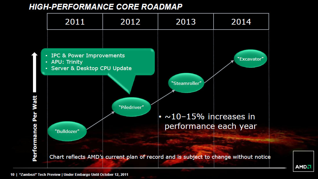