Home » servers (Page 2)
Category Archives: servers
AMD’s dense server strategy of mixing next-gen x86 Opterons with 64-bit ARM Cortex-A57 based Opterons on the SeaMicro Freedom™ fabric to disrupt the 2014 datacenter market using open source software (so far)
… so far, as Microsoft was in a “shut-up and ship” mode of operation during 2013 and could deliver its revolutionary Cloud OS with its even more disruptive Big Data solution for x86 only (that is likely to change as 64-bit ARM will be delivered with servers in H2 CY14).
Update: Disruptive Technologies for the Datacenter – Andrew Feldman, GM and CVP, AMD [Open Compute Project, Jan 28, 2014]


Note from the press release given below that: “The AMD Opteron A-Series development kit is packaged in a Micro-ATX form factor”. Take the note of the topmost message: “Optimized for dense compute – High-density, power-sensitive scale-out workloads: web hosting, data analytics, caching, storage”.


AMD to Accelerate the ARM Server Ecosystem with the First ARM-based CPU and Development Platform from a Server Processor Vendor [press release, Jan 28, 2014]
AMD also announced the imminent sampling of the ARM-based processor, named the AMD Opteron™ A1100 Series, and a development platform, which includes an evaluation board and a comprehensive software suite.

This should be the evaluation board for the development platform with imminent sampling.

In addition, AMD announced that it would be contributing to the Open Compute Project a new micro-server design using the AMD Opteron A-Series, as part of the common slot architecture specification for motherboards dubbed “Group Hug.”
| From OCP Summit IV: Breaking Up the Monolith [blog of the Open Compute Project, Jan 16, 2013] … “Group Hug” board: Facebook is contributing a new common slot architecture specification for motherboards. This specification — which we’ve nicknamed “Group Hug” — can be used to produce boards that are completely vendor-neutral and will last through multiple processor generations. The specification uses a simple PCIe x8 connector to link the SOCs to the board. … How does AMD support the Open Compute common slot architecture? [AMD YouTube channel, Oct 3, 2013] Learn more about AMD Open Compute: http://bit.ly/AMD_OpenCompute Dense computing is the latest trend in datacenter technology, and the Open Compute Project is driving standards codenamed Common Slot. In this video, AMD explains Common Slot and how the AMD APU and ARM offerings will power next generation data centers.
See also: Facebook Saved Over A Billion Dollars By Building Open Sourced Servers [TechCrunch, Jan 28, 2014] |


The AMD Opteron A-Series processor, codenamed “Seattle,” will sample this quarter along with a development platform that will make software design on the industry’s premier ARM–based server CPU quick and easy. AMD is collaborating with industry leaders to enable a robust 64-bit software ecosystem for ARM-based designs from compilers and simulators to hypervisors, operating systems and application software, in order to address key workloads in Web-tier and storage data center environments. The AMD Opteron A-Series development platform will be supported by a broad set of tools and software including a standard UEFI boot and Linux environment based on the Fedora Project, a Red Hat-sponsored, community-driven Linux distribution.
…AMD continues to drive the evolution of the open-source data center from vision to reality and bring choice among processor architectures. It is contributing the new AMD Open CS 1.0 Common Slot design based on the AMD Opteron A-Series processor compliant with the new Common Slot specification, also announced today, to the Open Compute Project.
…

AMD announces plans to sample 64-bit ARM Opteron A “Seattle” processors [AMD Blogs > AMD Business, Jan 28, 2014]
AMD’s rich history in server-class silicon includes a number of notable firsts including the first 64-bit x86 architecture and true multi-core x86 processors. AMD adds to that history by announcing that its revolutionary AMD Opteron™ A-series 64-bit ARM processors, codenamed “Seattle,” will be sampling this quarter.
AMD Opteron A-Series processors combine AMD’s expertise in delivering server-class silicon with ARM’s trademark low-power architecture and contributing to the Open Source software ecosystem that is rapidly growing around the ARM 64-bit architecture. AMD Opteron A-Series processors make use of ARM’s 64-bit ARMv8 architecture to provide true server-class features in a power efficient solution.
AMD plans for the AMD Opteron™ A1100 processors to be available in the second half of 2014 with four or eight ARM Cortex A57 cores, up to 4MB of shared Level 2 cache and 8MB of shared Level 3 cache. The AMD Opteron A-Series processor supports up to 128GB of DDR3 or DDR4 ECC memory as unbuffered DIMMs, registered DIMMs or SODIMMs.
The ARMv8 architecture is the first from ARM to have 64-bit support, something that AMD brought to the x86 market in 2003 with the AMD Opteron processor. Not only can the ARMv8-based Cortex A-57 architecture address large pools of memory, it has been designed from the ground up to provide the optimal balance of performance and power efficiency to address the broad spectrum of scale-out data center workloads.
With more than a decade of experience in designing server-class solutions silicon, AMD took the ARM Cortex A57 core, added a server-class memory controller, and included features resulting in a processor that meets the demands of scale-out workloads. A requirement of scale-out workloads is high performance connectivity, and the AMD Opteron A1100 processor has extensive integrated I/O, including eight PCI Express Gen 3 lanes, two 10 GB/s Ethernet and eight SATA 3 ports.
Scale-out workloads are becoming critical building blocks in today’s data centers. These workloads scale over hundreds or thousands of servers, making power efficient performance critical in keeping total cost of ownership (TCO) low. The AMD Opteron A-Series meets the demand of these workloads through intelligent silicon design and by supporting a number of operating system and software projects.
As part of delivering a server-class solution, AMD has invested in the software ecosystem that will support AMD Opteron A-Series processors. AMD is a gold member of the Linux Foundation, the organisation that oversees the development of the Linux kernel, and is a member of Linaro, a significant contributor to the Linux kernel. Alongside collaboration with the Linux Foundation and Linaro, AMD itself is listed as a top 20 contributor to the Linux kernel. A number of operating system vendors have stated they will support the 64-bit ARM ecosystem, including Canonical, Red Hat and SUSE, while virtualization will be enabled through KVM and Xen.
Operating system support is supplemented with programming language support, with Oracle and the community-driven OpenJDK porting versions of Java onto the 64-bit ARM architecture. Other popular languages that will run on AMD Opteron A-Series processors include Perl, PHP, Python and Ruby. The extremely popular GNU C compiler and the critical GNU C Library have already been ported to the 64-bit ARM architecture.
Through the combination of kernel support and development tools such as libraries, compilers and debuggers, the foundation has been set for developers to port applications to a rapidly growing ecosystem.
As AMD Opteron A-Series processors are well suited to web hosting and big data workloads, AMD is a gold sponsor of the Apache Foundation, the organisation that manages the Hadoop and HTTP Server projects. Up and down the software stack, the ecosystem is ready for the data center revolution that will take place when AMD Opteron A-Series are deployed.
Soon, AMD’s partners will start to realise what a true server-class 64-bit ARM processor can do. By using AMD’s Opteron A-Series Development Kit, developers can contribute to the fast growing software ecosystem that already includes operating systems, compilers, hypervisors and applications. Combining AMD’s rich history in designing server-class solutions with ARM’s legendary low-power architecture, the Opteron A-Series ushers in the era of personalised performance.
Introducing the industry’s only 64-bit ARM-based server SoC from AMD [AMD YouTube channel, Jan 21, 2014]
It Begins: AMD Announces Its First ARM Based Server SoC, 64-bit/8-core Opteron A1100 [AnandTech, Jan 28, 2014]
… AMD will be making a reference board available to interested parties starting in March, with server and OEM announcements to come in Q4 of this year.
It’s still too early to talk about performance or TDPs, but AMD did indicate better overall performance than its Opteron X2150 (4-core 1.9GHz Jaguar) at a comparable TDP:

AMD alluded to substantial cost savings over competing Intel solutions with support for similar memory capacities. AMD tells me we should expect a total “solution” price somewhere around 1/10th that of a competing high-end Xeon box, but it isn’t offering specifics beyond that just yet. Given the Opteron X2150 performance/TDP comparison, I’m guessing we’re looking at a similar ~$100 price point for the SoC. There’s also no word on whether or not the SoC will leverage any of AMD’s graphics IP. …
End of Update
AMD is also in a quite unique market position now as its only real competitor, Calxeda shut down its operation on December 19, 2013 and went into restructuring. The reason for that was lack of further funding by venture capitalists attributed mainly to its initial 32-bit Cortex-A15 based approach and the unwillingness of customers and software partners to port their already 64-bit x86 software back to 32-bit.
With the only remaining competitor in the 64-bit ARM server SoC race so far*, Applied Micro’s X-Gene SoC being built on a purpose built core of its own (see also my Software defined server without Microsoft: HP Moonshot [‘Experiencing the Cloud’, April 10, Dec 6, 2013] post), i.e. with only architecture license taken from ARM Holdings, the volume 64-bit ARM server SoC market starting in 2014 already belongs to AMD. I would base that prediction on the AppliedMicro’s X-Gene: 2013 Year in Review [Dec 20, 2013] post, stating that the first-generation X-Gene product is just nearing volume production, and a pilot X-Gene solution is planned only for early 2014 delivery by Dell.
* There is also Cavium which has too an ARMv8 architecture license only (obtained in August, 2012) but for this the latest information (as of Oct 30, 2013) was that: “In terms of the specific announcement of the product, we want to do it fairly close to silicon. We believe that this is a very differentiated product, and we would like to kind of keep it under the covers as long as we can. Obviously our customers have all the details of the products, and they’re working with them, but on a general basis for competitive reasons, we are kind of keeping this a little bit more quieter than we normally do.”
Meanwhile the 64-bit x86 based SeaMicro solution has been on the market since July 30, 2010, after 3 years in development. At the time of SeaMicro acquisition by AMD (Feb 29, 2012) this already represented a quite well thought-out and engineered solution, as one can easily grasp from the information included below:

1. IOVT: I/O-Virtualization Technology
2. TIO: Turn It Off

3. Freedom™ Supercomputer Fabric: 3D torus network fabric
– 8 x 8 x 8 Fabric nodes
– Diameter (max hop) 4 + 4 + 4 = 12
– Theor. cross section bandwidth = 2 (periodic) x 8 x 8 (section) x 2(bidir) x 2.0Gbs/link = 512Gb/s
– Compute, storage, mgmt cards are plugged into the network fabric
– Support for hot plugged compute cards
The first three—IOVT, TIO, and the Freedom™ Supercomputer Fabric—live in SeaMicro’s Freedom™ ASIC. Freedom™ ASICs are paired with each CPU and with DRAM, forming the foundational building block of a SeaMicro system.
4. DCAT: Dynamic Computation-Allocation Technology™
– CPU management and load balancing
– Dynamic workload allocation to specific CPUs on the basis of power-usage metrics
– Users can create pools of compute for a given application
– Compute resources can be dynamically added to the pool based on predefined utilization thresholds
The DCAT technology resides in the SeaMicro system software and custom-designed FPGAs/NPUs, which control and direct the I/O traffic.
More information:
– SeaMicro SM10000-64 Server [SeaMicro presentation on Hot Chips 23, Aug 19, 2011] for slides in PDF format while the presentation itself is the first one in the following recorded video (just the first 20 minutes + 7 minutes of—quite valuable—Q&A following that):
Session 7, Hot Chips 23 (2011), Friday, August 19, 2011. SeaMicro SM10000-64 Server: Building Data Center Servers Using “Cell Phone” Chips Ashutosh Dhodapkar, Gary Lauterbach, Sean Lie, Dhiraj Mallick, Jim Bauman, Sundar Kanthadai, Toru Kuzuhara, Gene Shen, Min Xu, and Chris Zhang, SeaMicro Poulson: An 8-Core, 32nm, Next-Generation Intel Itanium Processor Stephen Undy, Intel T4: A Highly Threaded Server-on-a-Chip with Native Support for Heterogenous Computing Robert Golla and Paul Jordan, Oracle
– SeaMicro Technology Overview [Anil Rao from SeaMicro, January 2012]
– System Overview for the SM10000 Family [Anil Rao from SeaMicro, January 2012]
Note that the above is just for the 1st generation as after the AMD acquisition (Feb 29, 2012) a second generation solution came out with the SM15000 enclosure (Sept 10, 2012 with more info in the details section later), and certainly there will be a 3d generation solution with the integrated into the each of x86 and 64-bit ARM based SoCs coming in 2014.
With the “only production ready, production tested supercompute fabric” (as was touted by Rory Read, CEO of AMD more than a year ago), the SeaMicro Freedom™ now will be integrated into the upcoming 64-bit ARM Cortex-A57 based “Seattle” chips from AMD, sampling in the first quarter of 2014. Consequently I would argue that even the high-end market will be captured by the company. Moreover, I think this will not be only in the SoC realm but in enclosures space as well (although that 3d type of enclosure is still to come), to detriment of HP’s highly marketed Moonshot and CloudSystem initiatives.
Then here are two recent quotes from the top executive duo of AMD showing the importance of their upcoming solution as they view it themselves:
Rory Read – AMD’s President and CEO [Oct 17, 2013]:
In the server market, the industry is at the initial stages of a multiyear transition that will fundamentally change the competitive dynamic. Cloud providers are placing a growing importance on how they get better performance from their datacenters while also reducing the physical footprint and power consumption of their server solution.

Lisa Su – AMD’s Senior Vice President and General Manager, Global Business Units [Oct 17, 2013]:
We are fully top to bottom in 28 nanometer now across all of our products, and we are transitioning to both 20 nanometer and to FinFETs over the next couple of quarters in terms of designs. … [Regarding] the SeaMicro business, we are very pleased with the pipeline that we have there. Verizon was the first major datacenter win that we can talk about publicly. We have been working that relationship for the last two years. …
… We’re very excited about the server space. It’s a very good market. It’s a market where there is a lot of innovation and change. In terms of 64-bit ARM, you will see us sampling that product in the first quarter of 2014. That development is on schedule and we’re excited about that. All of the customer discussions have been very positive and then we will combine both the [?x86 and the?]64-bit ARM chip with our SeaMicro servers that will have full solution as well. You will see SeaMicro plus ARM in 2014.
So I think we view this combination of IP as really beneficial to accelerating the dense server market both on the chip side and then also on the solution side with the customer set.
AMD SeaMicro has been extensively working with key platform software vendors, especially in the open source space:

The current state of that collaboration is reflected in the corresponding numbered sections coming after the detailed discussion (given below before the numbered sections):
- Verizon (as its first big name cloud customer, actually not using OpenStack)
- OpenStack (inc. Rackspace, excl. Red Hat)
- Red Hat
- Ubuntu
- Big Data, Hadoop
So let’s take a detailed look at the major topic:
AMD in the Demo Theater [OpenStack Foundation YouTube channel, May 8, 2013]
Note that the OpenStack Quantum networking project was renamed Neutron after April, 2013. Details on the OpenStack effort will be provided later in the post.
Rory Read – AMD President and CEO [Oct 30, 2012]:
That SeaMicro Freedom™ fabric is ultimately very-very important. It is the only production ready, production tested supercompute fabric on the planet.
Lisa Su – AMD Senior Vice President and General Manager, Global Business Units [Oct 30, 2012]:
The biggest change in the datacenter is that there is no one size fits all. So we will offer ARM-based CPUs with our fabric. We will offer x86-based CPUs with our fabric. And we will also look at opportunities where we can merge the CPU technology together with graphics compute in an APU form-factor that will be very-very good for specific workloads in servers as well. So AMD will be the only company that’s able to offer the full range of compute horsepower with the right workloads in the datacenter.
AMD makes ARM Cortex-A57 64bit Server Processor [Charbax YouTube channel, Oct 30, 2012]
From AMD Changes Compute Landscape as the First to Bridge Both x86 and ARM Processors for the Data Center [press release, Oct 29, 2012]
This strategic partnership with ARM represents the next phase of AMD’s strategy to drive ambidextrous solutions in emerging mega data center solutions. In March, AMD announced the acquisition of SeaMicro, the leader in high-density, energy-efficient servers. With this announcement, AMD will integrate the AMD SeaMicro Freedom fabric across its leadership AMD Opteron x86- and ARM technology-based processors that will enable hundreds, or even thousands of processor clusters to be linked together to provide the most energy-efficient solutions.
AMD ARM Oct 29, 2012 Full length presentation [Manny Janny YouTube channel, Oct 30, 2012]
Rory Read – AMD President and CEO: [3:27] That SeaMicro Freedom™ fabric is ultimately very-very important in this announcement. It is the only production ready, production tested supercompute fabric on the planet. [3:41]
Lisa Su – Senior Vice President and General Manager, Global Business Units: [13:09] The biggest change in the datacenter is that there is no one size fits all. So we will offer ARM-based CPUs with our fabric. We will offer x86-based CPUs with our fabric. And we will also look at opportunities where we can merge the CPU technology together with graphics compute in an APU form-factor that will be very-very good for specific workloads in servers as well. So AMD will be the only company that’s able to offer the full range of compute horsepower with the right workloads in the datacenter [13:41]
From AMD to Acquire SeaMicro: Accelerates Disruptive Server Strategy [press release, Feb 29, 2012]
AMD (NYSE: AMD) today announced it has signed a definitive agreement to acquire SeaMicro, a pioneer in energy-efficient, high-bandwidth microservers, for approximately $334 million, of which approximately $281 million will be paid in cash. Through the acquisition of SeaMicro, AMD will be accelerating its strategy to deliver disruptive server technology to its OEM customers serving cloud-centric data centers. With SeaMicro’s fabric technology and system-level design capabilities, AMD will be uniquely positioned to offer industry-leading server building blocks tuned for the fastest-growing workloads such as dynamic web content, social networking, search and video. …
… “Cloud computing has brought a sea change to the data center–dramatically altering the economics of compute by changing the workload and optimal characteristics of a server,” said Andrew Feldman, SeaMicro CEO, who will become general manager of AMD’s newly created Data Center Server Solutions business. “SeaMicro was founded to dramatically reduce the power consumed by servers, while increasing compute density and bandwidth. By becoming a part of AMD, we will have access to new markets, resources, technology, and scale that will provide us with the opportunity to work tightly with our OEM partners as we fundamentally change the server market.”
ARM TechCon 2012 SoC Partner Panel: Introducing the ARM Cortex-A50 Series [ARMflix YouTube channel, recorded on Oct 30, published on Nov 13, 2012]
** Note that nearly 14 months later, on Dec 19, 2013 Calxeda ran out of its ~$100M venture capital accumulated earlier. As the company was not able to secure further funding it shut down its operation by dismissing most of its employees (except 12 workers serving existing customers) and went into “restructuring” with just putting on their company website: “We will update you as we conclude our restructuring process”. This is despite of the kind of pioneering role the company had, especially with HP’s Moonshot and CloudSystem initiatives, and the relatively short term promise of delivering its server cartridge to HP’s next-gen Moonshot enclosure as was well reflected in my Software defined server without Microsoft: HP Moonshot [‘Experiencing the Cloud’, April 10, Dec 6, 2013] post. The major problem was that “it tried to get to market with 32-bit chip technology, at a time most x86 servers boast 64-bit technology … [and as] customers and software companies weren’t willing to port their software to run on 32-bit systems” – reported the Wall Street Journal. I would also say that AMD’s “only production ready, production tested supercompute fabric on the planet” (see AMD Rory’s statement already given above) with its upcoming “Seattle” 64-bit ARM SoC to be on track for delivery in H2 CY14 was another major reason for the lack of additional venture funds to Calxeda.
AMD’s 64-bit “Seattle” ARM processor brings best of breed hardware and software to the data center [AMD Business blog, Dec 12, 2013]
Going into 2014, the server market is set to face the biggest disruption since AMD launched the 64-bit x86 AMD Opteron™ processor – the first 64-bit x86 processor – in 2003. Processors based on ARM’s 64-bit ARMv8 architecture will start to appear next year, and just like the x86 AMD Opteron™ processors a decade ago, AMD’s ARM 64-bit processors will offer enterprises a viable option for efficiently handling vast amounts of data.

From: AMD Unveils Server Strategy and Roadmap [press release June 18, 2013]
Note that AMD Details Embedded Product Roadmap [press release, Sept, 9, 2013] as well in which there is also a:
|

The AMD Opteron processor came at a time when x86 processors were seen by many as silicon that could only power personal computers, with specialized processors running on architectures such as SPARC™ and Power™ being the ones that were handling server workloads. Back in 2003, the AMD Opteron processor did more than just offer another option, it made the x86 architecture a viable contender in the server market – showing that processors based on x86 architectures could compete effectively against established architectures. Thanks in no small part to the AMD Opteron processor, today the majority of servers shipped run x86 processors.
In 2014, AMD will once again disrupt the datacenter as x86 processors will be joined by those that make use of ARM’s 64-bit architecture. Codenamed “Seattle,” AMD’s first ARM-based Opteron processor will use the ARMv8 architecture, offering low-power processing in the fast growing dense server space.
To appreciate what the first ARM-based AMD Opteron processor is designed to deliver to those wanting to deploy racks of servers, it is important to realize that the ARMv8 architecture offers a clean slate on which to build both hardware and software.
ARM’s ARMv8 architecture is much more than a doubling of word-length from previous generation ARMv7 architecture: it has been designed from the ground-up to provide higher performance while retaining the trademark power efficiencies that everyone has come to expect from the ARM architecture. AMD’s “Seattle” processors will have either four or eight cores, packing server-grade features such as support for up to 128 GB of ECC memory, and integrated 10Gb/sec of Ethernet connectivity with AMD’s revolutionary Freedom™ fabric, designed to cater for dense compute systems.
|
From: AMD Delivers a New Generation of AMD Opteron and Intel Xeon “Ivy Bridge” Processors in its New SeaMicro SM15000 Micro Server Chassis [press release, Sept 10, 2012]
AMD off-chip interconnect fabric IP designed to enable significantly lower TCO • Links hundreds –> thousands of SoC modules • Shares hundreds of TBs storage and virtualizes I/O • 160Gbps Ethernet Uplink • Instruction Set:
Freedom™ ASIC 2.0 – Industry’s only Second Generation Fabric TechnologyThe Freedom™ ASIC is the building block of SeaMicro Fabric Compute Systems, enabling interconnection of energy efficient servers in a 3-dimensional Torus Fabric. The second generation Freedom ASIC includes high performance network interfaces, storage connectivity, and advanced server management, thereby eliminating the need for multiple sets of network adapters, HBAs, cables, and switches. This results in unmatched density, energy efficiency, and lowered TCO. Some of the key technologies in ASIC 2.0 include:
Unified Management – Easily Provision and Manage Servers, Network, and Storage Resources on DemandThe SeaMicro SM15000 implements a rich management system providing unified management of servers, network, and storage. Resources can be rapidly deployed, managed, and repurposed remotely, enabling lights-off data center operations. It offers a broad set of management API including an industry standard CLI, SNMP, IPMI, syslog, and XEN APIs, allowing customers to seamlessly integrate the SeaMicro SM15000 into existing data center management environments.Redundancy and Availability – Engineered from the Ground Up to Eliminate Single Points of FailureThe SeaMicro SM15000 is designed for the most demanding environments, helping to ensure availability of compute, network, storage, and system management. At the heart of the system is the Freedom Fabric, interconnecting all resources in the system, with the ability to sustain multiple points of failure and allow live component servicing. All active components in the system can be configured redundant and are hot-swappable, including server cards, network uplink cards, storage controller cards, system management cards, disks, fan trays, and power supplies. Key resources can also be configured to be protected in the following ways:Compute – A shared spare server can be configured to act as a standby spare for multiple primary servers. In the event of failure, the primary server’s personality, including MAC address, assigned disks, and boot configuration can be migrated to the standby spare and brought back online – ensuring fast restoration of services from a remote location.Network – The highly available fabric ensures network connectivity is maintained between servers and storage in the event of path failure. For uplink high-availability, the system can be configured with multiple uplink modules and port channels providing redundant active/active interfaces.Storage – The highly available fabric ensures that servers can access fabric storage in the event of failures. The fabric storage system also provides an efficient, high utilization optional hardware RAID to protect data in case of disk failure.
|


We realize that having an impressive set of hardware features in the first ARM-based Opteron processors is half of the story, and that is why we are hard at work on making sure the software ecosystem will support our cutting edge hardware. Work on software enablement has been happening throughout the stack – from the UEFI, to the operating system and onto application frameworks and developer tools such as compilers and debuggers. This ensures that the software will be ready for ARM-based servers.
|
AMD developing Linux on ARM at Linaro Connect 2013 [Charbax YouTube channel, March 11, 2013] [Recorded at Linaro Connect Asia 2013, March 4-8, 2013] Dr. Leendert van Doorn, Corporate Fellow at AMD, talks about what AMD does with Linaro to optimize Linux on ARM. He talks about the expectations that AMD has for results to come from Linaro in terms of achieving a better and more fully featured Linux world on ARM, especially for the ARM Cortex-A57 ARMv8 processor that AMD has announced for the server market.
|
AMD’s participation in software projects is well documented, being a gold member of the Linux Foundation, the organization that manages the development of the Linux kernel, and a group member of Linaro. AMD is a gold sponsor of the Apache Foundation, which oversees projects such as Hadoop, HTTP Server and Samba among many others, and the company’s engineers are contributors to the OpenJDK project. This is just a small selection of the work AMD is taking part in, and these projects in particular highlight how important AMD feels that open source software is to the data center, and in particular micro servers, that make use of ARM-based processors.
And running ARM-based processors doesn’t mean giving up on the flexibility of virtual machines, with KVM already ported to the ARMv8 architecture. Another popular hypervisor, Xen, is already available for 32-bit ARM architectures with a 64-bit port planned, ensuring that two popular and highly capable hypervisors will be available.
The Linux kernel has supported 64-bit ARMv8 architecture since Linux 3.7, and a number of popular Linux distributions have already signaled their support for the architecture including Canonical’s Ubuntu and the Red Hat sponsored Fedora distribution. In fact there is a downloadable, bootable Ubuntu distribution available in anticipation for ARMv8-based processors.
It’s not just operating systems and applications that are available. Developer tools such as the extremely popular open source GCC compiler and the vital GNU C Library (Glibc) have already been ported to the ARMv8 architecture and are available for download. With GCC and Glibc good to go, a solid foundation for developers to target the ARMv8 architecture is forming.
All of this work on both hardware and software should shed some light on just how big ARM processors will be in the data center. AMD, an established enterprise semiconductor vendor, is uniquely placed to ship both 64-bit ARMv8 and 64-bit x86 processors that enable “mixed rack” environments. And thanks to the army of software engineers at AMD, as well as others around the world who have committed significant time and effort, the software ecosystem will be there to support these revolutionary processors. 2014 is set to see the biggest disruption in the data center in over a decade, with AMD again at the center of it.
Lawrence Latif is a blogger and technical communications representative at AMD. His postings are his own opinions and may not represent AMD’s positions, strategies or opinions. Links to third party sites, and references to third party trademarks, are provided for convenience and illustrative purposes only. Unless explicitly stated, AMD is not responsible for the contents of such links, and no third party endorsement of AMD or any of its products is implied.
End of AMD’s 64-bit “Seattle” ARM processor brings best of breed hardware and software to the data center [AMD Business blog, Dec 12, 2013]
AMD at ARM Techcon 2013 [Charbax YouTube channel, recorded at the ARM Techcon 2013 (Oct 29-31), published on Dec 25, 2013]
From: Advanced Micro Devices’ CEO Discusses Q3 2013 Results – Earnings Call Transcript [Seeking Alpha, Oct 17, 2013]
Rory Read – President and CEO:
The three step turnaround plan we outlined a year ago to restructure, accelerate and ultimately transform AMD is clearly paying off. We completed the restructuring phase of our plan, maintaining cash at optimal levels and beating our $450 million quarterly operating expense goal in the third quarter. We are now in the second phase of our strategy – accelerating our performance by consistently executing our product roadmap while growing our new businesses to drive a return to profitability and positive free cash flow.
We are also laying the foundation for the third phase of our strategy, as we transform AMD to compete across a set of high growth markets. Our progress on this front was evident in the third quarter as we generated more than 30% of our revenue from our semi-custom and embedded businesses. Over the next two years we will continue to transform AMD to expand beyond a slowing, transitioning PC industry, as we create a more diverse company and look to generate approximately 50% of our revenue from these new high growth markets.
We have strategically targeted that semi-custom, ultra-low power client, embedded, dense server and the professional graphics market where we can offer differentiated products that leverage our APU and graphics IP. Our strategy allows us to continue to invest in the product that will drive growth, while effectively managing operating expenses. …
… Several of our growth businesses passed key milestones in the third quarter. Most significantly, our semi-custom business ramped in the quarter. We successfully shipped millions of units to support Sony and Microsoft, as they prepared to launch their next-generation game consoles. Our game console wins are generating a lot of customer interest, as we demonstrate our ability to design and reliably ramp production on two of the most complex SOCs ever built for high-volume consumer devices. We have several strong semi-custom design opportunities moving through the pipeline as customers look to tap into AMD’s IP, design and integration expertise to create differentiated winning solutions. … it’s our intention to win and mix in a whole set semicustom offerings as we build out this exciting and important new business.
We made good progress in our embedded business in the third quarter. We expanded our current embedded SOC offering and detailed our plans to be the only company to offer both 64-bit x86 and ARM solutions beginning in 2014. We have developed a strong embedded design pipeline which, we expect, will drive further growth for this business across 2014.
We also continue to make steady progress in another of our growth businesses in the third quarter, as we delivered our fifth consecutive quarter of revenue and share growth in the professional graphics area. We believe we can continue to gain share in this lucrative part of the GPU market, based on our product portfolio, design wins [in place] [ph] and enhanced channel programs.
In the server market, the industry is at the initial stages of a multiyear transition that will fundamentally change the competitive dynamic. Cloud providers are placing a growing importance on how they get better performance from their datacenters while also reducing the physical footprint and power consumption of their server solution.
This will become the defining metric of this industry and will be a key growth driver for the market and the new AMD. AMD is leading this emerging trend in the server market and we are committed to defining a leadership position.
Earlier this quarter, we had a significant public endorsement of our dense server strategy as Verizon announced a high performance public cloud that uses our SeaMicro technology and Opteron processor. We remain on track to introduce new, low-power X86 and 64-bit ARM processors next year and we believe we will offer the industry leading ARM-based servers. …
… Two years ago we were 90% to 95% of our business centered over PCs and we’ve launched the clear strategy to diversify our portfolio taking our IT — leadership IT and Graphics and CPU and taking it into adjacent segment where there is high growth for three, five, seven years and stickier opportunities.
We see that as an opportunity to drive 50% or more of our business over that time horizon. And if you look at the results in the third quarter, we are already seeing the benefits of that opportunity with over 30% of our revenue now coming from semi-custom and our embedded businesses.
We see it is an important business in PC, but its time is changing and the go-go era is over. We need to move and attack the new opportunities where the market is going, and that’s what we are doing.
Lisa Su – Senior Vice President and General Manager, Global Business Units:
We are fully top to bottom in 28 nanometer now across all of our products, and we are transitioning to both 20 nanometer and to FinFETs over the next couple of quarters in terms of designs. We will do 20 nanometer first, and then we will go to FinFETs. …
… game console semicustom product is a long life cycle product over five to seven years. Certainly when we look at cost reduction opportunities, one of the important ones is to move technology nodes. So we will in this timeframe certainly move from 28 nanometer to 20 nanometer and now the reason to do that is both for pure die cost savings as well as all the power savings that our customer benefits from. … so expect the cost to go down on a unit basis as we move to 20.
[Regarding] the SeaMicro business, we are very pleased with the pipeline that we have there. Verizon was the first major datacenter win that we can talk about publicly. We have been working that relationship for the last two years. So it’s actually nice to be able to talk about it. We do see it as a major opportunity that will give us revenue potential in 2014. And we continue to see a strong pipeline of opportunities with SeaMicro as more of the datacenter guys are looking at how to incorporate these dense servers into their new cloud infrastructures. …
… As I said the Verizon engagement has lasted over the past two years. So some of the initial deployments were with the Intel processors but we do have significant deployments with AMD Opteron as well. We do see the percentage of Opteron processors increasing because that’s what we’d like to do. …
We’re very excited about the server space. It’s a very good market. It’s a market where there is a lot of innovation and change. In terms of 64-bit ARM, you will see us sampling that product in the first quarter of 2014. That development is on schedule and we’re excited about that. All of the customer discussions have been very positive and then we will combine both the [?x86 and the?]64-bit ARM chip with our SeaMicro servers that will have full solution as well. You will see SeaMicro plus ARM in 2014.
So I think we view this combination of IP as really beneficial to accelerating the dense server market both on the chip side and then also on the solution side with the customer set.
Amazon’s James Hamilton: Why Innovation Wins [AMD SeaMicro YouTube channel, Nov 12, 2012] video which was included into the Headline News and Events section of Volume 1, December 2012 of The Wave Newsletter from AMD SeaMicro with the following intro:
James Hamilton, VP and Distinguished Engineer at Amazon called AMD’s co-announcement with ARM to develop 64-bit ARM technology-based processors “A great day for the server ecosystem.” Learn why and hear what James had to say about what this means for customers and the broader server industry.
AMD Changes Compute Landscape as the First to Bridge Both x86 and ARM Processors for the Data Center [press release, Oct 29, 2012]
Company to Complement x86-based Offerings with New Processors Based on ARM 64-bit Technology, Starting with Server Market
SUNNYVALE, Calif. —10/29/2012
In a bold strategic move, AMD (NYSE: AMD) announced that it will design 64-bit ARM® technology-based processors in addition to its x86 processors for multiple markets, starting with cloud and data center servers. AMD’s first ARM technology-based processor will be a highly-integrated, 64-bit multicore System-on-a-Chip (SoC) optimized for the dense, energy-efficient servers that now dominate the largest data centers and power the modern computing experience. The first ARM technology-based AMD Opteron™ processor is targeted for production in 2014 and will integrate the AMD SeaMicro Freedom™ supercompute fabric, the industry’s premier high-performance fabric.
AMD’s new design initiative addresses the growing demand to deliver better performance-per-watt for dense cloud computing solutions. Just as AMD introduced the industry’s first mainstream 64-bit x86 server solution with the AMD Opteron processor in 2003, AMD will be the only processor provider bridging the x86 and 64-bit ARM ecosystems to enable new levels of flexibility and drive optimal performance and power-efficiency for a range of enterprise workloads.
“AMD led the data center transition to mainstream 64-bit computing with AMD64, and with our ambidextrous strategy we will again lead the next major industry inflection point by driving the widespread adoption of energy-efficient 64-bit server processors based on both the x86 and ARM architectures,” said Rory Read, president and chief executive officer, AMD. “Through our collaboration with ARM, we are building on AMD’s rich IP portfolio, including our deep 64-bit processor knowledge and industry-leading AMD SeaMicro Freedom supercompute fabric, to offer the most flexible and complete processing solutions for the modern data center.”
“The industry needs to continuously innovate across markets to meet customers’ ever-increasing demands, and ARM and our partners are enabling increasingly energy-efficient computing solutions to address these needs,” said Warren East, chief executive officer, ARM. “By collaborating with ARM, AMD is able to leverage its extraordinary portfolio of IP, including its AMD Freedom supercompute fabric, with ARM 64-bit processor cores to build solutions that deliver on this demand and transform the industry.”
The explosion of the data center has brought with it an opportunity to optimize compute with vastly different solutions. AMD is providing a compute ecosystem filled with choice, offering solutions based on AMD Opteron x86 CPUs, new server-class Accelerated Processing Units (APUs) that leverage Heterogeneous Systems Architecture (HSA), and new 64-bit ARM-based solutions.
This strategic partnership with ARM represents the next phase of AMD’s strategy to drive ambidextrous solutions in emerging mega data center solutions. In March, AMD announced the acquisition of SeaMicro, the leader in high-density, energy-efficient servers. With this announcement, AMD will integrate the AMD SeaMicro Freedom fabric across its leadership AMD Opteron x86- and ARM technology-based processors that will enable hundreds, or even thousands of processor clusters to be linked together to provide the most energy-efficient solutions.
“Over the past decade the computer industry has coalesced around two high-volume processor architectures – x86 for personal computers and servers, and ARM for mobile devices,” observed Nathan Brookwood, research fellow at Insight 64. “Over the next decade, the purveyors of these established architectures will each seek to extend their presence into market segments dominated by the other. The path on which AMD has now embarked will allow it to offer products based on both x86 and ARM architectures, a capability no other semiconductor manufacturer can likely match.”
At an event hosted by AMD in San Francisco, representatives from Amazon, Dell, Facebook and Red Hat participated in a panel discussion on opportunities created by ARM server solutions from AMD. A replay of the event can be found here as of 5 p.m. PDT, Oct. 29.
Supporting Resources
- AMD bridges the x86 and ARM ecosystems for the data center announcement press resources
- Follow AMD on Twitter at @AMD
- Follow the AMD and ARM announcement on Twitter at #AMDARM
- Like AMD on Facebook.
AMD SeaMicro SM15000 with Freedom Fabric Storage [AMD YouTube channel, Sept 11, 2012]
AMD Extends Leadership in Data Center Innovation – First to Optimize the Micro Server for Big Data [press release, Sept 10, 2012]
AMD’s SeaMicro SM15000™ Server Delivers Hyper-efficient Compute for Big Data and Cloud Supporting Five Petabytes of Storage; Available with AMD Opteron™ and Intel® Xeon® “Ivy Bridge”/”Sandy Bridge” Processors
SUNNYVALE, Calif. —9/10/2012
AMD (NYSE: AMD) today announced the SeaMicro SM15000™ server, another computing innovation from its Data Center Server Solutions (DCSS) group that cements its position as the technology leader in the micro server category. AMD’s SeaMicro SM15000 server revolutionizes computing with the invention of Freedom™ Fabric Storage, which extends its Freedom™ Fabric beyond the SeaMicro chassis to connect directly to massive disk arrays, enabling a single ten rack unit system to support more than five petabytes of low-cost, easy-to-install storage. The SM15000 server combines industry-leading density, power efficiency and bandwidth with a new generation of storage technology, enabling a single rack to contain thousands of cores, and petabytes of storage – ideal for big data applications like Apache™ Hadoop™ and Cassandra™ for public and private cloud deployments.
AMD’s SeaMicro SM15000 system is available today and currently supports the Intel® Xeon® Processor E3-1260L (“Sandy Bridge”). In November, it will support the next generation of AMD Opteron™ processors featuring the “Piledriver” core, as well as the newly announced Intel Xeon Processor E3-1265Lv2 (“Ivy Bridge”). In addition to these latest offerings, the AMD SeaMicro fabric technology continues to deliver a key building block for AMD’s server partners to build extremely energy efficient micro servers for their customers.
“Historically, server architecture has focused on the processor, while storage and networking were afterthoughts. But increasingly, cloud and big data customers have sought a solution in which storage, networking and compute are in balance and are shared. In a legacy server, storage is a captive resource for an individual processor, limiting the ability of disks to be shared across multiple processors, causing massive data replication and necessitating the purchase of expensive storage area networking or network attached storage equipment,” said Andrew Feldman, corporate vice president and general manager of the Data Center Server Solutions group at AMD. “AMD’s SeaMicro SM15000 server enables companies, for the first time, to share massive amounts of storage across hundreds of efficient computing nodes in an exceptionally dense form factor. We believe that this will transform the data center compute and storage landscape.”
AMD’s SeaMicro products transformed the data center with the first micro server to combine compute, storage and fabric-based networking in a single chassis. Micro servers deliver massive efficiencies in power, space and bandwidth, and AMD set the bar with its SeaMicro product that uses one-quarter the power, takes one-sixth the space and delivers 16 times the bandwidth of the best-in-class alternatives. With the SeaMicro SM15000 server, the innovative trajectory broadens the benefits of the micro server to storage, solving the most pressing needs of the data center.
Combining the Freedom™ Supercompute Fabric technology with the pioneering Freedom™ Fabric Storage technology enables data centers to provide more than five petabytes of storage with 64 servers in a single ten rack unit (17.5 inch tall) SM15000 system. Once these disks are interconnected with the fabric, they are seen and shared by all servers in the system. This approach provides the benefits typically provided by expensive and complex solutions such as network-attached storage and storage area networking with the simplicity and low cost of direct attached storage
“AMD’s SeaMicro technology is leading innovation in micro servers and data center compute,” said Zeus Kerravala, founder and principal analyst of ZK Research. “The team invented the micro server category, was the first to bring small-core servers and large-core servers to market in the same system, the first to market with a second-generation fabric, and the first to build a fabric that supports multiple processors and instruction sets. It is not surprising that they have extended the technology to storage. The bringing together of compute and petabytes of storage demonstrates the flexibility of the Freedom Fabric. They are blurring the boundaries of compute, storage and networking, and they have once again challenged the industry with bold innovation.”
Leaders Across the Big Data Community Agree
Dr. Amr Awadallah, CTO and Founder at Cloudera, the category leader that is setting the standard for Hadoop in the enterprise, observes: “The big data community is hungry for innovations that simplify the infrastructure for big data analysis while reducing hardware costs. As we hear from our vast big data partner ecosystem and from customers using CDH and
Cloudera Enterprise, companies that are seeking to gain insights across all their data want their hardware vendors to provide low cost, high density, standards-based compute that connects to massive arrays of low cost storage. AMD’s SeaMicro delivers on this promise.”
Eric Baldeschwieler, co-founder and CTO of Hortonworks and a pioneer in Hadoop technology, notes: “Petabytes of low cost storage, hyper-dense energy-efficient compute, connected with a supercompute-style fabric is an architecture particularly well suited for big data analytics and Hortonworks Data Platform. At Hortonworks, we seek to make Apache Hadoop easier to use, consume and deploy, which is in line with AMD’s goal to revolutionize and commoditize the storage and processing of big data. We are pleased to see leaders in the hardware community inventing technology that extends the reach of big data analysis.”
Matt Pfeil, co-founder and VP of customer solutions at DataStax, the leader in real-time mission-critical big data platforms, agrees: “At DataStax, we believe that extraordinary databases, such as Cassandra, running mission-critical applications, can be used by nearly every enterprise. To see AMD’s DCSS group bringing together efficient compute and petabytes of storage over a unified fabric in a single low-cost, energy-efficient solution is enormously exciting. The combination of the SM15000 server and best-in-class database, Cassandra, offer a powerful threat to the incumbent makers of both databases and the expensive hardware on which they reside.”
AMD’s SeaMicro SM15000™ Technology
AMD’s SeaMicro SM15000 server is built around the industry’s first and only second-generation fabric, the Freedom Fabric. It is the only fabric technology designed and optimized to work with Central Processor Units (CPUs) that have both large and small cores, as well as x86 and non-x86 CPUs. Freedom Fabric contains innovative technology including:
SeaMicro IOVT (Input/Output Virtualization Technology), which eliminates all but three components from the SeaMicro motherboard – CPU, DRAM, and the ASIC itself – thereby shrinking the motherboard, while reducing power, cost and space;
SeaMicro TIO™ (Turn It Off) technology, which enables further power optimization on the mini motherboard by turning off unneeded CPU and chipset functions. Together, SeaMicro IOVT and TIO technology produce the smallest and most power efficient motherboards available;
Freedom Supercompute Fabric creates a 1.28 terabits-per-second fabric that ties together 64 of the power-optimized mini-motherboards at low latency and low power with massive bandwidth;
SeaMicro Freedom Fabric Storage, which allows the Freedom Supercompute Fabric to extend out of the chassis and across the data center, linking not just components inside the chassis, but those outside as well.
AMD’s SeaMicro SM15000 Server Details
AMD’s SeaMicro SM15000 server will be available with 64 compute cards, each holding a new custom-designed single-socket octal core 2.0/2.3/2.8 GHz AMD Opteron processor based on the “Piledriver” core, for a total of 512 heavy-weight cores per system or 2,048 cores per rack. Each AMD Opteron processor can support 64 gigabytes of DRAM, enabling a single system to handle more than four terabytes of DRAM and over 16 terabytes of DRAM per rack. AMD’s SeaMicro SM15000 system will also be available with a quad core 2.5 GHz Intel Xeon Processor E3-1265Lv2 (“Ivy Bridge”) for 256 2.5 GHz cores in a ten rack unit system or 1,024 cores in a standard rack. Each processor supports up to 32 gigabytes of memory so a single SeaMicro SM15000 system can deliver up to two terabytes of DRAM and up to eight terabytes of DRAM per rack.
AMD’s SeaMicro SM15000 server also contains 16 fabric extender slots, each of which can connect to three different Freedom Fabric Storage arrays with different capacities:
FS 5084-L is an ultra-dense capacity-optimized storage system. It supports up to 84 SAS/SATA 3.5 inch or 2.5 inch drives in 5 rack units for up to 336 terabytes of capacity per-array and over five petabytes per SeaMicro SM15000 system;
FS 2012-L is a capacity-optimized storage system. It supports up to 12 3.5 inch or 2.5 inch drives in 2 rack units for up to 48 terabytes of capacity per-array or up to 768 terabytes of capacity per SeaMicro SM15000 system;
FS 2024-S is a performance-optimized storage system. It supports up to 24 2.5 inch drives in 2 rack units for up to 24 terabytes of capacity per-array or up to 384 terabytes of capacity per SM15000 system.
In summary, AMD’s SeaMicro SM15000 system:
- Stands ten rack units or 17.5 inches tall;
- Contains 64 slots for compute cards for AMD Opteron or Intel Xeon processors;
- Provides up to ten gigabits per-second of bandwidth to each CPU;
- Connects up to 1,408 solid state or hard drives with Freedom Fabric Storage
- Delivers up to 16 10 GbE uplinks or up to 64 1GbE uplinks;
- Runs standard off-the-shelf operating systems including Windows®, Linux, Red Hat and VMware and Citrix XenServer hypervisors.
Availability
AMD’s SeaMicro SM15000 server with Intel’s Xeon Processor E3-1260L “Sandy Bridge” is now generally available in the U.S and in select international regions. Configurations based on AMD Opteron processors and Intel Xeon Processor E3-1265Lv2 with the “Ivy Bridge” microarchitecture will be available in November, 2012. More information on AMD’s revolutionary SeaMicro family of servers can be found at www.seamicro.com/products.
1. Verizon
Verizon Cloud on AMD’s SeaMicro SM15000 [AMD YouTube channel, Oct 7, 2013]
Verizon Cloud Compute and Verizon Cloud Storage [The Wave Newsletter from AMD, December 2013]
With enterprise adoption of public cloud services at 10 percent1, Verizon identified a need for a cloud service that was secure, reliable and highly flexible with enterprise-grade performance guarantees. Large, global enterprises want to take advantage of the agility, flexibility and compelling economics of the public cloud, but the performance and reliability are not up to par for their needs. To fulfill this need, Verizon spent over two years identifying and developing software using AMD’s SeaMicro SM15000, the industry’s first and only programmable server hardware. The new services redefine the benchmarks for public cloud computing and storage performance and security.
Designed specifically for enterprise customers, the new services allow companies to use the same policies and procedures across the enterprise network and the public cloud. The close collaboration has resulted in cloud computing services with unheralded performance level guarantees that are offered with competitive pricing. The new cloud services are backed by the power of Verizon, including global data centers, global IP network and enterprise-grade managed security services. The performance and security innovations are expected to accelerate public cloud adoption by the enterprise for their mission critical applications. more >
Verizon Selects AMD’s SeaMicro SM15000 for Enterprise Class Services: Verizon Cloud Compute and Verizon Cloud Storage [AMD-Seamicro press release, Oct 7, 2013]
Verizon and AMD create technology that transforms the public cloud, delivering the industry’s most advanced cloud capabilities
SUNNYVALE, Calif. —10/7/2013
AMD (NYSE: AMD) today announced that Verizon is deploying SeaMicro SM15000™ servers for its new global cloud platform and cloud-based object storage service, whose public beta was recently announced. AMD’s SeaMicro SM15000 server links hundreds of cores together in a single system using a fraction of the power and space of traditional servers. To enable Verizon’s next generation solution, technology has been taken one step further: Verizon and AMD co-developed additional hardware and software technology on the SM15000 server that provides unprecedented performance and best-in-class reliability backed by enterprise-level service level agreements (SLAs). The combination of these technologies co-developed by AMD and Verizon ushers in a new era of enterprise-class cloud services by enabling a higher level of control over security and performance SLAs. With this technology underpinning the new Verizon Cloud Compute and Verizon Cloud Storage, enterprise customers can for the first time confidently deploy mission-critical systems in the public cloud.
“We reinvented the public cloud from the ground up to specifically address the needs of our enterprise clients,” said John Considine, chief technology officer at Verizon Terremark. “We wanted to give them back control of their infrastructure – providing the speed and flexibility of a generic public cloud with the performance and security they expect from an enterprise-grade cloud. Our collaboration with AMD enabled us to develop revolutionary technology, and it represents the backbone of our future plans.”
As part of its joint development, AMD and Verizon co-developed hardware and software to reserve, allocate and guarantee application SLAs. AMD’s SeaMicro Freedom™ fabric-based SM15000 server delivers the industry’s first and only programmable server hardware that includes a high bandwidth, low latency programmable interconnect fabric, and programmable data and control plane for both network and storage traffic. Leveraging AMD’s programmable server hardware, Verizon developed unique software to guarantee and deliver reliability, unheralded performance guarantees and SLAs for enterprise cloud computing services.
“Verizon has a clear vision for the future of the public cloud services—services that are more flexible, more reliable and guaranteed,” said Andrew Feldman, corporate vice president and general manager, Server, AMD. “The technology we developed turns the cloud paradigm upside down by creating a service that an enterprise can configure and control as if the equipment were in its own data center. With this innovation in cloud services, I expect enterprises to migrate their core IT services and mission critical applications to Verizon’s cloud services.”
“The rapid, reliable and scalable delivery of cloud compute and storage services is the key to competing successfully in any cloud market from infrastructure, to platform, to application; and enterprises are constantly asking for more as they alter their business models to thrive in a mobile and analytic world,” said Richard Villars, vice president, Datacenter & Cloud at IDC. “Next generation integrated IT solutions like AMD’s SeaMicro SM15000 provide a flexible yet high-performance platform upon which companies like Verizon can use to build the next generation of cloud service offerings.”
Innovative Verizon Cloud Capabilities on AMD’s SeaMicro SM15000 Server Industry Firsts
Verizon leveraged the SeaMicro SM15000 server’s ability to disaggregate server resources to create a cloud optimized for computing and storage services. Verizon and AMD’s SeaMicro engineers worked for over two years to create a revolutionary public cloud platform with enterprise class capabilities.
These new capabilities include:
- Virtual machine server provisioning in seconds, a fraction of the time of a legacy public cloud;
- Fine-grained server configuration options that match real life requirements, not just small, medium, large sizing, including processor speed (500 MHz to 2,000 MHz) and DRAM (.5 GB increments) options;
- Shared disks across multiple server instances versus requiring each virtual machine to have its own dedicated drive;
- Defined storage quality of service by specifying performance up to 5,000 IOPS to meet the demands of the application being deployed, compared to best-effort performance;
- Consistent network security policies and procedures across the enterprise network and the public cloud;
- Strict traffic isolation, data encryption, and data inspection with full featured firewalls that achieve Department of Defense and PCI compliance levels;
- Guaranteed network performance for every virtual machine with reserved network performance up to 500 Mbps compared to no guarantees in many other public clouds.
The public beta for Verizon Cloud will launch in the fourth quarter. Companies interested in becoming a beta customer can sign up through the Verizon Enterprise Solutions website: www.verizonenterprise.com/verizoncloud.
AMD’s SeaMicro SM15000 Server
AMD’s SeaMicro SM15000 system is the highest-density, most energy-efficient server in the market. In 10 rack units, it links 512 compute cores, 160 gigabits of I/O networking, more than five petabytes of storage with a 1.28 terabyte high-performance supercompute fabric, called Freedom™ Fabric. The SM15000 server eliminates top-of-rack switches, terminal servers, hundreds of cables and thousands of unnecessary components for a more efficient and simple operational environment.
AMD’s SeaMicro server product family currently supports the next generation AMD Opteron™ (“Piledriver”) processor, Intel® Xeon® E3-1260L (“Sandy Bridge”) and E3-1265Lv2 (“Ivy Bridge”) and Intel® Atom™ N570 processors. The SeaMicro SM15000 server also supports the Freedom Fabric Storage products, enabling a single system to connect with more than five petabytes of storage capacity in two racks. This approach delivers the benefits of expensive and complex solutions such as network attached storage (NAS) and storage area networking (SAN) with the simplicity and low cost of direct attached storage.
For more information on the Verizon Cloud implementation, please visit: www.seamicro.com/vzcloud.
About AMD
AMD (NYSE: AMD) designs and integrates technology that powers millions of intelligent devices, including personal computers, tablets, game consoles and cloud servers that define the new era of surround computing. AMD solutions enable people everywhere to realize the full potential of their favorite devices and applications to push the boundaries of what is possible. For more information, visit www.amd.com.
correction…Verizon is not using OpenStack, but they are using our hardware.
@cloud_attitude
2. OpenStack
OpenStack 101 – What Is OpenStack? [Rackspace YouTube channel, Jan 14, 2013]
OpenStack: The Open Source Cloud Operating System
- OpenStack Shared Services (identity, image, telemetry, orchestration): code-named Keystone (OpenStack Identity), code-named Glance (OpenStack Image Service), code-named Ceilometer (OpenStack Metering), code-named Heat (OpenStack Orchestration)
- Compute: code-named Nova
- Networking: the original Quantum naming had to be phased out in April, 2013 and in June, 2013 was replaced by Neutron
- Storage: code-named Cinder (OpenStack Block Storage), code-named Swift (OpenStack Object Storage)
- Projects incubated in the upcoming Icehouse release started on Nov 7, 2013 and planned for release on April 17, 2014:
- Database Service (Trove) – https://wiki.openstack.org/wiki/Trove
- Bare Metal (Ironic) – https://wiki.openstack.org/wiki/Ironic
- Queue Service (Marconi) – https://wiki.openstack.org/wiki/Marconi
- Data Processing (Savannah) – https://wiki.openstack.org/wiki/Savanna
Why OpenStack? [The Wave Newsletter from AMD, December 2013]
OpenStack continues to gain momentum in the market as more and more, larger, established technology and service companies move from evaluation to deployment. But why has OpenStack become so popular? In this issue, we discuss the business drivers behind the widespread adoption and why AMD’s SeaMicro SM15000 server is the industry’s best choice for a successful OpenStack deployment. If you’re considering OpenStack, learn about the options and hear winning strategies from experts featured in our most recent OpenStack webcasts. And in case you missed it, read about AMD’s exciting collaboration with Verizon enabling them to offer enterprise-caliber cloud services. more >
OpenStack the SeaMicro SM15000 – From Zero to 2,048 Cores in Less than One Hour [The Wave Newsletter from AMD, March 2013]
The SeaMicro SM15000 is optimized for OpenStack, a solution that is being adopted by both public and private cloud operators. Red 5 Studios recently deployed OpenStack on a 48 foot bus to power their new massive multiplayer online game Firefall. The SM15000 uniquely excels for object storage, providing more than 5 petabytes of direct attached storage in two data center racks. more >
State of the Stack [OpenStack Foundation YouTube channel, recorded on Nov 8 under official title “Stack Debate: Understanding OpenStack’s Future”, published on Nov 9, 2013]
The biggest issue with OpenStack project which “started without a benevolent dictator and/or architect” was mentioned there (watch from [6:40]) as a kind of: “The worst architectural decision you can make is stay with default networking for a production system because the default networking model in OpenStack is broken for use at scale”.
Then Randy Bias summarized that particular issue later in Neutron in Production: Work in Progress or Ready for Prime Time? [Cloudscaling blog, Dec 6, 2013] as:
Ultimately, it’s unclear whether all networking functions ever will be modeled behind the Neutron API with a bunch of plug-ins. That’s part of the ongoing dialogue we’re having in the community about what makes the most sense for the project’s future.
The bottom-line consensus was is that Neutron is a work in progress. Vanilla Neutron is not ready for production, so you should get a vendor if you need to move into production soon.
AMD’s SeaMicro SM15000 Is the First Server to Provide Bare Metal Provisioning to Scale Massive OpenStack Compute Deployments [press release, Nov 5, 2013]
Provides Foundation to Leverage OpenStack Compute for Large Networks of Virtualized and Bare Metal Servers
SUNNYVALE, Calif. and Hong Kong, OpenStack Summit —11/5/2013
AMD (NYSE: AMD) today announced that the SeaMicro SM15000™ server supports bare metal features in OpenStack® Compute. AMD’s SeaMicro SM15000 server is ideally suited for massive OpenStack deployments by integrating compute, storage and networking into a 10 rack unit system. The system is built around the Freedom™ fabric, the industry’s premier supercomputing fabric for scale out data center applications. The Freedom fabric disaggregates compute, storage and network I/O to provide the most flexible, scalable and resilient data center infrastructure in the industry. This allows customers to match the compute performance, storage capacity and networking I/O to their application needs. The result is an adaptive data center where any server can be mapped to any hard disk/SSD or network I/O to expand capacity or recover from a component failure.
“OpenStack Compute’s bare metal capabilities provide the scalability and flexibility to build and manage large-scale public and private clouds with virtualized and dedicated servers,” said Dhiraj Mallick, corporate vice president and general manager, Data Center Server Solutions, at AMD. “The SeaMicro SM15000 server’s bare metal provisioning capabilities should simplify enterprise adoption of OpenStack and accelerate mass deployments since not all work loads are optimized for virtualized environments.”
Bare metal computing provides more predictable performance than a shared server environment using virtual servers. In a bare metal environment there are no delays caused by different virtual machines contending for shared resources, since the entire server’s resources are dedicated to a single user instance. In addition, in a bare metal environment the performance penalty imposed by the hypervisor is eliminated, allowing the application software to make full use of the processor’s capabilities
In addition to leading in bare metal provisioning, AMD’s SeaMicro SM15000 server provides the ability to boot and install a base server image from a central server for massive OpenStack deployments. A cloud image containing the KVM, the OpenStack Compute image and other applications can be configured by the central server. The coordination and scheduling of this workflow can be managed by Heat, the orchestration application that manages the entire lifecycle of an OpenStack cloud for bare metal and virtual machines.
Supporting Resources
- Visit the AMD SeaMicro site
- Follow AMD on Twitter @seamicroinc
Scalable Fabric-based Object Storage with the SM15000 [The Wave Newsletter from AMD, March 2013]
The SeaMicro SM15000 is changing the economics of deploying object storage, delivering the storage of unprecedented amounts of data while using 1/2 the power and 1/3 the space of traditional servers. more >
SwiftStack with OpenStack Swift Overview [SwiftStack YouTube channel, Oct 4, 2012]
AMD’s SeaMicro SM15000 Server Achieves Certification for Rackspace Private Cloud, Validated for OpenStack [press release, Jan 30, 2013]
Providing unprecedented computing efficiency for “Nova in a Box” and object storage capacity for “Swift in a Rack”
3. Red Hat
OpenStack + SM15000 Server = 1,000 Virtual Machines for Red Hat [The Wave Newsletter from AMD, June 2013]
Red Hat deploys one SM15000 server to quickly and cost effectively build out a high capacity server cluster to meet the growing demands for OpenShift demonstrations and to accelerate sales. Red Hat OpenShift, which runs on Red Hat OpenStack, is Red Hat’s cloud computing Platform-as-a-Service (PaaS) offering. The service provides built-in support for nearly every open source programming language, including Node.js, Ruby, Python, PHP, Perl, and Java. OpenShift can also be expanded with customizable modules that allow developers to add other languages.
more >
Red Hat Enterprise Linux OpenStack Platform: Community-invented, Red Hat-hardened [RedHatCloud YouTube channel, Aug 5, 2013]
AMD’s SeaMicro SM15000 Server Achieves Certification for Red Hat OpenStack [press release, June 12, 2013]
BOSTON – Red Hat Summit —6/12/2013
AMD (NYSE: AMD) today announced that its SeaMicro SM15000™ server is certified for Red Hat® OpenStack, and that the company has joined the Red Hat OpenStack Cloud Infrastructure Partner Network. The certification ensures that the SeaMicro SM15000 server provides a rigorously tested platform for organizations building private or public cloud Infrastructure as a Service (IaaS), based on the security, stability and support available with Red Hat OpenStack. AMD’s SeaMicro solutions for OpenStack include “Nova in a Box” and “Swift in a Rack” reference architectures that have been validated to ensure consistent performance, supportability and compatibility.
The SeaMicro SM15000 server integrates compute, storage and networking into a compact, 10 RU (17.5 inches) form factor with 1.28 Tbps supercompute fabric. The technology enables users to install and configure thousands of computing cores more efficiently than any other server. Complex time-consuming tasks are completed within minutes due to the integration of compute, storage and networking. Operational fire drills, such as setting up servers on short notice, manually configuring hundreds of machines and re-provisioning the network to optimize traffic are all handled through a single, easy-to-use management interface.
“AMD has shown leadership in providing a uniquely differentiated server for OpenStack deployments, and we are excited to have them as a seminal member of the Red Hat OpenStack Cloud Infrastructure Partner Network,” said Mike Werner, senior director, ISV and Developer Ecosystems at Red Hat. “The SeaMicro server is an example of incredible innovation, and I am pleased that our customers will have the SM15000 system as an option for energy-efficient, dense computing as part of the Red Hat Certified Solution Marketplace.”
AMD’s SeaMicro SM15000 system is the highest-density, most energy-efficient server in the market. In 10 rack units, it links 512 compute cores, 160 gigabits of I/O networking and more than five petabytes of storage with a 1.28 Terabits-per-second high-performance supercompute fabric, called Freedom™ Fabric. The SM15000 server eliminates top-of-rack switches, terminal servers, hundreds of cables and thousands of unnecessary components for a more efficient and simple operational environment.
“We are excited to be a part of the Red Hat OpenStack Cloud Infrastructure Partner Network because the company has a strong track record of bridging the communities that create open source software and the enterprises that use it,” said Dhiraj Mallick, corporate vice president and general manager, Data Center Server Solutions, AMD. “As cloud deployments accelerate, AMD’s certified SeaMicro solutions ensure enterprises are able realize the benefits of increased efficiency and simplified operations, providing them with a competitive edge and the lowest total cost of ownership.”
AMD’s SeaMicro server product family currently supports the next-generation AMD Opteron™ (“Piledriver”) processor, Intel® Xeon® E3-1260L (“Sandy Bridge”) and E3-1265Lv2 (“Ivy Bridge”) and Intel® Atom™ N570 processors. The SeaMicro SM15000 server also supports the Freedom Fabric Storage products, enabling a single system to connect with more than five petabytes of storage capacity in two racks. This approach delivers the benefits of expensive and complex solutions such as network attached storage (NAS) and storage area networking (SAN) with the simplicity and low cost of direct attached storage.
4. Ubuntu
Ubuntu Server certified hardware SeaMicro [one of Ubuntu certification pages]
Canonical works closely with SeaMicro to certify Ubuntu on a range of their hardware.
The following are all Certified. More and more devices are being added with each release, so don’t forget to check this page regularly.
Ubuntu on SeaMicro SM15000-OP | Ubuntu [Sept 1, 2013]
Ubuntu on SeaMicro SM15000-XN | Ubuntu [Oct 1, 2013]
Ubuntu on SeaMicro SM15000-XH | Ubuntu [Dec 18, 2013]
Ubuntu OIL announced for broadest set of cloud infrastructure options [Ubuntu Insights, Nov 5, 2013]
Today at the OpenStack Design Summit in Hong Kong, we announced the Ubuntu OpenStack Interoperability Lab (Ubuntu OIL). The programme will test and validate the interoperability of hardware and software in a purpose-built lab, giving Ubuntu OpenStack users the reassurance and flexibility of choice.
We’re launching the programme with many significant partners onboard, such as; Dell, EMC, Emulex, Fusion-io, HP, IBM, Inktank/Ceph, Intel, LSi, Open Compute, SeaMicro, VMware.
The OpenStack ecosystem has grown rapidly giving businesses access to a huge selection of components for their cloud environments. Most will expect that, whatever choices they make or however complex their requirements, the environment should ‘just work’, where any and all components are interoperable. That’s why we created the Ubuntu OpenStack Interoperability Lab.
Ubuntu OIL is designed to offer integration and interoperability testing as well as validation to customers, ISVs and hardware manufacturers. Ecosystem partners can test their technologies’ interoperability with Ubuntu OpenStack and a range of software and hardware, ensuring they work together seamlessly as well as with existing processes and systems. It means that manufacturers can get to market faster and with less cost, while users can minimise integration efforts required to connect Ubuntu OpenStack with their infrastructure.
Ubuntu is about giving customers choice. Over the last releases, we’ve introduced new hypervisors, and software-defined networking (SDN) stacks, and capabilities for workloads running on different types of public cloud options. Ubuntu OIL will test all of these options as well as other technologies to ensure Ubuntu OpenStack offers the broadest set of validated and supported technology options compatible with user deployments. Ubuntu OIL will test and validate for all supported and future releases of Ubuntu, Ubuntu LTS and OpenStack.
Involvement in the lab is through our Canonical Partner Programme. New partners can sign up here.
Learn more about Ubuntu OIL
5. Big Data, Hadoop
Storing Big Data – The Rise of the Storage Cloud [The Wave Newsletter from AMD, December 2012]
Data is everywhere and growing at unprecedented rates. Each year, there are over one hundred million new Internet users generating thousands of terabytes of data every day. Where will all this data be stored? more >
AMD’s SeaMicro SM15000 Achieves Certification for CDH4, Cloudera’s Distribution Including Apache Hadoop Version 4 [press release, March 20, 2013]
“Hadoop-in-a-Box” package accelerates deployments by providing 512 cores and over five petabytes in two racks
The Hidden Truth: Hadoop is a Hardware Investment [The Wave Newsletter from AMD, September 2013]
Apache Hadoop is a leading software application for analyzing big data, but its performance and reliability are tied to a company’s underlying server architecture. Learn how AMD’s SeaMicro SM15000™ server compares with other minimum scale deployments. more >
Intel’s HPC-like exascale approach to next-gen of Big Data as well
or we’ll need 1000x more compute (Exascale) than we have today, and we can do that via a proper exascale architecture for general purpose computing (i.e. without the special purpose computing approaches proposed by Intel competitors) – this is the latest message from Intel.
Just two recent headlines from the media:
- Intel unveils 72-core x86 Knights Landing CPU for exascale supercomputing [ExtremeTech, Nov 26, 2013]
- Intel rushes to exascale with redesigned Knights Landing chip [Computerworld, Nov 19, 2013]
Then other two headlines which are reflecting another aspect of Intel’s move:
- Intel claims Knight’s Landing will slay HUMA [*] and bare all CUDA[**]’s flaws [PC Perspective, Nov 20, 2013]
* Heterogeneous Uniform Memory Access from AMD
** Compute Unified Device Architecture from NVIDIA - Nvidia to Intel: ‘Which HPC chip brain will win? Let the people decide’ [The Register, Nov 20, 2013]
Referring to: Chip Shot: Intel Reveals More Details of Its Next Generation Intel® Xeon Phi™ Processor at SC’13 [Intel Newsroom, Nov 19, 2013]
Today at the Supercomputing Conference in Denver, Intel discussed form factors and memory configuration details of the next generation Intel® Xeon Phi™ processor (code named “Knights Landing”). The new revolutionary design will be based on the leading edge 14nm manufacturing technology and will be available as a host CPU with high-bandwidth memory on a processor package. This first-of-a-kind, highly integrated, many-core CPU will be more easily programmable for developers and improve performance by removing “off-loading” to PCIe devices, and increase cost effectiveness by reducing the number of components compared to current solutions. The company has also announced collaboration with the HPC community designed to deliver customized products to meet the diverse needs of customers, and introduced new Intel® HPC Distribution for Apache Hadoop* and Intel® Cloud Edition for Lustre* software tools to bring the benefits of Big Data analytics and HPC together. View the tech briefing.

High-bandwidth In-Package Memory:
Performance for memory-bound workloads
Flexible memory usage models

From: Intel Brings Supercomputing Horsepower to Big Data Analytics [press release, Nov 19, 2013]
- Intel discloses form factors and memory configuration details of the CPU version of the next generation Intel® Xeon Phi™ processor (code named “Knights Landing”), to ease programmability for developers while improving performance.
During the Supercomputing Conference (SC’13), Intel unveiled how the next generation Intel Xeon Phi product (codenamed “Knights Landing“), available as a host processor, will fit into standard rack architectures and run applications entirely natively instead of requiring data to be offloaded to the coprocessor. This will significantly reduce programming complexity and eliminate “offloading” of the data, thus improving performance and decreasing latencies caused by memory, PCIe and networking.
Knights Landing will also offer developers three memory options to optimize performance. Unlike other Exascale concepts requiring programmers to develop code specific to one machine, new Intel Xeon Phi processors will provide the simplicity and elegance of standard memory programming models.
In addition, Intel and Fujitsu recently announced an initiative that could potentially replace a computer’s electrical wiring with fiber optic links to carry Ethernet or PCI Express traffic over an Intel® Silicon Photonics link. This enables Intel Xeon Phi coprocessors to be installed in an expansion box, separated from host Intel Xeon processors, but function as if they were still located on the motherboard. This allows for much higher density of installed coprocessors and scaling the computer capacity without affecting host server operations.
Several companies are already adopting Intel’s technology. For example, Fovia Medical*, a world leader in volume rendering technology, created high-definition, 3D models to help medical professionals better visualize a patient’s body without invasive surgery. A demonstration from the University of Oklahoma’s Center for Analysis and Prediction of Storms (CAPS) showed a 2D simulation of an F4 tornado, and addressed how a forecaster will be able to experience an immersive 3D simulation and “walk around a storm” to better pinpoint its path. Both applications use Intel® Xeon® technology.
Intel @ SC13 [HPCwire YouTube channel, Nov 22, 2013]
From: Exascale Challenges and General Purpose Processors [Intel presentation, Oct 24, 2013]
CERN Talk 2013 presentation by Avinash Sodani, Chief Architect, Knights Landing Processor, Intel Corporation
The demand for high performance computing will continue to grow exponentially, driving to Exascale in 2018/19. Among the many challenges that Exascale computing poses, power and memory are two important ones. There is a commonly held belief that we need special purpose computing to meet these challenges. This talk will dispel this myth and show how general purpose computing can reach the Exascale efficiencies without sacrificing the benefits of general purpose programming. It will talk about future architectural trends in Xeon-Phi and what it means for the programmers.
About the speaker
Avinash Sodani is the chief architect of the future Xeon-Phi processor from Intel called Knights Landing. Previously, Avinash was one of the primary architects of the first Core i7/i5 processor (called Nehalem). He also worked as a server architect for Xeon line of products. Avinash has a PhD in Computer Architecture from University of Wisconsin-Madison and a MS in Computer Science from the same university. He has a B.Tech in Computer Science from Indian Institute of Technology, Kharagpur in India.
Summary
- Many challenges to reach Exascale – Power is one of them
- General purpose processors will achieve Exascale power efficiencies
– Energy/op trend show bridgeable gap of ~2x to Exascale (not 50x)- General purpose programming allows use of existing tools and programming methods.
- Effort needed to prepare SW to utilize Xeon-Phi’s full compute capability. But optimized code remains portable for general purpose processors.
- More integration over time to reduce power and increase reliability

From: Intel Formally Introduces Next-Generation Xeon Phi “Knights Landing” [X-bit labs, Nov 19, 2013]
According to a slide from an Intel presentation that leaked to the web earlier this year, Intel Xeon Phi code-named Knights Landing will be released sometimes in late 2014 or in 2015.
The most important aspect about the Xeon Phi “Knights Landing” product is its performance, which is expected to be around or over double precision 3TFLOPS, or 14 – 16GFLOPS/w; up significantly from ~1TFLOPS per current Knights Corner chip (4 – 6GFLOPS/w). Keeping in mind that Knights Landing is 1.5 – 2 years away, three times performance increase seem significant and enough to compete against its rivals. For example, Nvidia Corp.’s Kepler has 5.7GFLOPS/w DP performance, whereas its next-gen Maxwell (competitor for KNL) will offer something between 8GFLOPS/w and 16GFLOPS/w.

More from: Intel Brings Supercomputing Horsepower to Big Data Analytics [press release, Nov 19, 2013]
- New Intel® HPC Distribution for Apache Hadoop* and Intel® Cloud Edition for Lustre* software tools bring the benefits of Big Data analytics and HPC together.
- Collaboration with HPC community designed to deliver customized products to meet the diverse needs of customers.
High Performance Computing for Data-Driven Discovery
Data intensive applications including weather forecasting and seismic analysis have been part of the HPC industry from its earliest days, and the performance of today’s systems and parallel software tools have made it possible to create larger and more complex simulations. However, with unstructured data accounting for 80 percent of all data, and growing 15 times faster than other data1, the industry is looking to tap into all of this information to uncover valuable insight.Intel is addressing this need with the announcement of the Intel® HPC Distribution for Apache Hadoop* software (Intel® HPC Distribution) that combines the Intel® Distribution for Apache Hadoop software with Intel® Enterprise Edition of Lustre* software to deliver an enterprise-grade solution for storing and processing large data sets. This powerful combination allows users to run their MapReduce applications, without change, directly on shared, fast Lustre-powered storage, making it fast, scalable and easy to manage.
The Intel® Cloud Edition for Lustre* software is a scalable, parallel file system that is available through the Amazon Web Services Marketplace* and allows users to pay-as-you go to maximize storage performance and cost effectiveness. The software is ideally suited for dynamic applications, including rapid simulation and prototyping. In the case of urgent or unplanned work that exceeds a user’s on-premise compute or storage performance, the software can be used for cloud bursting HPC workloads to quickly provision the infrastructure needed before moving the work into the cloud.
With numerous vendors announcing pre-configured and validated hardware and software solutions featuring the Intel Enterprise Edition for Lustre, at SC’13, Intel and its ecosystem partners are bringing turnkey solutions to market to make big data processing and storage more broadly available, cost effective and easier to deploy. Partners announcing these appliances include Advanced HPC*, Aeon Computing*, ATIPA*, Boston Ltd.*, Colfax International*, E4 Computer Engineering*, NOVATTE* and System Fabric Works*.
* Other names and brands may be claimed as the property of others.
1 From IDC Digital Universe 2020 (2013)
Mark Seager: Approaching Big Data as a Technical Computing Usage Model [ieeeComputerSociety YouTube channel, recorded on October 29, published on November 12, 2013]
From: Discover Your Parallel Universe [The Data Stack blog from Intel, Nov 18, 2013]
That’s Intel’s theme at SC’13 this week at the 25th anniversary of the Supercomputing Conference. We’re using it to emphasize the importance of modernizing codes and algorithms to take advantage of modern processors (think lots of cores and threads and wide vector units found in Intel Xeon processors and Intel Xeon Phi coprocessors). Or simply put, “going parallel” as we like to call it. We have a fantastic publication called Parallel Universe Magazine for more on the software and hardware side of going parallel.
But we’re also using it as inspiration for the researchers, scientists, and engineers that are changing the world every day. We’re asking them to envision the universe we’ll live in if the supercomputing community goes parallel. A few examples:
- In a parallel universe there is a cure
- In a parallel universe natural disasters are predicted
- In a parallel universe ideas become reality
Pretty lofty huh? But also inevitable. We will find a 100% cure to all forms of cancer according to the National Cancer Institute. We will be able to predict the weather 28-days in advance according to National Oceanic and Atmospheric Association. And everyone will eventually use computing to turn their ideas into products.
The only problem is it’ll be the year 2190 before we have a cure to pancreatic cancer, we’ll need 1000x more compute (Exascale) than we have today to predict the weather 28-days in advance, and the cost and learning curve of technical computing will need to continue to drop before everyone has access.
That’s our work here at Intel. We solve these problems. We drive more performance at lower cost which gives people more compute. The more compute, the better cancer researchers will understand the disease. We’ll shift that 2190 timeline left. We’ll also solve the challenges to reaching Exascale levels of compute which will make weather forecast more accurate. And we’ll continue to drive open standards. This will create a broad ecosystem of hardware and software partners which drives access on a broad scale.
From: Criteria for a Scalable Architecture 2013 OFA Developer Workshop, Monterey, CA [keynote on 2013 OpenFabrics International Developer Workshop, April 21-24, 2013]
By Mark Seager, CTO for the HPC Ecosystem, Intel Technical Computing Group
 ………………………………………………………..
Exascale Systems Challenges are both Interconnect and SAN
• Design with system focus that enables end-user applications
• Scalable hardware
– Simple, Hierarchal
– New storage hierarchy with NVRAM
• Scalable Software
– Factor and solve
– Hierarchal with function shipping
• Scalable Apps
– Asynchronous coms and IO
– In-situ, in-transit and post processing/visualization

Summary
• Integration of memory and network into processor will help keep us on the path to Exascale
• Energy is the overwhelming challenge. We need a balanced attack that optimizes energy under real user conditions
• B:F and memory/core while they have their place, they can also result in impediments to progress
• Commodity interconnect can deliver scalability through improvements in Bandwidth, Latency and message rates
………………………………………………………..
SAN: Storage Area Network Ci: Compute nodes NVRAM: Non-Volatile RAM
OSNj: ?Operating System and Network? SNk: ?Storage Node?
Lustre: the dominant parallel file system for HPC and ‘Big Data’
Moving Lustre Forward: Status & Roadmap [RichReport YouTube channel, Dec 2, 2013]
Intel Expands Software Portfolio for Big Data Solutions [press release, June 12, 2013]
New Intel® Enterprise Edition for Lustre* Software Designed to Simplify Big Data Management, Storage
NEWS HIGHLIGHTS
- Intel® Enterprise Edition for Lustre* software helps simplify configuration, monitoring, management and storage of high volumes of data.
- With Intel® Manager for Lustre* software, Intel is able to extend the reach of Lustre into new markets such as financial services, data analytics, pharmaceuticals, and oil and gas.
- When combined with the Intel® Distribution for Apache Hadoop* software, Hadoop users can access Lustre data files directly, saving time and resources.
- New software offering furthers Intel’s commitment to drive new levels of performance and features through continuing contributions the open source community.
SANTA CLARA, Calif., June. 12, 2013 – The amount of available data is growing at exponential rates and there is an ever-increasing need to move, process and store it to help solve the world’s most important and demanding problems. Accelerating the implementation of big data solutions, Intel Corporation announced the Intel® Enterprise Edition for Lustre* software to make performance-based storage solutions easier to deploy and manage.
Businesses and organizations of all sizes are increasingly turning to high-performance computing (HPC) technologies to store and process big data workloads due to its performance and scalability advantages. Lustre is an open source parallel distributed file system and key storage technology that ties together data and enables extremely fast access. Lustre has become the popular choice for storage in HPC environments for its ability to support tens of thousands of client systems and tens of petabytes of storage with access speeds well over 1 terabyte per second. That is the equivalent to downloading all “Star Wars”* and all “Star Trek”* movies and television shows in Blu-Ray* format in one-quarter of a second.
“Enterprise users are looking for cost-effective and scalable tools to efficiently manage and quickly access large volumes of data to turn valuable information into actionable insight,” said Boyd Davis, vice president and general manager of Intel’s Datacenter Software Division. “The addition of the Intel Enterprise Edition for Lustre to our big data software portfolio will help make it easier and more affordable for businesses to move, store and process data quickly and efficiently.”
The Intel Enterprise Edition for Lustre software is a validated and supported distribution of Lustre featuring management tools as well as a new adaptor for the Intel® Distribution for Apache Hadoop*. This new offering provides enterprise-class reliability and performance to take full advantage of storage environments with worldwide service, support, training and development provided experienced Lustre engineers at Intel.
The Intel® Manager for Lustre provides a consistent view of what is happening inside the storage system regardless of where the data is stored or what type of hardware is used. This tool enables IT administrators to easily manage tasks and reporting, provides real-time system monitoring as well as the ability to quickly troubleshoot. IT departments are also able to streamline management, shorten the learning curve and lower operational expenses resulting in time and resource savings, better risk mitigation and improved business decision-making.
When paired with the Intel® Distribution for Apache Hadoop, the Intel Enterprise Edition for Lustre software allows Hadoop to be run on top of Lustre, significantly improving speed in which data can be accessed and analyzed. This allows users to access data files directly from the global file system at faster rates and speeds up analytics time, providing more productive use of storage assets as well as simpler storage management.
As part of the company’s commitment to drive innovation and enable the open source community, Intel will contribute development and support as well as community releases to the development of Lustre. With veteran Lustre engineers and developers working at Intel contributing to the code, Lustre will continue its growth in both high-performance computing and commercial environments and is poised to enter new enterprise markets including financial services, data analytics, pharmaceuticals, and oil and gas.
The Intel Enterprise Edition for Lustre will be available in early in the third quarter of this year.
“Cloud first” from Microsoft is ready to change enterprise computing in all of its facets
… represented by these alternative/partial titles explained later on in this composite post:
OR Choosing the Cloud Roadmap That’s Right for Your Business [MSCloudOS YouTube channel, June 3, 2013]
OR Microsoft transformation to a “cloud-first” (as a design principle to) business as described by Satya Nadella’s (*) Leading the Enterprise Cloud Era [The Official Microsoft Blog, June 3, 2013] post
OR Faster development, global scale, unmatched economics… Windows Azure delivers [Windows Azure MSDN blog, June 3, 2012] which is best summarized by Scott Guthrie (*) as the following enhancements to Windows Azure
OR as described by Brian Harry (*) in Visual Studio 2013 [Brian Harry’s MSDN blog, June 3, 2013]
OR as described by Brad Anderson (*) in TechEd 2013: After Today, Cloud Computing is No Longer a Spectator Sport [TechNet Blogs, June 3, 2013]
OR as described by Quentin Clark (*) in SQL Server 2014: Unlocking Real-Time Insights [TechNet Blogs, June 3, 2013]
OR as described by Antoine Leblond (*) in Continuing the Windows 8 vision with Windows 8.1 [Blogging Windows, May 30, 2013], and continued by Modern Business in Mind: Windows 8.1 at TechEd 2013 [June 3, 2013] from Erwin Visser (*) describing some of the features that businesses can look forward to in Windows 8.1
OR putting all this together: Microsoft unveils what’s next for enterprise IT [press release, June 3, 2013]
First watch how this whole story was presented in the keynote to TechEd North America 2013 on June 3, 2013:
The final recap by Brad Anderson well represented the story shown in the keynote:
- [2:03:20] Microsoft’s cloud vision is the Cloud OS in which they have 4 promises:

which was fully covered in the keynote (actually in that order) and - [2:03:50] with the new announcements demonstrating execution on those promises:


Then here is the alternative/partial information which became also available:
OR Choosing the Cloud Roadmap That’s Right for Your Business [MSCloudOS YouTube channel, June 3, 2013]
Introductory information: Built From the Cloud Up [MSFTws2012 YouTube channel, Nov 20, 2012]
OR Microsoft transformation to a “cloud-first” (as a design principle to) business as described by Satya Nadella’s (*) Leading the Enterprise Cloud Era [The Official Microsoft Blog, June 3, 2013] post:
Two years ago we bet our future on the cloud and quietly refocused our 19 billion-dollar software business by completely transforming our products, culture and practices to be cloud-first. We knew the journey would be long and challenging with plenty of doubters. But we forged ahead knowing that the cloud transition would change the face of enterprise computing. […]
To enable this transformation we had to make deep changes to our organizational culture, overhauling how we build and deliver products. Every one of our division’s nearly 10,000 people now think and build for the cloud – first. […]
We are already seeing this bet deliver substantial returns. Windows Azure is going through hyper-growth. Half the Fortune 500 companies are using Windows Azure. We have over 1,000 new customers signing up every day and over 30,000 organizations have started using our IaaS offering since it became available in April. We are the first multinational company to bring public cloud services to China. Ultimately we support enormous scale, powering some of the largest SaaS offerings on the planet.
(*) Satya Nadella is President, Server & Tools Business, a US$19 billion division that builds and runs the company’s computing platforms, developer tools and cloud services. The whole above mentioned post contains the email he sent to employees about the progress they’ve made completely transforming Microsoft products, culture and practices to be cloud-first.
Introductory information: Enable Modern Apps [MSFTws2012 YouTube channel, Nov 20, 2012]
OR Faster development, global scale, unmatched economics… Windows Azure delivers [Windows Azure MSDN blog, June 3, 2012] which is best summarized by Scott Guthrie (*) as the following enhancements to Windows Azure:
Windows Azure: Announcing New Dev/Test Offering, BizTalk Services, SSL Support with Web Sites, AD Improvements, Per Minute Billing [ScottGu’s blog, June 3, 2013]
- Dev/Test in the Cloud: MSDN Use Rights, Unbeatable MSDN Discount Rates, MSDN Monetary Credits
- BizTalk Services: Great new service for Windows Azure that enables EDI and EAI integration in the cloud
- Per-Minute Billing and No Charge for Stopped VMs: Now only get charged for the exact minutes of compute you use, no compute charges for stopped VMs
- SSL Support with Web Sites: Support for both IP Address and SNI based SSL bindings on custom web-site domains
- Active Directory: Updated directory sync utility, ability to manage Office 365 directory tenants from Windows Azure Management Portal [regarding this read also: Making it simple to connect Windows Server AD to Windows Azure AD with password hash sync [Active Directory Team Blog, June 3, 2013]]
- Free Trial: More flexible Free Trial offer
(*) Scott Guthrie, Corporate Vice President (CVP) of Program Management leading the Windows Azure Application Platform Team in the Server & Tools Business
OR as described by Brian Harry (*) in Visual Studio 2013 [Brian Harry’s MSDN blog, June 3, 2013]
Today at TechEd, I announced Visual Studio 2013 and Team Foundation Server 2013 and many of the Application Lifecycle Management features that they include. … I will not, in this post, be talking about many of the new VS 2013 features that are unrelated to the Application Lifecycle workflows. Stay tuned for more about the rest of the VS 2013 capabilities at the Build conference. […]
We are continuing to build on the Agile project management features (backlog and sprint management) we introduced in TFS 2012 and the Kanban support we added in the TFS 2012 Updates. With TFS 2013, we are tackling the problem of how to enable larger organizations to manage their projects with teams using a variety of different approaches. … The first problem we are tackling is work breakdown. … We are also enabling multiple Scrum teams to each manage their own backlog of user stories/tasks that then contributes to the same higher-level backlog. […]
We’ve been hard at work improving our version control solution. … We’ve added a “Connect” page to Team Explorer that makes it easier than ever to manage the different Team Projects/repos you connect to – local, enterprise or cloud. …We’ve also built a new Team Explorer home page. …The #1 TFS request on User Voice. … So, we have introduced “Pop-out Team Explorer pages”. … Another new feature that I announced today is “lightweight code commenting”. […]
As always, we’ve also done a bunch of stuff to help people slogging code every day. The biggest thing is a new “heads up display” feature in Visual Studio that provides you key insights into your code as you are working. We’ve got a bunch of “indicators” now and we’ll be adding more over time. It’s a novel way for you to learn more about your code as you read/edit. … Another big new capability is memory diagnostics – particularly with a focus on enabling you to find memory leaks in production. […]
In addition to the next round of improvements to our web based test case management solution, today I announced a preview of a brand new service – cloud load testing. […]
At TechEd today, perhaps my biggest announcement was our agreement to acquire the InRelease release management product from InCycle Software. I’m incredibly excited about adding this to our overall lifecycle solution. It fills an important gap that can really slow down teams. InRelease is a great solution that’s been natively built to work well with TFS. […]
With TFS 2013 we are trying a new tact to facilitate that called “Team Rooms”. A Team Room is a durable collaboration space that records everything happening in your team. You can configure notifications – checkins, builds, code reviews, etc to go into the Team Room and it becomes a living record of the activity in the project. You can also have conversations with the rest of your team in the room. It’s always “on” and “permanently” recorded, allowing people to catch up on what’s happened while they were out, go back and find previous conversations, etc. […]
(*) Brian Harry, Microsoft Technical Fellow working as the Product Unit Manager for Team Foundation Server (TFS).
Introductory information: Empower People Centric IT [MSFTws2012 YouTube channel, Nov 20, 2012]
OR as described by Brad Anderson (*) in TechEd 2013: After Today, Cloud Computing is No Longer a Spectator Sport [TechNet Blogs, June 3, 2013]
We are now delivering on our vision with a wave of enterprise products built with this cloud-first approach: Windows Server & System Center 2012 R2 and the update to Windows Intune bring cloud-inspired innovation to the enterprise, and enable hybrid scenarios that cannot be duplicated anywhere in the industry.
With this new wave, our partners and customers can do four key things:
- Build a world-class datacenter without barriers, boundaries, or limitations.
- Use a Cloud OS to innovate faster and better than ever before.
- Embrace and control the countless ways users circumvent IT, but still enable productivity.
- Get serious about the cloud with a partner who takes the cloud seriously.
These developments shatter the obstacles which once stood in the way of turning traditional datacenters into modern datacenters, and which inhibited the natural progression to hybrid clouds. These hybrid scenarios are especially exciting – and Microsoft’s comprehensive support for them sets us apart from each and every other competitor in the tech industry.
(*) Brad Anderson, Corporate Vice President (CVP) of Program Management leading the Windows Server and System Center Group (WSSC) in the Server & Tools Business. The rest of his above post will shed more light on the Microsoft achievements delivered in his sphere of activity. See also his In the Cloud blog for more details.
Follow-up information: Transform the Datacenter [MSFTws2012 YouTube channel, Nov 20, 2012]
(*) Bill Laing, Corporate Vice President (CVP) for Server and Cloud [Development]. Read also his Announcing New Windows Azure Services to Deliver “Hybrid Cloud” [Windows Azure blog, June 6, 2012] post.
Introductory information: Webcast: From Data to Insights [sqlserver YouTube channel, April 2, 2013]
OR as described by Quentin Clark (*) in SQL Server 2014: Unlocking Real-Time Insights [TechNet Blogs, June 3, 2013]
The next version of our data platform – SQL Server 2014 – is a key part of the day’s news. Designed and developed with our cloud-first principles in mind, it delivers built-in in-memory capabilities, new hybrid cloud scenarios and enables even faster data insights. […]
Today, we’re delivering Hekaton’s in-memory OLTP in the box with SQL Server 2014. For our customers, “in the box” means they don’t need to buy specialized hardware or software and can migrate existing applications to benefit from performance gains. … SQL Server 2014 is helping businesses manage their data in nearly real-time. The ability to interact with your data and the system supporting business activities is truly transformative. […]
Insert: Edgenet Gain Real-Time Access to Retail Product Data with In-Memory Technology [MSCloudOS YouTube channel, June 3, 2013]
End of Insert
Delivering mission critical capabilities through new hybrid scenarios SQL Server 2014 includes comprehensive, high-availability technologies that now extend seamlessly into Windows Azure to make the highest level of service level agreements possible for every application while also reducing CAPEX and OPEX for mission-critical applications. Simplified cloud backup, cloud disaster recovery and easy migration to Windows Azure Virtual Machines are empowering new, easy to use, out of the box hybrid capabilities.
We’ve also improved the AlwaysOn features of the RDBMS with support for new scenarios, scale of deployment and ease of adoption. We continue to make major investments in our in-memory columnstore for performance and now compression, and this is deeply married to our business intelligence servers and Excel tools for faster business insights.
Unlocking real-time insights Our big data strategy to unlock real-time insights continues with SQL Server 2014. We are embracing the role of data – it dramatically changes how business happens. Real-time data integration, new and large data sets, data signals from outside LOB systems, evolving analytics techniques and more fluid visualization and collaboration experiences are significant components of that change. Another foundational component of this is embracing cloud computing: nearly infinite scale, dramatically lowered cost for compute and storage and data exchange between businesses. Data changes everything and across the data platform, we continue to democratize technology to bring new business value to our customers.
(*) Quentin Clark, Corporate Vice President of Program Management leading the Data Platform Group. The rest of his above post emphasizes the great progress of the Microsoft SQL Server for which he also includes the below diagram:


Introductory information: Selling Windows 8 | Windows 8 business apps as big bet [msPartner YouTube channel, March 1, 2013]
TechEd North America 2013 – Windows 8.1 Enterprise Build 9415 [lyraull [Microsoft Spain] YouTube channel, June 4, 2013]
OR as described by Antoine Leblond (*) in Continuing the Windows 8 vision with Windows 8.1 [Blogging Windows, May 30, 2013]
Windows 8.1 will advance the bold vision set forward with Windows 8 to deliver the next generation of PCs, tablets, and a range of industry devices, and the experiences customers — both consumers and businesses alike — need and will just expect moving forward. It’s Windows 8 even better. Not only will Windows 8.1 respond to customer feedback, but it will add new features and functionality that advance the touch experience and mobile computing’s potential.
Windows 8.1 will deliver improvements and enhancements in key areas like personalization, search, the built-in apps, Windows Store experience, and cloud connectivity. Windows 8.1 will also include big bets for business in areas such as management and security – we’ll have more to say on these next week at TechEd North America. Today, I am happy to share a “first look” at Windows 8.1 and outline some of the improvements, enhancements and changes customers will see. […]
(*) Antoine Leblond, Corporate Vice President (CVP) of Windows Program Management. His above post from last Thursday was continued by Modern Business in Mind: Windows 8.1 at TechEd 2013 [June 3, 2013] from Erwin Visser (*) describing some of the features that businesses can look forward to in Windows 8.1 such as
Networking features optimized for mobile productivity. Windows 8.1 improves mobile productivity for today’s workforce with new networking capabilities that take advantage of NFC-tagged and Wi-Fi [Miracast etc.] connected devices […]
Security enhancements for device proliferation and mobility.Security continues to be a top priority for companies across the world, so we’re making sure we continue to invest resources to help you protect your corporate data, applications and device […]
Improved management solutions to make BYOD a reality. As BYOD scenarios continue to grow in popularity among businesses, Windows 8.1 will make managing mobile devices even easier for IT Pros […]
More control over business devices. Businesses can more effectively deliver an intended experience to their end users – whether that be employees or customers. … Windows Embedded 8.1 Industry – Our offering for Industry devices like POS Systems, ATMs, and Digital Signage that provides a broader set of device lockdown capabilities. […]
On June 26, at the Build developer conference in San Francisco, Microsoft will release a public preview of Windows 8.1 for Windows 8, Windows RT and Windows Embedded 8.1 Industry. Upgrading to Windows 8.1 is simple as the update does not introduce any new hardware requirements and all existing Windows Store apps are compatible. […]
(*) Erwin Visser, Senior Director of Windows Commercial Business Group
OR putting all this together: Microsoft unveils what’s next for enterprise IT [press release, June 3, 2013]
New wave of 2013 products brings it all together for hybrid cloud, mobile employees and modern application development.
NEW ORLEANS — June 3, 2013 — At TechEd North America 2013, Microsoft Corp. introduced a portfolio of new solutions to help businesses thrive in the era of cloud computing and connected devices. In today’s keynote address, Server & Tools Corporate Vice President Brad Anderson and fellow executives showcased how new offerings across client, datacenter infrastructure, public cloud and application development help deliver the most comprehensive, connected enterprise platform.
“The products and services introduced today illustrate how Microsoft is the company that businesses can bet on as they embrace cloud computing, deliver critical applications, and empower employee productivity in new and exciting ways,” Anderson said. “Only Microsoft connects the dots for the enterprise from ‘client to cloud.’”
Today’s keynote featured several customers, including luxury car manufacturer Aston Martin. The company is an example of the many enterprises that use the full range of Microsoft products and cloud platforms for IT success.
Driving Strategy and Innovation with the Power of the Microsoft Cloud OS Vision [MSCloudOS YouTube channel, June 3, 2013]
Behind every luxury sports car produced by Aston Martin is a sophisticated IT Infrastructure. The goal of the Aston Martin IT team is to optimize that infrastructure so it performs as efficiently as the production line it supports. This video describes how Aston Martin has used cloud and hybrid-based solutions to deliver innovation and strategy to the business.“Our staff’s sole purpose is to provide advanced technology that enables Aston Martin to build the most beautiful, iconic sports cars in the world,” said Daniel Roach-Rooke, IT infrastructure manager, Aston Martin. “From corporate desktops and software development to private and public cloud, Microsoft is our IT vendor of choice.”
Fueling hybrid cloud
At TechEd, Microsoft introduced upcoming releases of its key enterprise IT solutions for hybrid cloud: Windows Server 2012 R2, System Center 2012 R2 and SQL Server 2014. Available in preview later this month, the products break down boundaries between customer datacenters, service provider datacenters and Windows Azure. Using them, enterprises can make IT services and applications available across clouds and scale them up or down according to business needs. Windows Server 2012 R2 and System Center 2012 R2 are slated to release by the end of calendar year 2013, with SQL Server 2014 slated for release shortly thereafter.
With advances in virtualization, software-defined networking, data storage and recovery, in-memory transaction processing, and more, these solutions were engineered with Microsoft’s “cloud-first” focus, including a faster pace of development and release to market. They incorporate Microsoft’s experience running large-scale cloud services, connect to Windows Azure and work together to provide a consistent platform for powerful hybrid cloud scenarios. More information can be found at blog posts by Anderson about Windows Server and System Center and by Quentin Clark about SQL Server.
Further showcasing Microsoft’s hybrid cloud advantage, today the company also announced the public preview of Windows Azure BizTalk Services for enterprise integration solutions, both on-premises and in the cloud. In addition, Windows Azure now offers industry-leading, per-minute billing for virtual machines, Web roles and worker roles that improves cloud economics for customers. More information is available at the Windows Azure blog.
Windows 8.1: Empowering modern business
During the keynote address, Iain McDonald, partner director of program management for Windows, detailed key business features in the recently announced Windows 8.1 update — including advances in security, management, mobility and networking — to offer the best business tablets with the most powerful operating system for today’s modern business needs.
New networking features in Windows 8.1 aim to improve mobile productivity for today’s workforce, with system-on-a-chip (SoC)-integrated mobile broadband, native Miracast wireless display and near field communication (NFC)-based pairing with enterprise printers. Security is also enhanced in the new update to address device proliferation and to protect corporate data and applications with fingerprint-based biometrics, multifactor authentication on tablets and remote business data removal to securely wipe company data from a device. And improved management capabilities in Windows 8.1 give customers more flexibility with supported options such as System Center Configuration Manager 2012 R2 and new mobile device management (MDM) solutions with third-party MDM partners, in addition to updated Windows Intune support.
On June 26, at the Build 2013 developer conference in San Francisco, Microsoft will release a public preview of the Windows 8.1 update for Windows 8 and Windows RT customers. More information on new features found in Windows 8.1 for businesses, including updated Windows deployment guidance for businesses, is available on the Windows for your Business blog.
Fostering modern application development
Microsoft today also introduced Visual Studio 2013 and demonstrated new capabilities for improving the application lifecycle, both on-premises and in the cloud. A preview of Visual Studio 2013, with its new enhancements for agile portfolio planning, developer productivity, team collaboration, quality enablement and DevOps, is slated for release in the coming weeks, timed with the Build conference.
Furthermore, Microsoft today announced an agreement to acquire InCycle Software Inc.’s InRelease Business Unit. InRelease is a leading release management solution for Microsoft .NET and Windows Server applications. This acquisition will extend Microsoft’s offerings in the application lifecycle management and DevOps market. More information is available on S. Somasegar’s blog.
In addition, the company today announced new benefits that enable Microsoft Developer Network (MSDN) subscribers to more easily develop and test more applications with Windows Azure. New enhancements include up to $150 worth of Windows Azure platform services per month at no additional cost for Visual Studio Professional, Premium or Ultimate MSDN subscribers and new use rights to run select MSDN software in the cloud.
Founded in 1975, Microsoft (Nasdaq “MSFT”) is the worldwide leader in software, services and solutions that help people and businesses realize their full potential.
Read More: SQL Server, Brad Anderson, Enterprise, IT Professionals, BUILD, Cloud Computing, Windows Server 2012, S. Somasegar, Windows Azure, Windows Intune, Visual Studio, .NET, TechEd North America 2013, TechEd 2013
- Microsoft reaches agreement to acquire InRelease business of InCycle Software June 03, 2013
- Study finds more than 52 percent of organizations turning to the cloud for business growth May 29, 2013
- 305 young innovators advance to Microsoft Imagine Cup Worldwide Finals May 29, 2013
- Bring your own service: Employees want social tools at work, despite company restrictions and hesitation, reports new Microsoft survey May 27, 2013
Intel CEO (Krzanich) and president (James) combo to assure manufacturing and next-gen cross-platform lead
Update: excerpts from Intel’s CEO Presents at Annual Shareholder Meeting Conference (Transcript) [Seeking Alpha, May 17, 2013]
Andy D. Bryant – Chairman of the Board:
In his most recent role as Chief Operating Officer, Brian [Krzanich] led an organization of more than 50,000 people. This included Intel’s technology and manufacturing group, its foundry and memory businesses, its human resources and information technology groups, and its China strategy.
Brian M. Krzanich – Chief Executive Officer:
I thought I would start off our conversation this morning talking about three main topics. First, I thought I give just a brief update on our business conditions, just a quick financial look at the company, and really what it returns to shareholders.
The next topic I thought I would talk about are what is really the mega trends that are driving our industry and technology. And that really will lead into the final section, I’ll try and talk about, which is, what are our imperatives for growth as a company and what’s the response from these mega trends? So hopefully today, you’ll get a picture of a great foundation, how we see the trends driving where we’re headed, and what it takes for us to grow moving forward.
Let’s start with just where are we as a business. And as you probably saw in our earnings announcement and as we’ve been watching the company over the last couple of years, we really had a solid foundation. We had net income of over $53 billion, excuse me, net revenue of over $53 billion, 62% margin, and an operating profit of over almost $15 billion. That puts us in the top 15 of the S&P 500 for net income.
…. So this foundation, this financial picture is what we will use now to move forward and really drive additional growth. And so I’d like to transition now to what are these mega trends? Where is the industry headed? And as a result, how does that drive our imperatives for growth moving forward?
I don’t think we can start a discussion like that without first, having a quick discussion about one of the key real trends that have occurred over the last couple of years. And that’s really this ultra-mobile and move to tablets and phones that has occurred in our industry. We see that we’ve been a bit slow to move into that space, but what I want to show you today is that, we see the movement, we’re well positioned already and the base of assets that we have will allow us to really grow in this area at a much faster rate moving forward.
So let’s start with mega trend number one, which is just that, it’s about ultra-mobile. We see the is becoming more and more a connected computing environment. The people want their computing next to them. They want to carry it with them. And that really means you have to have connectivity, you have to have more power, you have to have integration, and you have to be in these new markets and new devices that are moving towards more and more connectivity, we see it. We believe we are well positioned. We have 15 phones in 22 countries already, excuse me, 12 phones in 22 countries, 15 tablets both Android and Windows, and so we’ve got a good base. We see this trend, and I’ll show you in a little bit with our imperatives, we’re well positioned to move forward.
The next one is one that I think is really driving great growth and is a great opportunity, in some place we’ve really established well, is really that the Datacenter is continuing to grow at phenomenal rates. It’s growing because of the move to cloud and tied to that connective computing environment, people want to keep more and more and have more and more access to the cloud.
And then you’re also seeing a move in the Datacenter around big data, that as all of these connective devices continue to grow, it provides a relative information that companies can now use to offer better services and better understanding of what consumers want, and that’s really what big data is about. It’s about providing answers as you increase the data rate that’s available to you. We see that, again, we believe our products and our services are well positioned for this, and we’ll talk a little bit about that in our imperatives moving forward.
And the third trend is really around the foundation of Intel. It’s around integration and innovation, and I believe this is really what Intel does best. When you look at our name and where we came from, Intel is Integrated Electronics, that’s what the name stands for and this is what we’ve always done best. This allows us to combine our silicon technology, our architecture, our software and services to really drive the SOC or the System-On-A-Chip environment to levels that nobody has seen before we believe moving forward.
It means really going out and bringing in new innovations, new technologies, new communication capabilities, bringing those into silicon and using that more as long leading edge technology to allow us to drive these in a way faster than anybody else on the planet can. So those are the three big mega trends that we see driving technology and the industry moving forward.
And what I’m going to show you now is that, we have the assets that we can apply towards these mega trends and then how those drive the imperatives for the company moving forward. Let’s first take a look at the assets. And I believe this is an asset base that any company in the world would be end user.
We have our manufacturing assets, something that’s been near and dear to my heart over the years, 4 million square feet of manufacturing clean room. We have leading edge technology. We have 22-nanometers in production, the world’s only Tri-Gate FinFET technology is our third generation of High-k Metal Gate. We’re in the final stages of development prior to production or 14-nanometers, our second generation of Tri-Gate transistors, our fourth generation of High-k Metal Gate, that’s an asset that everybody on the planet would love to have at – to apply towards those mega trends that we just talked about.
We have our architecture, which really ranges from the Xeon architecture for data center and servers all the way down to the Atom Architecture, which allows us into microservers, but into that connected computing, and what you will see is a move more and more as we go forward to continue to drive that continuum of computing capability into more and more markets. That’s really an asset, again, very few companies if any have.
And the last is to tie it all together, software and services, we’ve talked – you’ve seen our acquisition of McAfee and Wind River, we’ve built a services business. What this allows us to do is take all of those assets and apply into each one of those markets that I talked about in the mega trend. And what it allows us to do is provide more than just silicon. It allows us to provide a platform and a user experience that nobody else can, and that’s a secure and user-friendly experience that allows us to provide everything to the OEM, who wants to bring a product to market.
All of those are surrounded by the 105,000 employees that are always Intel’s greatest asset. The ability of these employees is to have, when we apply them towards these markets and these imperatives that you will see in a second here, is by far the greatest asset Intel has and we will continue to be moving forward. So I’ve shown you our base, I’ve shown you the mega trends, I’ve shown you what I believe is the greatest assets of the world to apply to those, and so let’s talk about what the imperatives are then moving forward.
The first one is to drive PC innovation. We’ve talked a bit about this. It’s the foundation of that financial picture that I showed you at the beginning. With Haswell coming out this year, it’s launching actually right now and throughout the year as the Haswell products come out, with ultrabooks, we have the greatest level of innovation in the PC in its history. You’re going to see ultrabooks, you see two in ones, which are convertibles, which are bringing that tablet and a PC together.
And with Haswell, you see the largest improvement in battery life and continuing capability that Intel has ever brought to production. So we believe that we are well positioned for what will be truly the PCs greatest time of innovation that we’ve all seen in our life.
The next imperative is that aggressively move into this ultra-mobile space. As I said at the beginning, we’re well positioned. We’re already shipping 12 phones in 22 countries. We have 15 tablets out there both windows and Android. We’ve got products that are specifically designed for this ultra-mobile space that have been in the works for a couple of years, now you saw the Silvermont announcement [SEE SECTION 6. ON ‘Low-Power, High-Performance Silvermont Microarchitecture’ IN THE DETAILS PART BELOW] earlier this week.
You are going to see, you see the Bay Trail will come out in the fourth quarter, which is really a product targeted towards tablets and low-power
CRAM[C-RAN: Cloud Radio Access Network] cells and convertible devices. You can see Merrifield, which is our next generation phone device. And just as important is our LTE technology, which is critical for that second part of connecting computing, which is the communication. We have data-based LTE coming out this summer, and we have multi-mode LTE, which allows voice, data, and voice over data at the end of this year, and that really opens up all the rest to the markets to our phones and our connected devices.So we believe we’re well positioned. We’ve made the move, but we believe also that our architecture and the moves we’ve made allow us to move even quicker into this market down moving forward.
The third one again tied to the trends I showed you at the beginning is to accelerate growth in the Datacenter. We have a great position in the Datacenter already. We believe that real trends like big data, movement to the cloud, software to find networks, all of those things allow for phenomenal growth in this space, and we believe our product line is well positioned to let us lead there.
We have the Haswell, which I talked about, our second generation of 22-nanometer architecture, we’ll be shipping Xeon level or server level class product in mid-2013. We have Avoton, which is Atom from microservers. We’ll be the first to this microserver trend. You hear a lot about it. You hear a lot of people talking about it. You should know that Intel was first to this space. We didn’t wait for it to be created. We’re going to go move that space.
We’re going to go define that microserver space, and we have Rangeley, which is product for network in comps infrastructure, which really allows us to move into the other sides of the Datacenter, where communications and that networking infrastructure occur. So those products combined, we believe we are well positioned to accelerate this growth into the Datacenter.
And then lastly, is to continue our silicon leadership, talked early on about 22-nanometers, the first technology to bring out the target transistor, but more importantly as we have a roadmap of Morris Law that continues, that we see us growing further in along the Morris Law transitions. We have 14-nanometer in its final stages of development, ready for production at the end of this year and moving into next year.
We understand what is beyond 14-nanometers for Morris Law. That silicon leadership allows us to drive the innovation in every one of these other areas and really bring it together in tri-sector of cost, battery, and performance that allows us to bring products to anyone of these markets that’s required.
So to bring this to closure, as my – this is my first presentation as CEO I guess. I’ve shown you that we have a great basis from which to grow on, but financially the company is sound in a very strong position. I’ve shown you that, we understand the mega trends and then we understand exactly how the market is moving into these data center areas, the connected computing and ultra-mobility, and I try to show you we have laid out the imperatives and assets to really allow these as to move into these new areas.
And so with that, I would just like to bring this to closure to show you that, I believe we’re well positioned. I believe that we have the best position in Intel’s history and a long last while to grow into these areas, and we really look forward to the coming years.
And with that, I would like to call back up Andy and Renée for Q&A.
Q: Question one, it has been two years since we purchased McAfee. How has McAfee contributed to the bottom line? What is the long-term plan with this company?
A: from Renée James – President
When McAfee and the acquisition of McAfee is hot of a broader strategy that we’ve had to increase the overall security not only of our products, but as we move into cloud-based computing, and into ultra-mobility that Brian talked about. We believe that one of the opportunities faces for Intel is to provide a more secure solution, more secure platforms around your data, around the devices that we build, and around your own personal identity and privacy.So McAfee is one of many assets that we have acquired, they have been doing a very good job, and you may have read that we’ve added two McAfee over the course of the last two years. We’ve recently announced a week ago that we made an additional acquisition, which was always part of our strategy to grow what McAfee offered around the network and the cloud, and we continued to evolve their product line and this week we made an announcement around a personal identity and data security products for consumers that is bundled with our new platforms. So we’re very happy with them. It is part of a much broader strategy that’s consistent with what Brian just talked about, and we should look for more in that area.
Q: Over the last decade, our stock has been flat. It’s more or less tracked Microsoft has underperformed S&P 500 compared to QUALCOMM. QUALCOMM is up 300%; Apple, up 6,000%. QUALCOMM, for example, is now worth as much as Intel. Apple and QUALCOMM focus on communication products and mobile products, whereas we mostly use the market.
What’s worse is that we have the huge manufacturing capability that you talked about, maybe 3.5-year lead on competitors. So if weren’t just now coming out with Haswell, sophomore products et cetera, our design side of the house must be behind by 3.5 years or so, and that’s not good, because now we’re in catchup mode, and that’s risky. And this isn’t the first time in the last dozen years I missed the industry trend. So I’m very concerned about the product design side of the house. This company has been very focused on manufacturing from pub noise aren’t down, the microprocessor, the 4004 was afterthought.
The products mattered to this company. So I’m wondering if you think that the Board, the top management and the comp packages focus on product development well enough and if you’ve seen any improvements in last few years to improve the effectiveness of product design likely to be true?
A: from Brian M. Krzanich – Chief Executive Officer
So I started my presentation with an acknowledgment that we were slow to the mobile market. And I wanted to do that purposely to let the shareholders know we saw, but they were moving much more aggressively now moving forward, and we believe we have the right products. What we have to do is really make some decisions around; you see we bought assets to allow us to get into the LTE space. We’ve made transitions in what we design for Atom, and we’ve looked at how do we design our silicon technologies to allow integration of those, because COMs and the CPU are a little bit different in the silicon technologies they require.So we do believe we are positioned well moving forward. But you are asking a more fundamental question about how do we see market trends and how do we really make sure that we understand how the market is moving. And actually we spent a lot of time with the board over the last several months, partly in just the normal discussions with the board, and partly in this process of selection. And both Renée and I talked about how we’re going to build a much more outward sensing environment for Intel, so that we understand where our architecture needs to move first.
We actually understand that integration is occurring more and more, that it’s important more about integration than almost anything else right now, and that’s really how these new devices are occurring. We have plans to build a structure that allows us to have consultants and people from the outside to help us look at these trends and look at our architectural choices and make sure we’re making the right decisions. And we’re trying to build a much closer relationship with our customers, so that we understand where they want to go. We spent, actually Renée and I over the last week, a lot of time with and they are all showing us here is where the market is moving and here is where we need Intel to move.
We are going to make adjustments in our architecture, and our product choices to align to those much, much closure moving forward. So we do believe, we see what you’re talking about how we made those choices, but we believe we’ve made the right decisions and we have the right process moving forward to make sure, I wish they are aligned.
Q: … question is about the Software and Services Group as compared to the PC Client Group. The Software and Services is certainly expected to grow and I’m particularly interested in the gross margin contribution not just today, I’m interested in your vision three to five years from now, how you see the gross margin contribution of the Software Group, comparing and either increasing or decreasing relative to the PCCG Group?
A: from Renée James – President
The Software and Services Group as you know is a new reportable segment in the last several years for us. Software business, in general, are good opportunities for growth and once that are aligned with the market segments that we’re going to provide products into or provide products into today is a good opportunity for us to enhance our offering to our customers.In general, we have a very, very good business. Brian talked about the margin profile business we have today. The businesses that we are pursuing in Software and Services are equally good opportunities, and we expect that those businesses will continue to contribute as software companies do in the market and about the same way that they do in the market today.
Q: For the first time as a shareholder of Intel, I’m kind of wondering and curious about and look forward a decade from now, and here is a context to the question.
The CapEx spending has more than doubled in the last two years. R&D has gone up by 53%, you are making a really significant investment in the future that you talked about CEO Brian, okay. And you’ve made a transition over the FinFET, last week as preparation for the meeting, I looked at the ITRS road map and about 2020, it indicates that gate lines would be running around 10-nanometers.
When I look realistically of that, the question I have is one, what device architecture would you be using there more than likely? And number two, isn’t it time for a transition, an inflection point as Andy might have said to either switching photons or quantum computing or something else. So maybe part of the question is directed towards you Brian, and the other part could we possibly hear from your CTO or Head of TD?
A: from Brian M. Krzanich – Chief Executive Officer
I’ll start. It was a pretty long question, so I’m going to see if I can get most of your points. Your first point was CapEx has gone up, we’re spending a lot more on technology and is there a time for a transition in that technology, and I would tell you that we are the – we typically have about a 10-year view of Moore’s Law and we’ve always had a 10-year view. If you went back 10 years ago, we had a 10-year view. If you went back five years ago, we have a 10-year view, that’s about as far out as you can see, and we believe that we have the right architectures to continue to grow Moore’s Law in a silicon environment for at least that period of time.That’s not to say we don’t have efforts in photonics, we actually have efforts in photonics and we’re going to bring products to markets in photonics, more about switching in the datacenter [SEE SECTION 7. ON ‘PHOTONIC ARCHITECTURES’ IN THE DETAILS PART BELOW], but the fundamental silicon technology and our ability to continue to drive it beyond 10 nanometers, to be honest with you, we plan to be on 10 nanometers much earlier than 2020, I can tell you that, is we believe sound and fundamental and it’s why we made investments you saw us make an investment in ASML last year for almost $4 billion in total. That was really to drive EV technology for lithography to allow to keep pushing well below 10 nanometers from the Moore’s Law standpoint. So we think we are pretty well positioned to keep moving at least for the next decade in the current technologies. I don’t know if Bill…
A: from William M. Holt – Executive Vice President
General Manager, Technology and Manufacturing Group [“semiconductor CTO”]But if you look back at the last three or four generation each one has come with a substantial innovation or change, there is no simple scaling in our business anymore. And that will continue, and so each time we plan to advance the technology, we have to make changes relative to photonics and our quantum computing. We do have – Brian said, have efforts in those, but those are clearly not something that are anytime in the near horizon. There is lots of interesting work going on there, but none of it really is practical to turn into a real computing devices.
Q: How do you expect the foundry market to impact margins short and long-term?
A: from Brian M. Krzanich – Chief Executive Officer
So I think Stacy has talked in some of the earnings calls that we currently see margins to be in the range looking forward to 55% to, I believe, 65% was the range she gave. Those were inclusive of our foundry business. So I would tell you that we’ve already built the foundry growth into our current projections for margin, and we actually believe we are being selective, we’re not going into the general foundry business, we’re not opening up to anybody. We’re really looking for partners that can utilize and make it take advantage of our leading edge silicon and that’s why we are able to stay in that range we believe moving forward.Q: I agree with the President’s vision of future is the customer interface and have LTE and good processing that all make sense. [SEE ‘TRANSPARENT COMPUTING’ AS THE OVERALL VISION, AND PERCEPTUAL COMPUTING AS AN ADDITIONAL ONE IN THE BELOW DETAILS, PARTICULARLY SECTIONS 5.+8. AND SECTION 4. RESPECTIVELY.] I would rather usher with these executions. If you look at the mobile world right now the ARMs Holdings, they have 95% of the market share. I understand Intel has 1,000, I think 1,000 researchers I think they are doing purely basic research.
And how come interference see this mobile way coming and that the ARM Holdings taking maybe 5% market share. On top of that, Microsoft going to RT, it’s high this Windows RT, which are ARM Holding and HP just announced a new tablet with NVIDIA tablet processor, also based on ARM. So everybody is trying to take the CPU share away from you. And I understand Intel is having this Haswell should coming out in June, some questions, are you confident this Haswell can hold ARMs Holding back?
A: from Brian M. Krzanich – Chief Executive Officer
First, I’d say, in my presentation I talked about the fact that yes, we missed it. We were slow to tablets and some of the mobile computing. We do believe we have a good base right, 12 phones, 20 countries, 15 tablets, Android and Windows 8, it gets important that we’ve looked at both of those, and then we have these products moving forward. I would tell you that it’s more than just Haswell.
Haswell is a key product. It’s going to extend quorum much further on both ends from a high performance Xeon space to the low power space. You are going to see single digit power levels on a core product, which will allow it move into very mobile spaces, but that alone would not go beat ARM or go beat the competition into those spaces you talked about. What you really have to do is extend into that Atom space as well, and that’s where you see products like Clover Trail and Clover Trail+ today, Silvermont [SEE SECTION 6. ON ‘Low-Power, High-Performance Silvermont Microarchitecture’ IN THE DETAILS PART BELOW] and then moving into the rest of this year you see, Bay Trail.
Bay Trail will be one of the biggest advances we made in Atom that allows us to move into the mobile space much stronger.
And then thirdly, with the assets we purchased a few years back, which was the Infineon mobile group, which gave us the comp side of this. And I told you that we have comps’ LTE data in the middle of this summer and multimode at the end of this year. We’ll actually be the next meeting person in LTE space and that’s critical to get into those markets. You don’t want to have to dependent on others to provide that comp and then as we move into next year, you’ll see us integrating that, which we believe allow us to move back on to that leading edge. So stitch back to that, do we have a good product roadmap to allow us to go, win share in that space, we believe we do.
Next question is do we have a good ability to view that space moving forward because whatever it is today won’t be what it is five years from now, and that’s what Renée and I are committed to go, put in together because we absolutely believe this connected computing will continue to move down and we’ll continue on the products going forward.
End of [May 17, 2013] update
Intel Chairman Interview on New Intel CEO Brian Krzanich [SBARTSTV YouTube channel, May 2, 2013]
Intel’s CEO Pick Is Predictable, but Not Its No. 2 [The Wall Street Journal, May 2, 2013]
The selection of Mr. Krzanich, who is 52 and joined Intel in 1982, suggests that Intel will continue to try to use its manufacturing muscle to play a broader role in mobile chips.
But he said that the board was mainly convinced by a new strategy—devised with Ms. James—to help take Intel chips into new devices.
“That is absolutely what won them the job,” said Andy Bryant, the Intel chairman and former finance chief who led the search. “Brian and Renee delivered a strategy for Intel that is pretty dramatic.”
…
While Mr. Krzanich doesn’t expect the “full strategy” to become visible until later this year, he said it would help move Intel chips beyond computers and mobile devices into more novel fields, including wearable technology.
The strategy “went from the very low end of computing to the very top end of computing,” Mr. Bryant said.
…
Intel directors met last weekend for a final round of interviews and then vote on Mr. Krzanich’s selection, the person close to the situation said.
On Tuesday, Mr. Krzanich suggested to Mr. Bryant the appointment of Ms. James, which the board approved Wednesday, the Intel spokesman said.
Mr. Bryant, who is 63 years old, said he has helped mentor both executives and agreed to stay on in his position for an indefinite period to help them in their new roles.
What already available from recently accepted by Intel board strategy is detailed in the below sections of this post, namely:
- Intel® XDK (cross platform development kit) with the Intel® Cloud Services Platform (CSP)
- Porting native code into HTML5 JavaScript
- Parallel JavaScript (the River Trail project)
- Perceptual Computing
- HTML5 and transparent computing
- Low-Power, High-Performance Silvermont Microarchitecture
- Photonic achitectures to drive the future of computing
- The two-person Executive Office and Intel’s transparent computing strategy as presented so far
I am quite impressed with all of those pieces, just to give my conclusion ahead.
There is, however, a huge challenge for the management as the new two-person Executive Office of Brian M. Krzanich as CEO and Renée J. James as president is to lead the company:
– out of Intel’s biggest flop: at least 3-month delay in delivering the power management solution for its first tablet SoC [‘Experiencing the Cloud’, Dec 20, 2012]
– then Saving Intel: next-gen Intel ultrabooks for enterprise and professional markets from $500; next-gen Intel notebooks, other value devices and tablets for entry level computing and consumer markets from $300 [‘Experiencing the Cloud’, April 17, 2013] in short-term
– also capitalising on Intel Media: 10-20 year leap in television this year [‘Experiencing the Cloud’, Feb 16, 2013] as a huge mid-term opportunity (with Windows Azure Media Services OR Intel & Microsoft going together in the consumer space (again)? [‘Experiencing the Cloud’, Feb 17, 2013] or not)
– as well as further strengthening its position in the Software defined server without Microsoft: HP Moonshot [‘Experiencing the Cloud’, April 10, 2013] effort
– but first and foremost proving that the Urgent search for an Intel savior [‘Experiencing the Cloud’, Nov 21 – Dec 11, 2012] did indeed end with this decision by the Intel board
– for which the litmus test is the company success against the phenomenon of the $99 Android 4.0.3 7” IPS tablet with an Allwinner SoC capable of 2160p Quad HD and built-in HDMI–another inflection point, from China again [‘Experiencing the Cloud’, Dec 3, 2012] which is based on The future of the semiconductor IP ecosystem [‘Experiencing the Cloud’, Dec 13, 2012] being a more and more viable alternative to the closed Intel system of design and manufacturing.
Indeed, Intel completely missed the huge opportunities presented by the explosion in the mobile computing end of the market during the last 3 years resulting in entry level smartphone prices as low as $72+, only 77% higher than Intel’s latest available in products Atom Z2760 processor chip for smartphones and tablets at $41, and 71% lower than Intel’s latest available Core™ i3-3229Y processor chip for lowest power consumption ultrabooks at $250, so by now Intel’s whole business model is in jeopardy:
despite sufficiently early warnings by: 
More information: Apple’s Consumer Computing System: 5 years of “revolutionary” iPhone and “magical” iPad[‘Experiencing the Cloud’, July 9, 2012]:
1. Overall picture at the moment
2. Current iPhone and iPad products
3. Earlier products
4. iCloud
5. iTunes
6. App Store
Let’s see now in detail how the Intel Board decision could be the right one based on deep analysis of the available information so far:
1. Intel® XDK (cross platform development kit) with the Intel® Cloud Services Platform (CSP)
The Intel® XDK (cross platform development kit) can be used to create applications using HTML5 and web services. One such set of services are the Intel® Cloud Services Platform (CSP). The Intel® XDK supports the full spectrum of HTML5 mobile development strategies, including:
- Classic Web Apps – No device interface, no on-device caching (only works online)
- Mobile Web Apps – HTML5 Caching (works online/offline), some device interface (GPS, Accelerometer)
- Hybrid Native Apps – Full device interface, identical to native apps

Each of these strategies has pros and cons – Intel makes it easy to develop using HTML5 and JavaScript, regardless of the precise deployment strategy you choose. Intel’s App Dev Center makes it easy to build and manage deployments to all popular app stores.
With the Intel® XDK, developers really can “write it once, deploy to many.” Currently build for iOS Tablets, iOS Smartphones, Android Tablets, Android Smartphones, Google Play Store, Amazon App Store, Mozilla App Store, Facebook App Center, and the Google Chrome store.
Intel® HTML5 XDK Demo [intelswnetwork YouTube channel, March 25, 2013]
More information:
– Create World Class HTML5 Apps & Web Apps with the XDK [Intel’s App Learning Center, March 1, 2013]
– The XDK turbocharges PhoneGap [Intel’s App Learning Center, March 1, 2013]
– Developing Applications for Multiple Devices [Intel HTML5 development documentation, March 15, 2013]
It is likely that any of your apps fall into one of two broad categories. The first category of apps includes fixed position apps, like a game or interactive app where the layout is fixed and all the assets are placed in a static position. The second app category is a dynamic layout app, like an RSS reader or similar app where you may have content that is in a long list and viewing a specific item just shows a scrolling view to acommodate varying content size. For the second category, positioning and scrolling can usually be handled by simple CSS. Setting your div and body widths to “width=100%” instead of “width=768px” is an example of an approach that should help you use the entire screen regardless of resolution and aspect ratio.
The first category is a lot more complicated and we have added some functions to help you deal with this issue. It should be noted that there is no magic “silver bullet” solution. However, if you design your app with certain things in mind and have a plan for other resolutions, we can take care of some complicated calculations and make sure things are scaled for the best user experience possible.
Before we explain how to use our functions to help with these issues, let’s look at some real devices and their resolutions to get a clearer picture of the issues.
…
Conclusion
Scaling a single codebase for use on multiple devices and resolutions is a formidable challenge, particularly if your app is in the category of apps that are fixed position apps rather than an app that uses a dynamic layout. By designing your app’s layout for the smallest screen ratio expected, you can rely on us to help by performing proper scaling and letting you know the new virtual available screen size. From there you can easily pad your app’s background or reset your application’s world bounds to adapt to different screens on the fly.
For more information, documentation is available at http://www.html5devsoftware.intel.com/documentation. Please email html5tools@intel.com with any questions or post on our forums at http://forums.html5dev-software.intel.com .
App Game Interfaces is a JavaScript execution environment that includes a minimal DOM, primarily to provide access to a partial implementation of HTML5 canvas that is optimized for the Apple iOS and Google Android platforms. The App Game Interfaces augment the Canvas object with multi-channel sound, accelerated physics, and accelerated canvas to provide more realistic modeling and smoother gameplay, more like native capabilities and performance – with HTML5!
The Intel® HTML5 Game Development Experience at GDC 2013 [intelswnetwork YouTube channel, April 5, 2013]
More information:
– HTML5 and Mobile are the Future of Gaming [Intel’s App Learning Center, March 1, 2013]
– Graphics Acceleration for HTML5 and Java Script Engine JIT Optimization for Mobile Devices [Intel Developer Zone article, Jan 4, 2013]
– Convert an App Using HTML5 Canvas to Use App Game Interfaces [Intel HTML5 development documentation, March 4, 2013]
– Application Game Interfaces [Intel HTML5 development Readme, March 1, 2013]
App Game Interfaces uses:

1. Ejecta - Dominic Szablewski - MIT X11 license
(http://opensource.org/licenses/MIT)
2. Box2D - Erin Catto - Box2D License
3. JavaScriptCore - The WebKit Open Source Project - GNU LGPL 2.1
(http://opensource.org/licenses/LGPL-2.1)
4. V8 JavaScript Engine - Google - New BSD license
(http://opensource.org/licenses/BSD-3-Clause)
5. IJG JPEG - Independent JPEG Group – None
(http://www.ijg.org/files/README)
6. libpng - PNG Development Group - zlib/libpng License
(http://opensource.org/licenses/Zlib)
7. FreeType - The FreeType Project - The FreeType License
(http://git.savannah.gnu.org/cgit/freetype/freetype2.git/tree/docs/FTL.TXT)
8. v8 build script - Appcelerator Inc - Apache License 2.0
(http://www.apache.org/licenses/LICENSE-2.0)
The Intel Cloud Services Platform beta provides a set of identity-based services designed for rich interoperability and seamless experiences that cut across devices, operating systems, and platforms. The initial set of services accessed via RESTful APIs provide key capabilities such as identity, location, and context to developers for use in server, desktop, and mobile applications aimed at both consumers and businesses.
For more information, please visit the Intel Cloud Services Platform beta.
Intel® Developer Zone Cloud Services Platform [intelswnetwork YouTube channel, March 26, 2013]
Plucky rebels: Being agile in an un-agile place – Peter Biddle at TED@Intel [TEDInstitute YouTube channel, published May 6, 2013, filmed March 2013]
Intel® Cloud Services Platform Demo at GDC 2013 [intelswnetwork YouTube channel, April 5, 2013]
Intel® Cloud Services Platform [CSP] Technical Overview [intelswnetwork YouTube channel, May 3, 2013]
More information:
– Intel® Cloud Services Platform Overview (video by Norman Chou on Intel Developer Zone, March 19, 2013)
– Intel® Cloud Service Platform beta Overview (presentation by Norman Chou on GSMA OneAPI Developer Day, Feb 26, 2013), see the GSMA page as well
Build apps that seamlessly span devices, operating systems, and platforms.
Learn how you can easily build apps with this collection of identity-based, affiliated services. Services available include Intel Identity Services, Location Based Services, Context Services and Commerce Services. This session will cover the RESTful APIs available for each service, walk you through the easy sign up process and answer your questions. Want to know more? Visit http://software.intel.com/en-us/cloud-services-platform.
2. Porting native code into HTML5 JavaScript
Currently porting native iOS code to HTML5 is supported but via an abstract format which potentially will allow portinf from other OS code in the futures as well:
This app porting relies (or would soon rely, see later) on App Framework (formerly jqMobi) as the “definitive JS library for HTML5 app development” for which Intel is stating:
Create the mobile apps you want with the tools you are comfortable with. Build hybrid mobile apps and web apps using the App Framework and App UI Library, a jQuery-compatible framework that gives you developers all the UX you want in a tight, fast package.
The Intel® HTML5 App Porter Tool Demo at GDC 2013 [intelswnetwork YouTube channel, April 5, 2013]
More information: Intel HTML5 Porter Tool Introduction for Android Developer [Intel Developer Zone blog post, April 5, 2013] which presents the tool as:

and adds the following important information (note here that instead of App Framework/jqMobi that version relies on the less suitable jQuery Mobile):
The next release is expected to have better integration with Intel® XDK (Intel’s HTML5 cross platform development kit) and have more iOS API coverage in terms of planned features.
2. Porting translated application to different OSs
A translated HTML5 project has a jsproj file for Visual Studio 2012 JavaScript project in Windows Store apps which you are able to open on Windows* 8 in order to run in case of successfully translated application (100% translated API) or continue development in case of placeholders in the code.
While in the associated Technical Reference – Intel® HTML5 App Porter Tool – BETA [Intel Developer Zone article, Jan 17, 2013] you will find all the relevant additional details, from which it is important to add here the following section:
About target HTML5 APIs and libraries
The Intel® HTML5 App Porter Tool – BETA both translates the syntax and semantics of the source language (Objective-C*) into JavaScript and maps the iOS* SDK API calls into an equivalent functionality in HTML5. In order to map iOS* API types and calls into HTML5, we use the following libraries and APIs:
The standard HTML5 API: The tool maps iOS* types and calls into plain standard objects and functions of HTML5 API as its main target. Most notably, considerable portions of supported Foundation framework APIs are mapped directly into standard HTML5. When that is not possible, the tool provides a small adaptation layer as part of its library.
- The jQuery Mobile library: Most of the UIKit widgets are mapped jQuery Mobile widgets or a composite of them and standard HTML5 markup. Layouts from XIB files are also mapped to jQuery Mobile widgets or other standard HTML5 markup.
The Intel® HTML5 App Porter Tool – BETA library: This is a ‘thin-layer’ library build on top of jQuery Mobile and HTML5 APIs and implements functionality that is no directly available in those libraries, including Controller objects, Delegates, and logic to encapsulate jQuery Mobile widgets. The library provides a facade very similar to the original APIs that should be familiar to iOS* developers. This library is distributed with the tool and included as part of the translated code in the
libfolder.You should expect that future versions of the tool will incrementally add more support for API mapping, based on further statistical analysis and user feedback.
3. Parallel JavaScript (the River Trail project)
RiverTrail Wiki [on GitHub edited by Stephan Herhut, April 2313, 2013 version] [April 23]
Background
The goal of Intel Lab’s River Trail project is to enable data-parallelism in web applications. In a world where the web browser is the user’s window into computing, browser applications must leverage all available computing resources to provide the best possible user experience. Today web applications do not take full advantage of parallel client hardware due to the lack of appropriate programming models. River Trail puts the parallel compute power of client’s hardware into the hands of the web developer while staying within the safe and secure boundaries of the familiar JavaScript programming paradigm. River Trail gently extends JavaScript with simple deterministic data-parallel constructs that are translated at runtime into a low-level hardware abstraction layer. By leveraging multiple CPU cores and vector instructions, River Trail achieves significant speedup over sequential JavaScript.
Getting Started
To get a feeling for the programming model and experiment with the API, take a look at our interactive River Trail shell. The shell runs in any current version of Firefox, Chrome and Safari. If you are using Firefox and have installed the River Trail extension (see below on how to), your code will be executed in parallel. If you are using other browsers or have not installed the extension for Firefox, the shell will use a sequential library implementation and you won’t see any speedup.
You need to install our Firefox extension to use our prototype compiler that enables execution of River Trail on parallel hardware. You can download a prebuilt version for Firefox 20.x [April 23] running on Windows and MacOS (older versions for older browsers can be found here). We no longer provide a prebuilt Linux version. However, you can easily build it yourself. We have written a README that explains the process. If you are running Firefox on Windows or Linux, you additionally need to install Intel’s OpenCL SDK (Please note the SDK’s hardware requirements.).
…
River Trail – Parallel Computing in JavaScript [by Stephan Herhut from Intel Labs, delivered on April 2, 2012 at JSConf 2012, published on JSConf EU YouTube channel on Jan 20, 2013]
River Trail Demos at IDF 2012 [intelswnetwork YouTube channel, Sept 24, 2012]
More information:
– River Trail – Parallel Programming in JavaScript [Stephan Herhut on InfoQ, March 29, 2013] a collection which is based on his latest recorded presentation (embedded there) that was delivered at Strange Loop 2012 on Sept 24, 2012 (you can follow his Twitter for further information)
– River Trail: Bringing Parallel JavaScript* to the Web [Intel Developer Zone article by Stephan Herhut, Oct 17, 2012]
– Tour de Blocks: Preview the Benefits of Parallel JavaScript* Technology by Intel Labs [Intel Developer Zone article by Stephan Herhut, Oct 17, 2012]
– Parallel JS Lands [Baby Steps blog by Niko Matsakis at Mozilla, March 20, 2013], see all of his posts in PJs category since January 2009, particularly ‘A Tour of the Parallel JS Implementation’ Part 1 [March 20] and Part 2 [April 4], while from the announcement:
The first version of our work on ParallelJS has just been promoted to mozilla-central and thus will soon be appearing in a Nightly Firefox build near you. … Once Nightly builds are available, users will be able to run what is essentially a “first draft” of Parallel JS. The code that will be landing first is not really ready for general use yet. It supports a limited set of JavaScript and there is no good feedback mechanism to tell you whether you got parallel execution and, if not, why not. Moreover, it is not heavily optimized, and the performance can be uneven. Sometimes we see linear speedups and zero overhead, but in other cases the overhead can be substantial, meaning that it takes several cores to gain from parallelism. …
…
Looking at the medium term, the main focus is on ensuring that there is a large, usable subset of JavaScript that can be reliably parallelized. Moreover, there should be a good feedback mechanism to tell you when you are not getting parallel execution and why not.
…
The code we are landing now is a very significant step in that direction, though there is a long road ahead.
I want to see a day where there are a variety of parallel APIs for a variety of situations. I want to see a day where you can write arbitrary JS and know that it will parallelize and run efficiently across all browsers.
– Parallel javascript (River Trail) combine is not a function [Stack Overflow, April 16-25, 2013] from which it is important to include Stephan Herhut’s answer:
There are actually two APIs:
the River Trail API as described in the GitHub prototype documentation
the Parallel JavaScript API described in the ECMAScript proposal
The two differ slightly, one difference being that the ECMAScript proposal no longer has a combine method but uses a flavor of map that offers the same functionality. Another difference is that the GitHub prototype uses index vectors whereas the proposal version uses multiple scalar indices. Your example, for the prototype, would be written as
var par_A = new ParallelArray([3,3], function(iv) {return iv[1]}); par_A.combine(2, function(i) {return this.get(i) + 1} );In the proposal version, you instead would need to write
var par_A = new ParallelArray([3,3], function(i,j) {return j}); par_A.map(2, function(e, i) { return this.get(i) + 1; });Unfortunately, multi-dimensional map is not yet implemented in Firefox, yet. You can watch bug 862897 on Mozilla’s bug tracker for progress on that front.
Although we believe that the API in the proposal is the overall nicer design, we cannot implement that API in the prototype for technical reasons. So, instead of evolving the prototype half way, we have decided to keep its API stable.
One important thing to note: the web console in Firefox seems to always use the builtin version of ParallelArray and not the one used by a particular website. As a result, if you want to play with the GitHub prototype, you best use the interactive shell from our GitHub website.
Hope this clears up the confusion.
4. Perceptual Computing
Intel is supporting developers interested in adding perceptual computing to their apps with theIntel® Perceptual Computing SDK 2013 Beta. This allows developers to use perceptual computing to create immersive applications that incorporate close-range hand and finger tracking, speech recognition, facial analysis, and 2D/3D object tracking on 2nd and 3rd generation Intel® Core™ processor-powered Ultrabook devices and PCs. Intel has also released the Creative Interactive Gesture Camera as part of the SDK, which allows developers to create the next generation of natural, immersive, innovative software applications on Intel Core processor-powered Ultrabook devices, laptops, and PCs.
How to drive experience with perceptual computing – Achin Bhowmik at TED@Intel [TEDInstitute YouTube channel, published May 6, 2013, filmed March 2013]
Head Coupled Perspective with the Intel® Perceptual Computing SDK [intelswnetwork YouTube channel, March 25, 2013]
Perceptual Computing Challenge Phase 1 Trailer [IntelPerceptual YouTube channel, March 28, 2013]
More information:
– GDC 2013: Perceptual Computing, HTML5, Havok, and More [Intel Developer Zone blog post, April 2, 2013]
– Introducing the Intel® Perceptual Computing SDK 2013 [Intel Developer Zone blog post, April 5, 2013]
– Perceptual Computing: Ten Top Resources for Developers [Intel Developer Zone blog post, Jan 4, 2013]
5. HTML5 and transparent computing
Why Intel Loves HTML5 [intelswnetwork YouTube channel, Dec 20, 2012]
App Development Without Boundaries [Intel Software Adrenaline article, April 1, 2013]
HTML5 Reaches More Devices and More Users, More Effectively
There are a lot of reasons to like HTML5. It’s advanced. It’s open. It’s everywhere. And, it’s versatile.
But Intel loves HTML5 because our vision for the future is a world where developers can create amazing cross-platform experiences that flow freely from device to device, and screen to screen—a world where apps can reach more customers and get to market faster, without boundaries.
HTML5 helps make that world possible.
…
Many Devices, One Platform [Intel Software Adrenaline article, Dec 11, 2012]
The Three Design Pillars of Transparent Computing
Welcome to the new, transparent future, where users expect software apps to work equally well no matter what device they run on, whether on an Ultrabook™ device or an Android* phone, a netbook or a tablet. This is the concept of transparent computing: with the assumed level of mobility expected, today’s consumers demand seamless transitions for a single app on multiple platforms. Developers must deliver code that works just about everywhere, with standard usability, and with strong security measures.
It’s a tall order, but help is available. As long as teams understand some of the simple design considerations and usability frameworks, which are outlined in this article, they can expand their app appeal across many profitable niches and embrace transparent computing.
There are three key design principles that comprise the transparent computing development model:
Cross-platform support
Standard usability themes
Enhanced security features
If developers can think in these broad strokes and plan accordingly, the enhanced effect of multiple platform revenues and word-of-mouth marketing can result in the income streams that your entire app portfolio will appreciate.
…
More information:
– Transparent Computing: One Platform to Develop Them All [Intel Developer Zone blog post, Sept 13, 2012]
– Transparent Computing with Freedom Engine – HTML5 and Beyond [Intel Developer Zone blog post, Oct 15, 2012]
– Intel Cloud Services Platform Private Beta [Intel Developer Zone blog post, Oct 18, 2012]
– App Show 33: A Recap of Day Two at IDF 2012 [Intel Developer Zone blog post, Nov 9, 2012]
– Cross-Platform Development: What The Stats Say [Intel Developer Zone blog post, March 7, 2013]
– Intel’s Industry Expert Examines Cross-platform Challenges and Solutions [Intel Software Adrenaline article, April 16, 2013]
– Security Lets You Make the Most of the Cloud [Intel Software Adrenaline infographic, April 10, 2013]
– Mechanisms to Protect Data in the Open Cloud [Intel Software Adrenaline whitepaper, April 10, 2013]
– Intel and VMware security solutions for business computing in the cloud [Intel Software Adrenaline solution brief, April 10, 2013]
– The Intel® HTML5 Game Development Experience at GDC 2013 [Intel Developer Zone blog post, April 5, 2013]
– Intel Developer Forum 2012 Keynote, Renée James Transcript (PDF 190KB)
… transparent computing is really about allowing experiences to seamlessly cross across different platforms, both architectures and operating system platform boundaries. It makes extensive use of technologies like HTML5 – which we’re going to talk a lot more about in a second – and in house cloud services. It represents for us the direction that we believe we need to go as an industry. And it’s the next step really beyond ubiquitous computing.
…
We need three things. We need a programming environment that crosses across platforms and architectures and the boundaries. We need a flexible and secure cloud infrastructure. And we need a more robust security architecture from client to the data center.
…
We believe that HTML5 as the application programming language is what can deliver a seamless and consistent environment across the different platforms – across PCs, tablets, telephones, and into the car.
… transparent computing obviously relies on the cloud to provide the developer and the application transparent services that move across platforms and ecosystem boundaries.
…
Intel is working on an integrated set of cloud services for developers that we would host that would give some of the core elements required to really realize our vision around transparent computing. Some of them would be location services, like Peter demonstrated this morning; digital storefronts, federated identity attestation, some of the things that are required to know who’s where on which device, sensor and context APIs for our platforms, and, of course, business analytics and business intelligence.
We will continue to roll these things out over the course of the year, so you should look for more from us on that. And as I said, these will be predominantly developer services, backend services for developers as they create application.
…
For the cloud, as we migrate resources across these different datacenters and different environments, as we move applications and workloads, we have to do it in a secure way. And one of the ways that you can do that on our platforms, on Intel’s servers, is using Trusted Execution, or TXT. TXT allows data operations to occur isolated in their own execution environment from the rest of the system and safe from malware.
…
In transparent computing, the security of the device is going to be largely around identity management. In addition to device management and application and software security, which we’ve been working on for a while, we have a lot of work to do in the area of identity and how we protect people – not only their data, but who they are at transactions, as they move these experiences across these different devices.
Identity and attestation we believe will become key underpinnings for all mobile transparent computing across different platforms and the cloud. Underneath it all, we’re going to have to have a very robust set of hardware features, which we plan to have, to secure that information. It’s going to be even more critical especially as we think about mobile devices and we think about identity and attestation that we’re able to truly secure and know that it is as safe and as known good as possible.
…
We will continue to provide direct distribution support for your applications and services through AppUp, and those of you that know about it, fabulous. If you don’t, AppUp is the opportunity to distribute through a digital storefront across 45 countries, around Intel platforms. We support Windows and Tizen and HTML5, both native and other apps.
In addition to all of that, we will be revitalizing the software business network, which we’ve used to pair you up with other Intel distributors and Intel hardware partners for exclusive offers and bundles. As we see more and more solutions in our industry, we want to make sure our developers are able to connect with people building on Intel platforms. And other additional marketing programs and that kind of thing are all going to be in the same place.
And in Q4, we will have a specific program launched on HTML5. That program will help you write applications across multiple environments. We’ll be doing training, we’ll have SDKs, there will be tools. We will be working on how you run across IOS, Android, Windows, Linux, and Tizen. So, please stay tuned and go to the developer’s center for that.
Finally, today is just the start of our discussion on transparent computing. In the era of ubiquitous computing, we had that industry vision for a decade, and now that’s become a reality. And just like when we first predicted there was going to be a billion connected computers – I still remember it, it sounded so farfetched at that point in time decades ago – transparent computing seems pretty far away from where we stand today, but we have always believed that the future of computing is what we make it. And we believe that the developers, our developers around our platform, can embrace a new paradigm for computing, a paradigm that users want us to go solve. And we look forward to being your partner for the next era of computing, and delivering it transparently.
Chip Shot: Intel Extends HTML5 Capabilities for App Developers [Intel Newsroom, Feb 25, 2013]
To complement and grow its HTML5 capabilities, Intel has acquired the developer tools and build system from appMobi. Intel also hired the tool-related technical staff to help extend Intel’s existing HTML5 capabilities and accelerate innovation and delivery of HTML5 tools for cross platform app developers. Software developers continue to embrace HTML5 as an easy to use language to create cross platform apps. Evans Data finds 43 percent of all mobile developers indicate current use of HTML5 and an additional 38 percent plan to use HTML5 in the coming year. App developers can get started building HTML5 cross-platform apps today at: software.intel.com/html5. Visit the Intel Extends HTML5 Capabilities blog post for more information.
Intel extends HTML5 capabilities [Intel Developer Zone, Feb 22, 2013]
Developers continue to tell Intel they are looking to HTML5 to help improve time to market and reduce cost for developing and deploying cross-platform apps. At the same time, app developers want to maximize reach to customers and put their apps into multiple stores. Intel is dedicated to delivering software development tools and services that can assist these developers. I am pleased to let you know that Intel recently acquired the developer tools and build system from appMobi. While we’ve changed the names of the tools, the same capabilities will be there for you. You can check these tools out and get started writing your own cross platform apps now by visiting http://software.intel.com/html5 and registering to access the tools. Developers already using the appMobi tools will be able to access their work and files as well. If you weren’t already using appMobi development tools, I invite you to try them out and see if they fit your HTML5 app development needs. You will find no usage or licensing fees for using the tools.
We are also excited to bring many of the engineers who created these tools to Intel. These talented tool engineers complement Intel’s existing HTML5 capabilities and accelerate innovation and delivery of HTML5 tools for cross platform app developers.
I hope you will visit http://software.intel.com/html5 soon to check out the tools and return often to learn about the latest HTML5 developments from Intel.
One Code Base to Rule Them All: Intel’s HTML5 Development Environment [Intel Developer Zone, March 12, 2013]
If you’re a developer searching for a great tool to add to your repertoire, you’ll want to check out Intel’s HTML5 Development Environment, an HTML5-based development platform that enables developers to create one code base and port it to multiple platforms. Intel recently purchased the developer tools and build system from appMobi:
“While we’ve changed the names of the tools, the same capabilities will be there for you. You can check these tools out and get started writing your own cross platform apps now by visiting http://software.intel.com/html5 and registering to access the tools. Developers already using the appMobi tools will be able to access their work and files as well. If you weren’t already using appMobi development tools, I invite you to try them out and see if they fit your HTML5 app development needs. You will find no usage or licensing fees for using the tools.”
You can view the video below to see what this purchase means for developers who have previously used AppMobi’s tools:
For appMobi Developers: How Does Intel’s Acquisition Affect Me? [appMobi YouTube channel, Feb 22, 2013]
What is the HTML5 Development Environment?
Intel’s HTML5 Development Environment is a cloud-based, cross-platform HTML5 application development interface that makes it as easy as possible to build an app and get it out quickly to a wide variety of software platforms. It’s easy to use, free to get started, and everything is based right within the Web browser. Developers can create their apps, test functions, and debug their projects easily, putting apps through their virtual paces in the XDK which mimics real world functionality from within the Web browser.
This environment makes it as simple as possible to develop with HTML5, but by far the biggest advantage of using this service is the ability to build one app on whatever platform that developers are comfortable with and then deploy that app across multiple platforms to all major app stores. The same code foundation can be built for iOS, Web apps, Android, etc. using just one tool to create, debug, and deploy.
As appMobi is also the most popular HTML5 application development tool on the market with over 55,000 active developers using it every month to create, debug, and deploy, this tool is especially welcome. The HTML5 Development Environment makes it easy to create one set of code and seed it across multiple cross-platforms, making the process of development – including getting apps to market – more efficient for developers.
HTML5 is quickly becoming a unifying code platform for both mobile and desktop development. Because of this, Intel and appMobi have teamed up to support quick HTML5 app development for both PCs and Ultrabook™ devices. The XDK makes developing apps as easy as possible, but the best part about it is how fast apps can go from the drawing board to consumer-facing stores. Developers can also employ the XDK to reach an ever-growing base of Ultrabook users with new apps that utilize such features as touch, accelerometer, and GPS.
The Intel HTML5 XDK tools can be used to create apps for a whole new market of consumers looking to access all the best features that an HTML5-based app for Ultrabook devices has to offer. For example, every 16 seconds, an app is downloaded via Intel’s AppUp store, and there are over 2.6 billion potential PCs reachable from this platform. Many potential monetization opportunities exist for developers by utilizing Intel Ultrabook-specific features in their apps such as touch, accelerometer, and GPS, features traditionally seen only in mobile and tablet devices. Intel’s HTML5 development tools give developers the tools to quickly create, test, and deploy HTML5-based apps that in turn can be easily funneled right into app stores and thus into the hands of PC and Ultrabook device users.
Easy build process
The App Starter offers an interactive wizard to guide developers gently through the entire build process. This includes giving developers a list of the required plugins, any certificates that might be lacking, and any assets that might need to be pulled together. It will generate the App Framework code for you.
Developers can upload their own projects; a default template is also available. A demo app is automatically generated. Once an app is ready to build, developers are given an array of different services to choose from. Click on “build now”, supply a title, description and icon in advance, and the App Starter creates an app bundle that can then be submitted to different app stores/platforms.
The XDK
One of the HTML5 Development Environment’s most appealing features is the XDK (cross-platform development kit). This powerful interface supports robust HTML5 mobile development, which includes hybrid native apps, enhanced Web apps, mobile Web apps, and classic Web apps to give developers the full range of options.
The XDK makes testing HTML5 apps as easy as possible. Various form factors – phones, tablets, laptops, etc. – can be framed around an app to simulate how it would function on a variety of devices. In addition to tablet, phone, and PC emulations, there is also a full screen simulation of different Ultrabook device displays within the XDK. This is an incredibly useful way to test specific Ultrabook features in order to make sure that they are at maximum usability for consumers. The XDK for Ultrabook apps enables testing for mouse, keyboard, and touch-enabled input, which takes the guesswork out of developing for touch-based Ultrabook devices.
One tool, multiple uses
Intel’s HTML5 Development Environment is a cross-platform development service and packaging tool. It enables HTML5 developers to package their applications, optimize those applications, test with features, and deploy to multiple services.
Rather than building separate applications for all the different platforms out there, this framework makes it possible to build just one with HTML5 and port an app to multiple platforms. This is a major timesaver, to say the very least. Developers looking for ways to streamline their work flow and get their apps quickly to end users will appreciate the user-friendly interface, rich features, and in-browser feature testing. However, the most appealing benefit is the ability to build one app instead of several different versions of one app and deploy it across multiple platforms for maximum market exposure.


Chip Shot: Intel Expands Support of HTML5 with Launch of App Development Environment [Intel Newsroom, April 10, 2013]
At IDF Beijing, Intel launched the Intel® HTML5 Development Environment that provides a cross-platform environment to develop, test and deploy applications that can run across multiple device types and operating system environments as well as be available in various application stores. Based on web standards and supported by W3C, HTML5 makes it easier for software developers to create applications once to run across multiple platforms. Intel continues to invest in HTML5 to help mobile application developers lower total costs and improve time-to-market for cross-platform app development and deployment. Developers can access the Intel HTML5 Development Environment from the Intel® Developer Zone at no cost.
Intel Cloud Services Platform Open beta [Intel Developer Zone blog post, Dec 13, 2012]
Doors to our beta open today. Welcome! For those who participated in our private beta, thank you. Your feedback and ideas were awesome and will clearly make our services more useful for other developers. We are continuing to work out the kinks in our Wave 1 Services (Identity, Location and Context) and your ideas help us build what you want to use. We are at a point where we feel ready to invite others to try our services. So, today we open the doors to the broader developer community.
Our enduring mission with the Intel Cloud Services Platform beta is to give you key building blocks to deliver transparent computing experiences that seamlessly span devices, operating systems, stores and even ecosystems. With this release, “Wave 2”, we introduce a collection of Commerce Services that provide a common billing provider for apps and services deployed on the Intel Cloud Services Platform. Other cool stuff we’ve added includes Geo Messaging and Geo Fencing to Location Based Services and Behavioral Models for cuisine preferences and destination probability to Context Services.
For the open beta, we are introducing a Technical Preview of Curation, Catalog and Security. These are early releases, so some features may change, but we want to get you coding around these, so you can tell us what you think. We know building apps that provide users with a high degree of personalization often means spending WEEKS of valuable development time. Also, developing apps that are truly cross platform, cross domain and cross industry is still extremely difficult to do. So, our objective with Curation and Catalog Services is to make it really easy for you to create complex functionalities such as schemaless catalogs, developer- or user-curated lists, and secure client-side storage of data at rest. Play around with these services and give us feedback.
In addition to new services, we have invested heavily in a scalable and robust infrastructure. You need to be able to trust that our services will just work. To help you out, we have created a support team that you’ll want to call and talk to. We have 24×7 support and various ways you can reach out to us. You can contact us by phone (1-800-257-5404, option 4), email or our community forums.
To get the latest on what’s new and useful, check out our community. If you haven’t checked out our Services – remember the door is open. Try them. If you have thoughts about our platform, I want to hear them. Find me on twitter (@PNBLive).
6. Low-Power, High-Performance Silvermont Microarchitecture
Intel’s new Atom chips peak on performance, power consumption [computerworld YouTube channel, May 7, 2013]
Intel Launches Low-Power, High-Performance Silvermont Microarchitecture [press release, May 6, 2013]
NEWS HIGHLIGHTS:
- Intel announces Silvermont microarchitecture, a new design in Intel’s 22nm Tri-Gate SoC process delivering significant increases in performance and energy efficiency.
- Silvermont microarchitecture delivers ~3x more peak performance or the same performance at ~5x lower power over current-generation Intel® Atom™ processor core.1
- Silvermont to serve as the foundation for a breadth of 22nm products targeted at tablets, smartphones, microservers, network infrastructure, storage and other market segments including entry laptops and in-vehicle infotainment.
SANTA CLARA, Calif., May 6, 2013 – Intel Corporation today took the wraps off its brand new, low-power, high-performance microarchitecture named Silvermont.
The technology is aimed squarely at low-power requirements in market segments from smartphones to the data center. Silvermont will be the foundation for a range of innovative products beginning to come to market later this year, and will also be manufactured using the company’s leading-edge, 22nm Tri-Gate SoC manufacturing process, which brings significant performance increases and improved energy efficiency.
“Silvermont is a leap forward and an entirely new technology foundation for the future that will address a broad range of products and market segments,” said Dadi Perlmutter, Intel executive vice president and chief product officer. “Early sampling of our 22nm SoCs, including “Bay Trail” and “Avoton” is already garnering positive feedback from our customers. Going forward, we will accelerate future generations of this low-power microarchitecture on a yearly cadence.”
The Silvermont microarchitecture delivers industry-leading performance-per-watt efficiency.2 The highly balanced design brings increased support for a wider dynamic range and seamlessly scales up and down in performance and power efficiency. On a variety of standard metrics, Silvermont also enables ~3x peak performance or the same performance at ~5x lower power over the current-generation Intel® Atom™ processor core.1
Silvermont: Next-Generation Microarchitecture
Intel’s Silvermont microarchitecture was designed and co-optimized with Intel’s 22nm SoC process using revolutionary 3-D Tri-gate transistors. By taking advantage of this industry-leading technology, Intel is able to provide a significant performance increase and improved energy efficiency.
Additional highlights of the Silvermont microarchitecture include:
A new out-of-order execution engine enables best-in-class, single-threaded performance.1
A new multi-core and system fabric architecture scalable up to eight cores and enabling greater performance for higher bandwidth, lower latency and more efficient out-of-order support for a more balanced and responsive system.
New IA instructions and technologies bringing enhanced performance, virtualization and security management capabilities to support a wide range of products. These instructions build on Intel’s existing support for 64-bit and the breadth of the IA software installed base.
Enhanced power management capabilities including a new intelligent burst technology, low– power C states and a wider dynamic range of operation taking advantage of Intel’s 3-D transistors. Intel® Burst Technology 2.0 support for single- and multi-core offers great responsiveness scaled for power efficiency.
“Through our design and process technology co-optimization we exceeded our goals for Silvermont,” said Belli Kuttanna, Intel Fellow and chief architect. “By taking advantage of our strengths in microarchitecture development and leading-edge process technology, we delivered a technology package that enables significantly improved performance and power efficiency – all while delivering higher frequencies. We’re proud of this accomplishment and believe that Silvermont will offer a strong and flexible foundation for a range of new, low-power Intel SoCs.”
Architecting Across a Spectrum of Computing
Silvermont will serve as the foundation for a breadth of 22nm products expected in market later this year. The performance-per-watt improvements with the new microarchitecture will enable a significant difference in performance and responsiveness for the compute devices built around these products.
Intel’s quad-core “Bay Trail” SoC is scheduled for holiday 2013 tablets and will more than double the compute performance capability of Intel’s current-generation tablet offering1. Due to the flexibility of Silvermont, variants of the “Bay Trail” platform will also be used in market segments including entry laptop and desktop computers in innovative form factors.
Intel’s “Merrifield” [aimed at high-end smartphones, successor to Medfield] is scheduled to ship to customers by the end of this year. It will enable increased performance and battery life over current-generation products1 and brings support for context aware and personal services, ultra-fast connections for Web streaming, and increased data, device and privacy protection.
Intel’s “Avoton” will enable industry-leading energy efficiency and performance-per-watt for microservers2, storage and scale out workloads in the data center. “Avoton” is Intel’s second-generation Intel® Atom™ processor SoC to provide full server product capability that customers require including 64-bit, integrated fabric, error code correction, Intel virtualization technologies and software compatibility. “Rangeley” is aimed at the network and communication infrastructure, specifically for entry-level to mid-range routers, switches and security appliances. Both products are scheduled for the second half of this year.
Concurrently, Intel is delivering industry-leading advancements on its next-generation, 22nm Haswell microarchitecture for Intel® Core™ processors to enable full-PC performance at lower power levels for innovative “2-in-1” form factors, and other mobile devices available later this year. Intel also plans to refresh its line of Intel® Xeon® processor families across the data center on 22nm technology, delivering better performance-per-watt and other features.
“By taking advantage of both the Silvermont and Haswell microarchitectures, Intel is well positioned to enable great products and experiences across the full spectrum of computing,” Perlmutter said.
1 Based on the geometric mean of a variety of power and performance measurements across various benchmarks. Benchmarks included in this geomean are measurements on browsing benchmarks and workloads including SunSpider* and page load tests on Internet Explorer*, FireFox*, & Chrome*; Dhrystone*; EEMBC* workloads including CoreMark*; Android* workloads including CaffineMark*, AnTutu*, Linpack* and Quadrant* as well as measured estimates on SPECint* rate_base2000 & SPECfp* rate_base2000; on Silvermont preproduction systems compared to Atom processor Z2580. Individual results will vary. SPEC* CPU2000* is a retired benchmark. *Other names and brands may be claimed as the property of others.
2 Based on a geometric mean of the measured and projected power and performance of SPECint* rate_base2000 on Silvermont compared to expected configurations of main ARM*-based mobile competitors using descriptions of the architectures; assumes similar configurations. Numbers may be subject to change once verified with the actual parts. Individual results will vary. SPEC* CPU2000* is a retired benchmark; results are estimates. *Other names and brands may be claimed as the property of others.
Software and workloads used in performance tests may have been optimized for performance only on Intel microprocessors. Performance tests, such as SYSmark and MobileMark, are measured using specific computer systems, components, software, operations and functions. Any change to any of those factors may cause the results to vary. You should consult other information and performance tests to assist you in fully evaluating your contemplated purchases, including the performance of that product when combined with other products. For more information go to: www.intel.com/performance.
For more information see the “Intel Atom Silvermont” Google search between May 6 and 8. From the accompanying Intel Next Generation Low Power Micro-Architecture webcast presentation I will include here the following slide only:

about which it was noted in the Deep inside Intel’s new ARM killer: Silvermont [The Register, May 8, 203] report that:
Now that Intel has created an implementation of the Tri-Gate transistor technology specifically designed for low-power system-on-chip (SoC) use – and not just using the Tri-Gate process it employs for big boys such as Core and Xeon – it’s ready to rumble.
Tri-Gate has a number of significant advantages over tried-and-true planar transistors, but the one that’s of particular significance to Silvermont is that when it’s coupled with clever power management, Tri-Gate can be used to create chips that exhibit an exceptionally wide dynamic range – meaning that they can be turned waaay down to low power when performance needs aren’t great, then cranked back up when heavy lifting is required.
This wide dynamic range, Kuttanna said, obviates the need for what ARM has dubbed a big.LITTLE architecture, in which a low-power core handles low-performance tasks, then hands off processing to a more powerful core – or cores – when the need arises for more oomph.
“In our case,” he said, “because of the combination of architecture techniques as well as the process technology, we don’t really need to do that. We can go up and down the range and cover the entire performance range.” In addition, he said, Silvermont doesn’t need to crank up its power as high as some of those competitors to achieve the same amount of performance.
Or, as Perlmutter put it more succinctly, “We do big and small in one shot.”
Equally important is the fact that a wide dynamic range allows for a seamless transition from low-power, low-performance operation to high-power, high-performance operation without the need to hand off processing between core types. “That requires the state that you have been operating on in one of the cores to be transferred between the two cores,” Kuttanna said. “That requires extra time. And the long switching time translates to either a loss in performance … or it translates to lower battery life.”
Intel’s 1h20m long Intel Next Generation Low Power Micro-Architecture – Webcast is available online for further details about Silvermont. The technical overview starts at [21:50] (Slide 15) and you can also read a summary of some of the most interesting points by CNXSoft.
7. Photonic achitectures to drive the future of computing
TED and Intel microdocumentary – Mission (Im)possible: Silicon photonics featuring Mario Paniccia [TEDInstitute YouTube channel, published May 6, 2013; first shown publicly in March 2013]
[2:14] You can do now a 100 gig, you can do 200 gig. You can imagine doing a terabit per second in the next couple of years. At a terabit per second you’re talking about transferring or downloading a season of HDTV from one device to another in less than a second. It’s going to allow us to keep up with Moore’s law, and allow us to move information and constantly feed Moore’s law in our processors and so we will not be limited anymore by the interconnect, or the connectivity. [2:44]
Intel considered this innovation an inflection point already back in 2010, see:
Justin Rattner, Mario Paniccia and John Bowers describe the impact and significance of the 50G Silicon Photonics Link [channelintel YouTube channel, July 26, 2010]
Now as the technology is ready for commercialisation this year Intel is even more enthuasiastic: Justin Rattner IDF Beijing 2013 Keynote-Excerpt: Silicon Photonics [channelintel YouTube channel, May 6, 2013]
Silicon photonics uses light (photons) to move huge amounts of data at extremely high speeds over a thin optical fiber rather than using electrical signals over a copper cable. But that is not all: Silicon Photonics: Disrupting Server Design [DataCenterVideos YouTube channel, Jan 22, 2013, Recorded at the Open Compute Summit, Jan 17, 2013, Santa Clara, California]
More information:
– Intel, Facebook Collaborate on Future Data Center Rack Technologies [press release, Jan 16, 2013]
New Photonic Architecture Promises to Dramatically Change Next Decade of Disaggregated, Rack-Scale Server Designs
-
Intel and Facebook* are collaborating to define the next generation of rack technologies that enables the disaggregation of compute, network and storage resources.
-
Quanta Computer* unveiled a mechanical prototype of the rack architecture to show the total cost, design and reliability improvement potential of disaggregation.
-
The mechanical prototype includes Intel Silicon Photonics Technology, distributed input/output using Intel Ethernet switch silicon, and supports the Intel® Xeon® processor and the next-generation system-on-chip Intel® Atom™ processor code named “Avoton.”
-
Intel has moved its silicon photonics efforts beyond research and development, and the company has produced engineering samples that run at speeds of up to 100 gigabits per second (Gbps).
– Silicon Photonics Research [Intel Labs microsite]
– The Facebook Special: How Intel Builds Custom Chips for Giants of the Web [Wired, May 6, 2013]
– Meet the Future of Data Center Rack Technologies [Data Center Knowledge, Feb 20, 2013] by Raejeanne Skillern, Intel’s director of marketing for cloud computing
… Let’s now drill down into some of all-important details that shed light on what this announcement means in terms of the future of data center rack technologies.
What is Rack Disaggregation and Why is It Important?
Rack disaggregation refers to the separation of resources that currently exist in a rack, including compute, storage, networking and power distribution, into discrete modules. Traditionally, a server within a rack would each have its own group of resources. When disaggregated, resource types can then be grouped together, distributed throughout the rack, and upgraded on their own cadence without being coupled to the others. This provides increased lifespan for each resource and enables IT managers to replace individual resources instead of the entire system. This increased serviceability and flexibility drives improved total cost for infrastructure investments as well as higher levels of resiliency. There are also thermal efficiency opportunities by allowing more optimal component placement within a rack.
Intel’s photonic rack architecture, and the underlying Intel silicon photonics technologies, will be used for interconnecting the various computing resources within the rack. We expect these innovations to be a key enabler of rack disaggregation.
Why Design a New Connector?
Today’s optical interconnects typically use an optical connector called MTP. The MTP connector was designed in the mid-1980s for telecommunications and not optimized for data communications applications. At the time, it was designed with state-of-the-art materials manufacturing techniques and know-how. However, it includes many parts, is expensive, and is prone to contamination from dust.
The industry has seen significant changes over the last 25 years in terms of manufacturing and materials science. Building on these advances, Intel teamed up with Corning, a leader in optical fiber and cables, to design a totally new connector that includes state-of-the-art manufacturing techniques and abilities; a telescoping lens feature to make dust contamination much less likely; with up to 64 fibers in a smaller form factor; fewer parts – all at less cost.
What Specific Innovations Were Unveiled?
The mechanical prototype includes not only Intel silicon photonics technology, but also distributed input/output (I/O) using Intel Ethernet switch silicon, and supports Intel Xeon processor and next-generation system-on-chip Intel Atom processors code named “Avoton.” …
In fact this will lead to a CPU – Memory – Storage … disaggregation as shown by the following Intel slide: which will lead to new “Photonic Architectures”, or more precisely “Photonic Many-Core Architectures” (or later on even “Photonic/Optical Computing”), much more efficient than anything so far. For possibilities see these starting documents in academic architecture research:
– Photonic Many-Core Architecture Study Abstract [HPEC 2008, May 29, 2008]
– Photonic Many-Core Architecture Study Presentation [HPEC 2008, Sept 23, 2008]
– Building Manycore Processor-to-DRAM Networks Using Monolithic Silicon Photonics Abstract [HPEC 2008, Sept 23, 2008]
– Building Manycore Processor-to-DRAM Networks Using Monolithic Silicon Photonics Presentation [HPEC 2008, Sept 23, 2008]
Intel made available the following Design Guide for Photonic Architecture Draft Document v 0.5 [Jan 16, 2013] where we can find the following three architectures:
3.2 Interconnect Topology with a ToR [Top of Rack] Switch
One particular implementation of the Photonically Enabled Architecture which is supported by the New Photonic Connector is shown below in Figure 3.1. In this implementation the New Photonic Connector cables are used to connect the compute systems arrayed throughout the rack to a Top of Rack switch. These intra-rack connections are currently made through electrical cabling, often using Ethernet signaling protocols at various line rates. The Photonically Enabled Architecture envisions a system where the bandwidth density, line rate scalability and easier cable routing provide value in this implementation model. One key feature of this architecture is that the line rate and optical technology are not dictated; rather the lowest cost technology which can support the bandwidth demands and provide the functionality required to support future high speed and dense applications can be deployed in this model consistent with the physical implementation model. This scalability of the architecture is a key value proposition of the design. Not only is the architecture scalable for data rate in the optical cable, but scalability of port count in each connection is also possible by altering the physical cabling and optical modules.
Figure 3.1: Open Rack with Optical Interconnect.
In this architectural concept the green lines represent optical fiber cables terminated with the New Photonic Connector. They connect the various compute systems within the rack to the Top of Rack (TOR) switch. The optical fibers could contain up to 64 fibers and still support the described New Photonic Connector mechanical guidelines.One key advantage of the optically enabled architecture is that it supports disaggregation in the rack based design of the various system functionality, which means separate and discrete portions of the system resources may be brought together. One approach to disaggregation is shown below in Figure 3.2; in the design shown here the New Photonic Connector optical cables are still connecting a computing platform to a Top of Rack switch, but the configuration of the components has been altered to allow for a more modular approach to system upgrade and serviceability. In this design the computing systems have been configured in ‘trays’ containing a single CPU die and the associated memory and control, while communication is aggregated between three of these trays through a Silicon Photonics module to a Top of Rack switch. The Top of Rack switch now communicates to the individual compute elements through a Network Interface Chip (NIC) while also supporting an array of Solid State Disk Drives (SSD’s) and potentially additional computing hardware to support the networking interfaces. This approach would allow for the modular upgrade of the computing and memory infrastructure without burdening the user with the cost of upgrading the SSD infrastructure simultaneously provided the IO infrastructure remains constant. Other options for the disaggregated system architecture are of course also possible, potentially leading to the disaggregation of the memory system as well.
Figure 3-2: Disaggregated Photonic Architecture Topology
with a ToR Switch.
This design shows 3 compute trays connected through a single New Photonic Connector enabled optical cable to a Top of Rack (TOR) switch supporting Network Interface Chip (NIC) elements, Solid State Disk Drives (SSD’s), Switching functionality and additional compute resources.3.3 Interconnect Topology with Distributed Switch Functionality
The Photonically Enabled Architecture which is supported by the New Photonic Connector cable and connector concept can support several different types of architectures, each with specific advantages. One particular type of architecture, which also takes advantage of the functionality of another Intel component, an Intel Switch Chip, is shown in Figure 3.3, shown below. In this architecture the Intel Switch Chip is configured in such a way as to support both aggregation of data streams to reduce overall fiber and cabling burden as well as a distributed switching functionality.
The distributed switch functionality supports the modular architecture which was discussed in previous sections. This concept allows for a very granular approach to the deployment of resources throughout the data center infrastructure which supports greater resiliency through a smaller impact from a failure event. The concept also supports a more granular approach to upgradability and potentially could enable re-partitioning of the architecture in such a way that system resources can be better shared between different compute elements.
In Figure 3.3 an example is shown of 100Gbps links between compute systems and a remote storage node. Both PCIe and Ethernet networking protocols may be used in the same rack system, all enabled by the functionality of the Intel Switch Chip (or Device). It should be understood that the components in this vision could be swapped dynamically and asymmetrically so that improvements in bandwidth between particular nodes could be upgraded individually or new functionality could be incorporated as it becomes available.
Figure 3.3: An example of a Photonically Enabled Architecture
relying upon the New Photonic Connector concept, Silicon Photonics
and the Intel Switch Chip (or Device).
In this example the switching between the rack nodes is accomplished in a distributed manner through the use of these switch chips.


Note that there is very little information about Kranich’s manufacturing technology winning cards. I found only this one although there might be several others as well.
8. The two-person Executive Office and Intel’s transparent computing strategy as presented so far
Newly Elected Intel CEO, Brian Krzanich Talks About His New Job [channelintel YouTube channel, May 2, 2013]
Intel Board Elects Brian Krzanich as CEO [Intel Newsroom, May 2, 2013]
SANTA CLARA, Calif., May 2, 2013 – Intel Corporation announced today that the board of directors has unanimously elected Brian Krzanich as its next chief executive officer (CEO), succeeding Paul Otellini. Krzanich will assume his new role at the company’s annual stockholders’ meeting on May 16.
Krzanich, Intel’s chief operating officer since January 2012, will become the sixth CEO in Intel’s history. As previously announced, Otellini will step down as CEO and from the board of directors on May 16.
“After a thorough and deliberate selection process, the board of directors is delighted that Krzanich will lead Intel as we define and invent the next generation of technology that will shape the future of computing,” said Andy Bryant, chairman of Intel.
“Brian is a strong leader with a passion for technology and deep understanding of the business,” Bryant added. “His track record of execution and strategic leadership, combined with his open-minded approach to problem solving has earned him the respect of employees, customers and partners worldwide. He has the right combination of knowledge, depth and experience to lead the company during this period of rapid technology and industry change.”
Krzanich, 52, has progressed through a series of technical and leadership roles since joining Intel in 1982.
“I am deeply honored by the opportunity to lead Intel,” said Krzanich. “We have amazing assets, tremendous talent, and an unmatched legacy of innovation and execution. I look forward to working with our leadership team and employees worldwide to continue our proud legacy, while moving even faster into ultra-mobility, to lead Intel into the next era.”
The board of directors elected Renée James, 48, to be president of Intel. She will also assume her new role on May 16, joining Krzanich in Intel’s executive office.
“I look forward to partnering with Renée as we begin a new chapter in Intel’s history,” said Krzanich. “Her deep understanding and vision for the future of computing architecture, combined with her broad experience running product R&D and one of the world’s largest software organizations, are extraordinary assets for Intel.”
As chief operating officer, Krzanich led an organization of more than 50,000 employees spanning Intel’s Technology and Manufacturing Group, Intel Custom Foundry, NAND Solutions group, Human Resources, Information Technology and Intel’s China strategy.
James, 48, has broad knowledge of the computing industry, spanning hardware, security, software and services, which she developed through leadership positions at Intel and as chairman of Intel’s software subsidiaries — Havok, McAfee and Wind River. She also currently serves on the board of directors of Vodafone Group Plc and VMware Inc. and was chief of staff for former Intel CEO Andy Grove.
Additional career background on both executives is available at newsroom.intel.com.
The prominent first external reaction to that: Intel Promotes From Within, Naming Brian Krzanich CEO [Bloomberg YouTube channel, May 2, 2013]
Intel’s Krzanich the 6th Inside Man to Be CEO [Bloomberg YouTube channel, May 2, 2013]
Can Intel Reinvent Itself… Again? [Bloomberg YouTube channel, May 3, 2013]
Brian M. Krzanich, Chief Executive Officer (Elect), Executive Office
Brian M. Krzanich will become the chief executive officer of Intel Corporation on May 16. He will be the sixth CEO in the company’s history, succeeding Paul S. Otellini.
Krzanich has progressed through a series of technical and leadership roles at Intel, most recently serving as the chief operating officer (COO) since January 2012. As COO, his responsibilities included leading an organization of more than 50,000 employees spanning Intel’s Technology and Manufacturing Group, Intel Custom Foundry, supply chain operations, the NAND Solutions group, human resources, information technology and Intel’s China strategy.
His open-minded approach to problem solving and listening to customers’ needs has extended the company’s product and technology leadership and created billions of dollars in value for the company. In 2006, he drove a broad transformation of Intel’s factories and supply chain, improving factory velocity by more than 60 percent and doubling customer responsiveness. Krzanich is also involved in advancing the industry’s transition to lower cost 450mm wafer manufacturing through the Global 450 Consortium as well as leading Intel’s strategic investment in lithography supplier ASML.
Prior to becoming COO, Krzanich held senior leadership positions within Intel’s manufacturing organization. He was responsible for Fab/Sort Manufacturing from 2007-2011 and Assembly and Test from 2003 to 2007. From 2001 to 2003, he was responsible for the implementation of the 0.13-micron logic process technology across Intel’s global factory network. From 1997 to 2001, Krzanich served as the Fab 17 plant manager, where he oversaw the integration of Digital Equipment Corporation’s semiconductor manufacturing operations into Intel’s manufacturing network. The assignment included building updated facilities as well as initiating and ramping 0.18-micron and 0.13-micron process technologies. Prior to this role, Krzanich held plant and manufacturing manager roles at multiple Intel factories.
Krzanich began his career at Intel in 1982 in New Mexico as a process engineer. He holds a bachelor’s degree in Chemistry from San Jose State University and has one patent for semiconductor processing. Krzanich is also a member of the Board of Directors of Lilliputian Corporation and the Semiconductor Industry Association.
Renée J. James, President (Elect), Executive Office
Renée J. James is president of Intel Corporation and, with the CEO, is part of the company’s two-person Executive Office.
James has broad knowledge of the computing industry, spanning hardware, security, software and services, which she developed through product R&D leadership positions at Intel and as chairman of Intel’s software subsidiaries — Havok, McAfee and Wind River.
During her 25-year career at Intel, James has spearheaded the company’s strategic expansion into providing proprietary and open source software and services for applications in security, cloud-based computing, and importantly, smartphones. In her most recent role as executive vice president and general manager of the Software and Services Group, she was responsible for Intel’s global software and services strategy, revenue, profit, and product R&D. In this role, James led Intel’s strategic relationships with the world’s leading device and enterprise operating systems companies. Previously, she was the director and COO of Intel Online Services, Intel’s datacenter services business. James was also part of the pioneering team working with independent software vendors to port applications to Intel Architecture and served as chief of staff for former Intel CEO Andy Grove.
James began her career with Intel through the company’s acquisition of Bell Technologies. She holds a bachelor’s degree and master’s degree in Business Administration from the University of Oregon.
James also serves as a non-executive director on the Vodafone Group Plc Board of Directors and is a member of the Remuneration Committee. She is an independent director on the VMware Inc. Board of Directors and is a member of the Audit Committee. She is also a member of the C200.
Chip Shot: Renée James Selected as Recipient of C200’s STEM Innovator Luminary Award [IntelPR in Intel Newsroom, April 13, 2013]
Renée J. James, Intel executive vice president and general manager of the Software and Services Group, has earned the prestigious honor of being the recipient of the STEM Innovator Luminary Award, presented by the Committee of 200 (C200). C200 is an international, non-profit organization of the most powerful women who own or run companies, or who lead major divisions of large corporations. A STEM Innovator is the leader of a technology-based business who has exemplified unique vision and success in science, technology, engineering or math-based industries, which James has continually demonstrated throughout her career at Intel. This includes growing Intel’s software and services business worldwide, driving open standards within the software ecosystem and providing leadership as chairman for both McAfee and Wind River Systems, Intel wholly owned subsidiaries.
Renée James keynote delivering Intel’s new strategy called ‘Transparent Computing’ at the IDF 2012 [TomsHardwareItalia YouTube channel, Sept 13, 2012]
IDF 2012 Day 2:
– Intel Developer Forum 2012 Keynote, Renée James Transcript (PDF 190KB)
– Intel Developer Forum 2012 Keynote, Renée James Presentation (PDF 7MB)
Intel to Software Developers: Embrace Era of Transparent Computing [press release, Sept 12, 2012]
NEWS HIGHLIGHTS
- Intel reinforces commitment to ensuring HTML5 adoption accelerates and remains an open standard, providing developers a robust application environment that will run best on Intel® architecture.
- New McAfee Anti-Theft product is designed to protect consumers’ property and personal information on Ultrabook™ devices.
- The Intel® Developer Zone is a new program designed to provide software developers and businesses with a single point of access to tools, communities and resources to help them engage with peers.
INTEL DEVELOPER FORUM, San Francisco, Sept. 12, 2012 – Today at the Intel Developer Forum (IDF), Renée James, senior vice president and general manager of the Software and Services Group at Intel Corporation, outlined her vision for transparent computing. This concept is made possible only through an “open” development ecosystem where software developers write code that will run across multiple environments and devices. This approach will lessen the financial and technical compromises developers make today.
“With transparent computing, software developers no longer must choose one environment over another in order to maintain profitability and continue to innovate,” said James. “Consumers and businesses are challenged with the multitude of wonderful, yet incompatible devices and environments available today. It’s not about just mobility, the cloud or the PC. What really matters is when all of these elements come together in a compelling and transparent cross-platform user experience that spans environments and hardware architectures. Developers who embrace this reality are the ones who will remain relevant.”
Software developers are currently forced to choose between market reach, delivering innovation or staying profitable. By delivering the best performance with Intel’s cross-platform tools, security solutions and economically favorable distribution channels, the company continues to take a leadership position in defining and driving the open software ecosystem.
Develop to Run Many Places
While developers regularly express their desire to write once and run on multiple platforms, currently there is little incentive for any of the curators of these environments to provide cross-platform support. Central to Intel’s operating system of choice strategy, the company believes a solution to the cross-platform challenge is HTML5. With it, developers no longer have to make trade-offs between profitability, market participation or delivering innovation in their products. Consumers benefit by enabling their data, applications and identity to seamlessly transition from one operating system or device environment to another.
During her keynote, James emphasized the importance of HTML5 and related standards and that the implementation of this technology by developers should remain open to provide a robust application development environment. James reinforced Intel’s commitment to HTML5 and JavaScript by announcing that Mozilla, in collaboration with Intel, is working on a native implementation of River Trail technology. It is available now for download as a plug-in and will become native in Firefox browsers to bring the power of parallel computing to Web applications in 2013.
Security at Intel Provides an Inherent Advantage
Security at Intel provides an inherent advantage in terms of its approach. For over a decade, Intel has applied its technology leadership to security platform features aimed at keeping computing safe, from devices and networks to the data center. Today, the company extends the efficacy of security by combining hardware and software security solutions and co-designing products with McAfee. James invited McAfee Co-President Michael DeCesare to join her onstage to emphasize the important role security takes as the threat landscape continues to become more complex both in terms of volume and sophistication. DeCesare also highlighted the opportunity for developers to participate in securing the industry.
Touching on where McAfee is heading with Intel, DeCesare discussed the importance of understanding where computing is going overall. He noted examples including applications moving to the cloud, as well as IT seeking ways to reduce power consumption and wrestling with challenges associated with big data and the consumerization of IT. DeCesare also highlighted the value of maintaining the user experience and introduced McAfee Anti-Theft security software. Designed to protect consumers’ property and personal information for Ultrabook™ devices, this latest product enhancement is a collaborative effort with Intel to develop anti-theft software using Intel technologies that provide device and data protection.
DeCesare reiterated the opportunity for developers through the McAfee Security Innovation Alliance (SIA). The technology partnering program helps accelerate development of interoperable- security products, simplify integration of these products and delivers solutions to maximize the value of existing customer investments. The program also is intended to reduce both time-to-problem resolution and operational costs.
Developers’ Access to Resources Made Easy
James also announced the Intel® Developer Zone, a program designed to provide software developers and businesses with a single point of access to tools, communities and resources to help them engage with peers. Today’s software ecosystem is full of challenges and opportunities in such areas as technology powering new user experiences, expectations from touchscreens, battery life requirements, data security and cloud accessibility. The program is focused on providing resources to help developers learn and embrace these evolving market shifts and maximize development efforts across many form factors, platforms and operating systems.
Development Resources: Software tools, training, developer guides, sample code and support will help developers create new user experiences across many platforms. In the fourth quarter of this year, Intel Developer Zone will introduce an HTML5 Developer Zone focused on cross-platform apps, guiding developers through actual deployments of HTML5 apps on Apple* iOS*, Google* Android*, Microsoft* Windows* and Tizen*.
Business Resources: Global software distribution and sales opportunities will be available via the Intel AppUp® center and co-marketing resources. Developers can submit and publish apps to multiple Intel AppUp center affiliate stores for Ultrabook devices, tablets and desktop systems. The Intel Developer Zone also provides opportunities for increased awareness and discoverability through the Software Business Network, product showcases and marketing programs.
Active Communities: With Intel Developer Zone, developers can engage with experts in their field – both from Intel and the industry – to share knowledge, get support and build relationships. In the Ultrabook community, users will find leading developers sharing ideas and recommendations on how to create compelling Microsoft* Windows* 8 apps for the latest touch- and sensor-enabled Ultrabook devices.
Mobile Insights: Emerging Technologies [channelintel YouTube channel, Feb 26, 2013]
Mobile Insights: Software Development in Africa [channelintel YouTube channel, March 5, 2013]
Intel Developer Forum: Executives Talk Evolution of Computing with Devices that Touch People’s Daily Lives [press release, April 11, 2011]
…
Renée James: Creating the Ultimate User Experience
During her keynote, James discussed Intel’s transition from a semiconductor company to a personal computing company, and emphasized the importance of delivering compelling user experiences across a range of personal computing devices. To develop and enable the best experiences, James announced a strategic relationship with Tencent*, China’s largest Internet company, to create a joint innovation center dedicated to delivering best-in-class mobile Internet experiences. Engineers from both companies will work together to further the mobile computing platforms and other technologies.James also announced new collaborations for the Intel AppUpSM center and the Intel AppUp Developer Program in China to help assist in the creation of innovative applications for Intel Atom processor-based devices. Chinese partners supporting this effort include Neusoft*, Haier* and Hasee* and Shenzhen Software Park*.
…
Related presentation: Renee James: The Intel User Experience (English PDF 9.1MB)
How Intel’s new president Renee James learned the ropes from the legendary Andy Grove [VentureBeat, May 2, 2013]
Renee James became the president of Intel today. That’s the highest position a woman has ever held at the world’s largest chip maker. Alongside new CEO Brian Krzanich, James will be part of the two-person executive office running Intel. She rose to that position through tenacity and leadership during a career at Intel, but she was also part of a very exclusive club.
The 25-year Intel veteran was one of the early young employees who served as “technical assistant ” to former chief executive Andy Grove, the hard-charging leader who went by the motto “Only the Paranoid Survive.” In that position, she was not just an executive assistant. Rather, her job was to make sure that Grove always looked good and was up-to-speed on his personal use of technology. She helped him prepare his PowerPoint presentations and orchestrated his speeches. As a close confidant, she had close access to one of the most brilliant leaders of the tech industry.
Intel’s executives needed technical assistants in the way that contemporaries like Bill Gates, who grew up as a programmer, did not. Intel’s leaders were technically savvy manufacturing and chip experts, but they were not born as masters of the ins and outs of operating PowerPoint. So the company developed the technical assistant as a formal position, and each top executive had one. That position has turned out to be an important one; executives mentored younger, more promising employees. These employees then moved on to positions of great authority within Intel.
What makes James’s career so interesting — and a stand out — is that unlike Intel’s early leaders, she wasn’t a chip engineer or manufacturing executive. She has an MBA from the University of Oregon, and she pitched no-chip businesses for Intel to enter and became chief operating officer of Intel Online Services.
James will start her new position on May 16 and will report to Krzanich.
James served under Grove for a longer time than most technical assistants did, as she proved indispensable to him. James said that she learned a huge amount from Grove, and she took lots of notes on the things that he said that made an impression on her. Paul Otellini, the retiring CEO of Intel, also served as a technical assistant for Grove. The technical assistant job was one of those unsung positions that required a lot of wits. James had to pull together lots of Intel resources to set up, rehearse, and execute Grove’s major keynote speeches.
She was eventually given the more impressive title of “chief of staff.” During the dotcom era, she moved out on her own to set up an ill-fated business. She was in charge of Intel’s move into operating data centers that could be outsourced to other companies.
Under James’ plan, Intel would set up data centers with the same discipline and precision that it did with its chip manufacturing plants. It would build out the huge server rooms in giant warehouses and then rent the computing power to smaller companies. The business was much like Amazon’s huge web services business today. But Intel was too early and on the wrong side of the dotcom crash. When things fell apart in 2001, so did Intel’s appetite for noncore businesses. Intel shut down James’ baby.
But she went on to manage a variety of other businsses, including Intel’s security, software, services, and other nonchip businesses that have become more important as Intel takes on its mantle as a leader of the technology industry rather than just a component maker. That’s one of the legacies of Grove, who saw that Intel had to do a lot of the fundamental research and development in the computer industry, in part because nobody except Microsoft had the profits to invest in R&D.
As executive vice president of software and services, James managed Intel software businesses, including Havok, McAfee, and Wind River. During her tenure over software, Intel struggled in its alliance with Nokia to create the Meego mobile operating system, and it eventually gave up on it.
Among the other technical assistants at Intel were Sean Maloney, a rising star who retired last year after having a a stroke in 2010; venture capitalist Alex Wong; and Anand Chandrasekher, who left Intel and is now the chief marketing officer at rival Qualcomm.

Software defined server without Microsoft: HP Moonshot
Updates as of Dec 6, 2013 (8 months after the original post):

Martin Fink, CTO and Director of HP Labs, Hewlett-Packard Company [Oct 29, 2013]:
This Cloud, Social, Big Data and Mobile we are referring to as this “New Style of IT” [when talking about the slide shown above]
Through the Telescope: 3 Minutes on HP Moonshot [HewlettPackardVideos YouTube channel, July 24, 2013]
HIGHLY RECOMMENDED READING:
– HP Offers Exclusive Peek Inside Impending Moonshot Servers [Enterprise Tech, Nov 26, 2013]: “The company is getting ready to launch a bunch of new server nodes for Moonshot in a few weeks”.
– So far, the most simple and understandable info is serviced in Visual Configuration Moonshot diagram set: http://www.goldeneggs.fi/documents/GE-HP-MOONSHOT-A.pdf This site includes also full visualisation for all x86 rack, desktop and blade servers.
From HP Launches Investment Solutions to Ease Organizations’ Transitions to “New Style of IT” [press release, Dec 6, 2013]
The HP accelerated migration program for cloud—helps …
The HP Pre-Provisioning Solution—lets …
New investment solutions for HP Moonshot servers and HP Converged Systems—provide customers and channel partners with quick access to the latest HP products through a simple, scalable and predictable monthly payment that aligns technology and financial requirements to business needs.
Access the world’s first software defined server [HP offering, Nov 27, 2013]
With predictable and scalable monthly payments
HP Moonshot Financing
Cloud, Mobility, Security and Big Data require a different level of technology efficiency and scalability. Traditional systems may no longer be able to handle the increasing internet workloads with optimal performance. Having and investment strategy that gives you access to newer technology such as HP Moonshot allows you to meet the requirements for the New Style of IT.A simple and flexible payment structure can help you access the latest technology on your terms.
Why leverage a predictable monthly payment?
• Provides financial flexibility to scale up your business
• May help mitigate the financial risk of your IT transformation
• Enables IT refresh cycles to keep up with latest technology
• May help improve your cash flow
• Offers predictable monthly payments which can help you stay within budgetHow does it work?
• Talk to your HP Sales Rep about acquiring HP Moonshot using a predictable monthly payment
• Expand your capacity easily with a simple add-on payment
• Add spare capacity needed for even greater agility
• Set your payment terms based on your business needs
• After an agreed term, you’ll be able to refresh your technology
From The HP Moonshot team provides answers to your questions about the datacenter of the future [The HP Blog Hub, as of Aug 29, 2013]
Q: WHAT IS THE FUNDAMENTAL IDEA BEHIND THE HP MOONSHOT SYSTEM?
A: The idea is simple—use energy-efficient CPU’s attuned to a particular application to achieve radical power, space and cost savings. Stated another way; creating software defined servers for specific applications that run at scale.
Q: WHAT IS INNOVATIVE ABOUT THE HP MOONSHOT ARCHITECTURE?
A: The most innovative characteristic of HP Moonshot is the architecture. Everything that is a common resource in a traditional server has been converged into the chassis. The power, cooling, management, fabric, switches and uplinks are all shared across 45 hot-pluggable cartridges in a 4.3U chassis.
…
Q: EXPLAIN WHAT IS MEANT BY “SOFTWARE DEFINED” SERVER
A: Software defined servers achieve optimal useful work per watt by specializing for a given workload: matching a software application with available technology that can provide the most optimal performance. For example, the firstMoonshot server is tuned for the web front end LAMP (Linux/Apache/MySQL/PHP) stack. In the most extreme case of a future FPGA (Field Programmable Gate Array) cartridge, the hardware truly reflects the exact algorithm required.
Q: DESCRIBE THE FABRIC THAT HAS BEEN INTEGRATED INTO THE CHASSIS
A: The HP Moonshot 1500 Chassis has been built for future SOC designs that will require a range of network capabilities including cartridge to cartridge interconnect. Additionally, different workloads will have a range of storage needs.
There are four separate and independent fabrics that support a range of current and future capabilities; 8 lanes of Ethernet; storage fabric (6Gb SATA) that enable shared storage amongst cartridges or storage expansion to a single cartridge; a dedicated iLO management network to manage all the servers as one; a cluster fabric with point to point connectivity and low latency interconnect between servers.

Martin Fink, CTO and Director of HP Labs, Hewlett-Packard Company [Oct 29, 2013]:
We’ve actually announced three ARM-based cartridges. These are available in our Discovery Labs now, and they’ll be shipping next year with new processor technology. [When talking about the slide shown above.]
Calxeda Midway in HP Moonshot [Janet Bartleson YouTube channel, Oct 28, 2013]
Details about the latest and future Calxeda SoCs see in the closing part of this Dec 7 update
@SC13: HP Moonshot ProLiant m800 Server Cartridge with Texas Instruments [Janet Bartleson YouTube channel, Nov 26, 2013]
Details about the latest Texas Instruments DSP+ARM SoCs see after the Calxeda section in the closing part of this Dec 7 update
The New Style of IT & HP Moonshot: Keynote by HP’s Martin Fink at ARM TechCon ’13 [ARMflix YouTube channel, recorded on Oct 29, published on Nov 11, 2013]
From Big Data and the future of computing – A conversation with John Sontag [HP Enterprise 20/20 Blog, October 28, 2013]
20/20 Team: Where is HP today in terms of helping everyone become a data scientist?
John Sontag: For that to happen we need a set of tools that allow us to be data scientists in more than the ad hoc way I just described. These tools should let us operate productively and repeatably, using vocabulary that we can share – so that each of us doesn’t have to learn the same lessons over and over again. Currently at HP, we’re building a software tool set that is helping people find value in the data they’re already surrounded by. We have HAVEn for data management, which includes the Vertica data store, and Autonomy for analysis. For enterprise security we have ArcSight and ThreatCentral. We have our work around StoreOnce to compress things, and Express Query to allow us to consume data in huge volumes. Then we have hardware initiatives like Moonshot, which is bringing different kinds of accelerators to bear so we can actually change how fast – and how effectively – we can chew on data.
20/20 Team: And how is HP Labs helping shape where we are going?
John Sontag: One thing we’re doing on the software front is creating new ways to interrogate data in real time through an interface that doesn’t require you to be a computer scientist. We’re also looking at how we present the answers you get in a way that brings attention to the things you most need to be aware of. And then we’re thinking about how to let people who don’t have massive compute resources at their disposal also become data scientists.
20/20 Team: What’s the answer to that?
John Sontag: For that, we need to rethink the nature of the computer itself. If Moonshot is helping us make computers smaller and less energy-hungry, then our work on memristors will allow us to collapse the old processor/memory/storage hierarchy, and put processing right next to the data. Next, our work on photonics will help collapse the communication fabric and bring these very large scales into closer proximity. That lets us combine systems in new and interesting ways. And then we’re thinking about how to package these re-imagined computers into boxes of different sizes that match the needs of everyone from the individual to the massive, multinational entity. On top of all that, we need to reduce costs – if we tried to process all the data that we’re predicting we’ll want to at today’s prices, we’d collapse the world economy – and we need to think about how we secure and manage that data, and how we deliver algorithms that let us transform it fast enough so that you, your colleagues, and partners across the world can conduct experiments on this data literally as fast as we can think them up.
…
About John Sontag:
John Sontag is vice president and director of systems research at HP Labs. The systems research organization is responsible for research in memristor, photonics, physical and system architectures, storing data at high volume, velocity and variety, and operating systems. Together with HP business units and partners, the team reaches from basic research to advanced development of key technologies.
With more than 30 years of experience at HP in systems and operating system design and research, Sontag has had a variety of leadership roles in the development of HP-UX on PA-RISC and IPF, including 64-bit systems, support for multiple input/output systems, multi-system availability and Symmetric Multi-Processing scaling for OLTP and web servers.
Sontag received a bachelor of science degree in electrical engineering from Carnegie Mellon University.
Meet the Innovators [HewlettPackardVideos YouTube channel, May 23, 2013]
From Meet the innovators behind the design and development of Project Moonshot [The HP Blog Hub, June 6, 2013]
This video introduces you to key HP team members who were part of the team that brings you the innovative technology that fundamentally changes how hyperscale servers are built and operated such as:
• Chandrakant Patel – HP Senior Fellow and HP Labs Chief Engineer
• Paul Santeler – Senior Vice President and General Manager of the HyperScale Business Unit
• Kelly Pracht – Moonshot Hardware Platform Manager, HyperScale Business Unit
• Dwight Barron – HP Fellow, Chief Technologist, HyperScale Business Unit
From Six IT technologies to watch [HP Enterprise 20/20 Blog, Sept 5, 2013]
1. Software-defined everything
Over the last couple of years we have heard a lot about software defined networks (SDN) and more recently, software defined data center (SDDC). There are fundamentally two ways to implement a cloud. Either you take the approach of the major public cloud providers, combining low-cost skinless servers with commodity storage, linked through cheap networking. You establish racks and racks of them. It’s probably the cheapest solution, but you have to implement all the management and optimization yourself. You can use software tools to do so, but you will have to develop the policies, the workflows and the automation.
Alternatively you can use what is becoming known as “converged infrastructure,” a term originally coined by HP, but now used by all our competitors. Servers, storage and networking are integrated in a single rack, or a series of interconnected ones, and the management and orchestration software included in the offering, provides an optimal use of the environment. You get increased flexibility and are able to respond faster to requests and opportunities.
We all know that different workloads require different characteristics. Infrastructures are typically implemented using general purpose configurations that have been optimized to address a very large variety of workloads. So, they do an average job for each. What if we could change the configuration automatically whenever the workload changes to ensure optimal usage of the infrastructure for each workload? This is precisely the concept of software defined environments. Configurations are no longer stored in the hardware, but adapted as and when required. Obviously this requires more advanced software that is capable of reconfiguring the resources.
A software-defined data center is described as a data center where the infrastructure is virtualized and also delivered as a service. Control of the data center is automated by software – meaning hardware configuration is maintained through intelligent software systems. Three core components comprise the SDDC, server virtualization, network virtualization and storage virtualization. It remains to be said that some workloads still require physical systems (often referred to as bare metal), hence the importance of projects such as OpenStack’s Ironic which could be defined as a hypervisor for physical environments.
2. Specialized servers
As I mentioned, all workloads are not equal, but run on the same, general purpose servers (typically x86). What if we create servers that are optimized for specific workloads? In particular, when developing cloud environments delivering multi-tenant SaaS services, one could well envisage the use of servers specialized for a specific task, for example video manipulation, dynamic web service management. Developing efficient, low energy specialized servers that can be configured through software is what HP’s Project Moonshot is all about. Today, although still in its infancy, there is much more to come. Imagine about 45 server/storage cartridges linked through three fabrics (for networking, storage and high speed cartridge to cartridge interconnections), sharing common elements such as network controllers, management functions and power management. If you then build the cartridges using low energy servers, you reduce energy consumption by nearly 90%. If you build SaaS type environments, using multi-tenant application modules, do you still need virtualization? This simplifies the environment, reduces the cost of running it and optimizes the use of server technology for every workload.
Particularly for environments that constantly run certain types of workloads, such as analyzing social or sensor data, the use of specialized servers can make the difference. This is definitely an evolution to watch.
3. Photonics
Let’s now complement those specialized servers with photonic based connections enabling flat, hyper-efficient networks boosting bandwidth, and we have an environment that is optimized to deliver the complex tasks of analyzing and acting upon signals provided by the environment in its largest sense.
But technology is going even further. I talked about the three fabrics, over time; why not use photonics to improve the speed of the fabrics themselves, increasing the overall compute speed. We are not there yet, but early experiments with photonic backplanes for blade systems have shown overall compute speed increased up to a factor seven. That should be the second step.
The third step takes things further. The specialized servers I talked about are typically system on a chip (SoC) servers, in other words, complete computers on a single chip. Why not use photonics to link those chips with their outside world? On-chip lasers have been developed in prototypes, so we are not that far out. We could even bring things one step further and use photonics within the chip itself, but that is still a little further out. I can’t tell you the increase in compute power that such evolutions will provide you, but I would expect it to be huge.
4. Storage
Storage is at a crossroads. On the one hand, hard disk drives (HDD) have improved drastically over the last 20 years, both in reading speed and in density. I still remember the 20MB hard disk drive, weighing 125Kg of the early 80’s. When I compare that with the 3TB drive I bought a couple months ago for my home PC, I can easily depict this evolution. But then the SSD (solid state disk) has appeared. Where a HDD read will take you 4 ms, the SDD read is down at 0.05 ms.
Using nanotechnologies, HP Labs did develop prototypes of the Memristor, a new approach to data storage, faster than Flash memory and consumes way less energy. Such a device could store up to 1 petabit of information per square centimeter and could replace both memory and storage, speeding up access to data and allowing order of magnitude increase in the amount of data stored. Since HP has been busy preparing production of these devices. First production units should be available towards the end of 2013 or early in 2014. It will transform our storage approaches completely.
Details about the latest and future Calxeda SoCs:
Calxeda EnergyCore ECX-2000 family – ARM TechCon ’13 [ARMflix YouTube channel, recorded on Oct 30, 2013]
From ECX-2000 Product Brief [October, 2013]
The Calxeda EnergyCore ECX-2000 Series is a family of SoC (Server-on-Chip) products that delivers the power efficiency of ARM® processors, and the OpenStack, Linux, and virtualization software needed for modern cloud infrastructures. Using the ARM Cortex A15 quad-core processor, the ECX-2000 delivers roughly twice the performance, three times the memory bandwidth, and four times the memory capacity of the ground-breaking ECX-1000. It is extremely scalable due to the integrated Fleet Fabric Switch, while the embedded Fleet Engine simultaneously provides out-of-band control and intelligence for autonomic operation.
In addition to enhanced performance, the ECX-2000 provides hardware virtualization support via KVM and Xen hypervisors. Coupled with certified support for Ubuntu 13.10 and the Havana Openstack release, this marks the first time an ARM SoC is ready for Cloud computing. The Fleet Fabric enables the highest network and interconnect bandwidth in the MicroServer space, making this an ideal platform for streaming media and network-intensive applications.
The net result of the EnergyCore SoC architecture is a dramatic reduction in power and space requirements, allowing rapidly growing data centers to quickly realize operating and capital cost savings.

Scalability you can grow into. An integrated EnergyCore Fabric Switch within every SoC provides up to five 10 Gigabit lanes for connecting thousands of ECX-2000 server nodes into clusters capable of handling distributed applications at extreme scale. Completely topology agnostic, each SoC can be deployed to work in a variety of mesh, grid, or tree network structures, providing opportunities to find the right balance of network throughput and fault resiliency for any given workload.
…
Fleet Fabric Switch
• Integrated 80Gb (8×8) crossbar switch with through-traffic support
• Five (5) 10Gb external channels, three (3) 10Gb internal channels
• Configurable topology capable of connecting up to 4096 nodes
• Dynamic Link Speed Control from 1Gb to 10Gb to minimize power and maximize performance
• Network Proxy Support maintains network presence even with node powered off
• In-order flow delivery
• MAC learning provider support for virtualization
…
ARM Servers and Xen — Hypervisor Support at Hyperscale – Larry Wikelius, [Co-Founder of] Calxeda [TheLinuxFoundation YouTube channel, Oct 1, 2013]
Calxeda Launches Midway ARM Server Chips, Extends Roadmap [EnterpriseTech, Oct 28, 2013]
ARM server chip supplier Calxeda is just about to ship its second generation of EnergyCore processors for hyperscale systems and most of its competitors are still working on their first products. Calxeda is also tweaking its roadmap to add a new chip to its lineup, which will bridge between the current 32-bit ARM chips and its future 64-bit processors.
There is going to be a lot of talk about server-class ARM processors this week, particularly with ARM Holdings hosting its TechCon conference in Santa Clara.
A month ago, EnterpriseTech told you about the “Midway” chip that Calxeda had in the works and as well as its roadmap to get beefier 64-bit cores and extend its Fleet Services fabric to allow for more than 100,000 nodes to be linked together.
The details were a little thin on the Midway chip, but we now know that it will be commercialized as the ECX-2000, and that Calxeda is sending out samples to server makers right now. The plan is to have the ECX-2000 generally available by the end of the year, and that is why company is ready to talk about some feeds and speeds. Karl Freund, vice president of marketing at Calxeda, walked EnterpriseTech through the details.
The Midway chip is fabricated in the same 40 nanometer process as the existing “High Bank” ECX-1000 chip that Calxeda first put into the field in November 2011 in the experimental “Redstone” hyperscale servers from Hewlett-Packard. That 32-bit chip, based on the ARM Cortex-A9 core, was subsequently adopted in systems from Penguin Computing, Boston, and a number of other hyperscale datacenter operators who did proofs of concept with the chips. The ECX-1000 has four cores and was somewhat limited in its performance and was definitely limited in its main memory, which topped out at 4 GB across the four-core processor. But the ECX-2000 addresses these issues.
The ECX-2000 is based on ARM Holding’s Cortex-A15 core and has the 40-bit physical memory extensions, which allows for up to 16 GB of memory to be physically attached to each socket. With the 40-bit physical addressing added with the Cortex-A15, the memory controller can, in theory, address up to 1 TB of main memory; this is called Large Physical Address Extension (LPAE) in the ARM lingo, and it maps the 32-bit physical addressing on the core to a 40-bit virtual address space. Each core on the ECX-2000 has 32 KB of L1 instruction cache and 32 KB of L1 data cache, and ARM licensees are allowed to scale the L2 cache as they see fit. The ECX-2000 has 4 MB of L2 cache shared across the four cores on the die. These are exactly the same L1 and L2 cache sizes as used in the prior ECX-1000 chips.
The Cortex-A15 design was created to scale to 2.5 GHz, but as you crank up the clocks on any chip, the amount of energy consumed and heat radiated grows progressively larger as clock speeds go up. At a certain point, it just doesn’t make sense to push clock speeds. Moreover, every drop in clock speed gives a proportionately larger increase in thermal efficiency, and this is why, says Freund, Calxeda is making its implementation of the Cortex-A15 top out at 1.8 GHz. The company will offer lower-speed parts running at 1.1 GHz and 1.4 GHz for customers that need an even better thermal profile or a cheaper part where low cost is more important than raw performance or thermals.
What Calxeda and its server and storage array customers are focused on is the fact that the Midway chip running at 1.8 GHz has twice the integer, floating point, and Java performance of a 1.1 GHz High Bank chip. That is possible, in part, because the new chip has four times the main memory and three times the memory bandwidth as the old chip in addition to a 64 percent boost in clock speed. Calxeda is not yet done benchmarking systems using the chips to get a measure of their thermal efficiency, but is saying that there is as much as a 33 percent boost in performance per watt comparing old to new ECX chips.
The new ECX-2000 chip has a dual-core Cortex-A7 chip on the die that is used as a controller for the system BIOS as well as a baseboard management controller and a power management controller for the servers that use them. These Fleet Engines, as Calxeda calls them, eliminate yet another set of components, and therefore their cost, in the system. These engines also control the topology of the Fleet Services fabric, which can be set up in 2D torus, mesh, butterfly tree, and fat tree network configurations.
The Fleet Services fabric has 80 Gb/sec of aggregate bandwidth and offers multiple 10 Gb/sec Ethernet links coming off the die to interconnect server nodes on a single card, multiple cards in an enclosure, multiple enclosures in a rack, and multiple racks in a data center. The Ethernet links are also used to allow users to get to applications running on the machines.
Freund says that the ECX-2000 chip is aimed at distributed, stateless server workloads, such as web server front ends, caching servers, and content distribution. It is also suitable for analytics workloads like Hadoop and distributed NoSQL data stores like Cassandra, all of which tend to run on Linux. Both Red Hat and Canonical are cooking up commercial-grade Linuxes for the Calxeda chips, and SUSE Linux is probably not going to be far behind. The new chips are also expected to see action in scale-out storage systems such as OpenStack Swift object storage or the more elaborate Gluster and Ceph clustered file systems. The OpenStack cloud controller embedded in the just-announced Ubuntu Server 13.10 is also certified to run on the Midway chip.
Hewlett-Packard has confirmed that it is creating a quad-node server cartridge for its “Moonshot” hyperscale servers, which should ship to customers sometime in the first or second quarter of 2014. (It all depends on how long HP takes to certify the system board.) Penguin Computing, Foxconn, Aaeon, and Boston are expected to get beta systems out the door this year using the Midway chip and will have them in production in the first half of next year. Yes, that’s pretty vague, but that is the server business, and vagueness is to be expected in such a young market as the ARM server market is.
Looking ahead, Calxeda is adding a new processor to its roadmap, code-named “Sarita.” Here’s what the latest system-on-chip roadmap looks like now:
The future “Lago” chip is the first 64-bit chip that will come out of Calxeda, and it is based on the Cortex-A57 design from ARM Holdings –one of several ARMv8 designs, in fact. (The existing Calxeda chips are based on the ARMv7 architecture.)
Both Sarita and Lago will be implemented in TSMC’s 28 nanometer processes, and that shrink from the current 40 nanometer to 28 nanometer processes is going to allow for a lot more cores and other features to be added to the die and also likely a decent jump in clock speed, too. Freund is not saying at the moment which way it will go.
But what Freund will confirm is that Sarita will be pin-compatible with the existing Midway chip, meaning that server makers who adopt Midway will have a processor bump they can offer in a relatively easy fashion. It will also be based on the Cortex-A57 cores from ARM Holdings, and will sport four cores on a die that deliver about a 50 percent performance increase compared to the Midway chips.
The Lago chips, we now know, will scale to eight cores on a die and deliver about twice the performance of the Midway chips. Both Lago and Sarita are on the same schedule, in fact, and they are expected to tape out this quarter. Calxeda expects to start sampling them to customers in the second quarter of 2014, with production quantities being available at the end of 2014.
Not Just Compute, But Networking, Too
As important as the processing is to a system, the Fleet Services fabric interconnect is perhaps the key differentiator in its design. The current iteration of that interconnect, which is a distributed Layer 2 switch fabric that is spread across each chip in a cluster, can scale across 4,096 nodes without requiring top-of-rack and aggregation switches.
Both of the Lago and Sarita chips will be using the Fleet Services 2.0 intehttp://www.ti.com/product/66ak2h12rconnect that is now being launched with Midway. This iteration of the interconnect has all kinds of tweaks and nips and tucks but no scalability enhancements beyond the 4,096 nodes in the original fabric.
Freund says that the Fleet Services 3.0 fabric, which allows the distributed switch architecture to scale above 100,000 nodes in a flat network, will probably now come with the “Ratamosa” chips in 2015. It was originally – and loosely – scheduled for Lago next year. The circuits that do the fabric interconnect is not substantially different, says Freund, but the scalability is enabled through software. It could be that customers are not going to need such scalability as rapidly as Calxeda originally thought.
The “Navarro” kicker to the Ratamosa chip is presumably based on the ARMv9 architecture, and Calxeda is not saying anything about when we might see that and what properties it might have. All that it has said thus far is that it is aimed at the “enterprise server era.”


Details about the latest Texas Instruments DSP+ARM SoCs:
A Better Way to Cloud [MultiVuOnlineVideo YouTube channel, Nov 13, 2012]
Infinite Scalability in Multicore Processors [Texas Instruments YouTube channel, Aug 27, 2012]
From Imagine the impact…TI’s KeyStone SoC + HP Moonshot [TI’s Multicore Mix Blog, April 19, 2013]
TI’s participation in HP’s Pathfinder Innovation Ecosystem is the first step towards arming HP’s customers with optimized server systems that are ideally suited for workloads such as oil and gas exploration, Cloud Radio Access Networks (C-RAN), voice over LTE and video transcoding. This collaboration between TI and HP is a bold step forward, enabling flexible, optimized servers to bring differentiated technologies, such as TI’s DSPs, to a broader set of application providers. TI’s KeyStone II-based SoCs, which integrate fixed- and floating- point DSP cores with multiple ARM® Cortex™A-15 MPCore processors, packet and security processing, and high speed interconnect, give customers the performance, scalability and programmability needed to build software-defined servers. HP’s Moonshot system integrates storage, networking and compute cards with a flexible interconnect, allowing customers to choose the optimized ratio enabling the industry’s first software-defined server platform. Bringing TI’s KeyStone II-based SoCs into HP’s Moonshot system opens up several tantalizing possibilities for the future. Let’s look at a few examples:
Think about the number of voice conversations happening over mobile devices every day. These conversations are independent of each other, and each will need transcoding from one voice format to another as voice travels from one mobile device, through the network infrastructure and to the other mobile device. The sheer number of such conversations demand that the servers used for voice transcoding be optimized for this function. Voice is just one example. Now think about video and music, and you can imagine the vast amount of processing required. Using TI’s KeyStone II-based SoCs with DSP technology provides optimized server architecture for these applications because our SoCs are specifically tuned for signal processing workloads.
Another example can be with C-RAN. We have seen a huge push for mobile operators to move most of the mobile radio processing to the data center. There are several approaches to achieve this goal, and each has pros and cons associated with them. But one thing is certain – each approach has to do wireless symbol processing to achieve optimum 3G or 4G communications with smart mobile devices. TI’s KeyStone II-based SoCs are leading the wireless communication infrastructure market and combine key accelerators such as BCP (Bit Rate Co-Processor), VCP (Viturbi Co-Processor) and others to enable 3G/4G standards compliant for wireless processing. These key accelerators offload standard-based wireless processing from the ARM and/or DSP cores, freeing the cores for value-added processing. The combination of ARM/DSP with these accelerators provides an optimum SoC for 3G/4G wireless processing. By combining TI’s KeyStone II-based SoC with HP’s Moonshot system, operators and network equipment providers can now build customized servers for C-RAN to achieve higher performance systems at lower cost and ultimately provide better experiences to their customers.
A better way to cloud: TI’s new KeyStone multicore SoCs [embeddednewstv YouTube channel, published on Jan 12,2013 (YouTube: Oct 21, 2013)]
Texas Instruments Offers System on a Chip for HPC Applications [RichReport YouTube channel, Nov 20, 2012]
A better way to cloud: TI’s new KeyStone multicore SoCs revitalize cloud applications, enabling new capabilities and a quantum leap in performance at significantly reduced power consumption
- Industry’s first implementation of quad ARM® Cortex™-A15 MPCore™ processors in infrastructure-class embedded SoC offers developers exceptional capacity & performance at significantly reduced power for networking, high performance computing and more
- Unmatched combination of Cortex-A15 processors, C66x DSPs, packet processing, security processing and Ethernet switching, transforms the real-time cloud into an optimized high performance, power efficient processing platform
- Scalable KeyStone architecture now features 20+ software compatible devices, enabling customers to more easily design integrated, power and cost-efficient products for high-performance markets from a range of devices
ELECTRONICA – MUNICH (Nov.13, 2012) /PRNewswire/ — To most technologists, cloud computing is about applications, servers, storage and connectivity. To Texas Instruments Incorporated (TI) (NASDAQ: TXN) it means much more. Today, TI is unveiling a BETTER way to cloud with six new multicore System-on-Chips (SoCs). Based on its award winning KeyStone architecture, TI’s SoCs are designed to revitalize cloud computing, inject new verve and excitement into pivotal infrastructure systems and, despite their feature rich specifications and superior performance, actually reduce energy consumption.
To TI, a BETTER way to cloud means:
- Safer communities thanks to enhanced weather modeling;
- Higher returns from time sensitive financial analysis;
- Improved productivity and safety in energy exploration;
- Faster commuting on safer highways in safer cars;
- Exceptional video on any screen, anywhere, any time;
- More productive and environmentally friendly factories; and
- An overall reduction in energy consumption for a greener planet.
TI’s new KeyStone multicore SoCs are enabling this – and much more. These 28-nm devices integrate TI’s fixed-and floating-point TMS320C66x digital signal processor (DSP) generation cores – yielding the best performance per watt ratio in the DSP industry – with multiple ARM® Cortex™-A15 MPCore™ processors – delivering unprecedented processing capability combined with low power consumption – facilitating the development of a wide-range of infrastructure applications that can enable more efficient cloud experiences. The unique combination of Cortex-A15 processors and C66x DSPcores, with built-in packet processing and Ethernet switching, is designed to efficiently offload and enhance the cloud’s first generation general purpose servers; servers that struggle with big data applications like high performance computing and video processing.
“Using multicore DSPs in a cloud environment enables significant performance and operational advantages with accelerated compute intensive cloud applications,” said Rob Sherrard, VP of Service Delivery, Nimbix. “When selecting DSP technology for our accelerated cloud compute environment, TI’s KeyStone multicore SoCs were the obvious choice. TI’s multicore software enables easy integration for a variety of high performance cloud workloads like video, imaging, analytics and computing and we look forward to working with TI to help bring significant OPEX savings to high performance compute users.”
TI’s six new high-performance SoCs include the 66AK2E02, 66AK2E05, 66AK2H06, 66AK2H12, AM5K2E02 and AM5K2E04, all based on the KeyStone multicore architecture. With KeyStone’s low latency high bandwidth multicore shared memory controller (MSMC), these new SoCs yield 50 percent higher memory throughput when compared to other RISC-based SoCs. Together, these processing elements, with the integration of security processing, networking and switching, reduce system cost and power consumption, allowing developers to support the development of more cost-efficient, green applications and workloads, including high performance computing, video delivery and media and image processing. With the matchless combination TI has integrated into its newest multicore SoCs, developers of media and image processing applications will also create highly dense media solutions.
“Visionary and innovative are two words that come to mind when working with TI’s KeyStone devices,” said Joe Ye, CEO, CyWee. “Our goal is to offer solutions that merge the digital and physical worlds, and with TI’s new SoCs we are one step closer to making this a reality by pushing state-of-the-art video to virtualized server environments. Our collaboration with TI should enable developers to deliver richer multimedia experiences in a variety of cloud-based markets, including cloud gaming, virtual office, video conferencing and remote education.”
Simplified development with complete tools and support
TI continues to ease development with its scalable KeyStone architecture, comprehensive software platform and low-cost tools. In the past two years, TI has developed over 20 software compatible multicore devices, including variations of DSP-based solutions, ARM-based solutions and hybrid solutions with both DSP and ARM-based processing, all based on two generations of the KeyStone architecture. With compatible platforms across TI’s multicore DSPs and SoCs, customers can more easily design integrated, power and cost-efficient products for high-performance markets from a range of devices, starting at just $30 and operating at a clock rate of 850MHz all the way to 15GHz of total processing power.
TI is also making it easier for developers to quickly get started with its KeyStone multicore solutions by offering easy-to-use, evaluation modules (EVMs) for less than $1K, reducing developers’ programming burdens and speeding development time with a robust ecosystem of multicore tools and software.
In addition, TI’s Design Network features a worldwide community of respected and well established companies offering products and services that support TI multicore solutions. Companies offering supporting solutions to TI’s newest KeyStone-based multicore SoCs include 3L Ltd., 6WIND, Advantech, Aricent, Azcom Technology, Canonical, CriticalBlue Enea, Ittiam Systems, Mentor Graphics, mimoOn, MontaVista Software, Nash Technologies, PolyCore Software and Wind River.
Availability and pricing
TI’s 66AK2Hx SoCs are currently available for sampling, with broader device availability in 1Q13 and EVM availability in 2Q13. AM5K2Ex and 66AK2Ex samples and EVMs will be available in the second half of 2013. Pricing for these devices will start at $49 for 1 KU.

66AK2H14 (ACTIVE) Multicore DSP+ARM KeyStone II System-on-Chip (SoC) [TI.com, Nov 10, 2013]
The same as below for 66AK2H12 SoC with addition of:
More Literature:
- The Case for 10G Ethernet in Embedded Processing
(PDF , 189KB) 13 Nov 2013
From that the below excerpt is essential to understand the added value above 66AK2H12 SoC:
Figure 1. TI’s KeyStone™ 66AK2H14 SoC
The 66AK2H14 SoC shown in Figure 1, with the raw computing power of eight C66x processors and quad ARM Cortex-A15s at over 1GHz performance, enables applications such as very large fast fourier transforms (FFT) in radar and multiple camera image analytics where a 10Gbit/s networking connection is needed. There are, and have been, several sophisticated technologies that have offered the bandwidth and additional features to fill this role. Some such as Serial RapidIO® and Infiniband have been successful in application domains that Gigabit Ethernet could not address, and continue to make sense, but 10Gbit/s Ethernet will challenge their existence.

66AK2H12 (ACTIVE) Multicore DSP+ARM KeyStone II System-on-Chip (SoC) [TI.com, created on Nov 8, 2012]
Data
sheetmanual [351 pages]:
- 66AK2H14/12/06 Multicore DSP+ARM KeyStone II System-on-Chip (SoC) (Rev. E) (PDF , 8763 KB) 14 Nov 2013
More Literature:
- [Datasheet:] 66AK2Hx KeyStone Multicore DSP+ARM System-on-chips (Rev. A) (PDF , 193KB) 8 Nov 2013
- Multicore DSPs for High-Performance Video Coding
(PDF , 245KB) 22 Jan 2013- Video Infrastructure – Applications of the K2E, K2H platforms
(PDF , 199KB) 9 Nov 2012- Industrial Imaging: Applications of the K2H and K2E platforms
(PDF , 515) 9 Nov 2012
Description
The 66AK2Hx platform is TI’s first to combine the quad ARM® Cortex™-A15 MPCore™ processors with up to eight TMS320C66x high-performance DSPs using the KeyStone II architecture. Unlike previous ARM Cortex-A15 devices that were designed for consumer products, the 66AK2Hx platform provides up to 5.6 GHz of ARM and 11.2 GHz of DSP processing coupled with security and packet processing and Ethernet switching, all at lower power than multi-chip solutions making it optimal for embedded infrastructure applications like cloud computing, media processing, high-performance computing, transcoding, security, gaming, analytics and virtual desktop. Using TI’s heterogeneous programming runtime software and tools, customers can easily develop differentiated products with 66AK2Hx SoCs.

Taking Multicore to the Next Level: KeyStone II Architecture [Texas Instruments YouTube channel, Feb 26, 2012]
Introducing the EVMK2H [Texas Instruments YouTube channel, Nov 15, 2013]
Kick start development of high performance compute systems with TI’s new KeyStone™ SoC and evaluation module [TI press release, Nov 14, 2013]
Combination of DSP + ARM® cores and high-speed peripherals offer developers an optimal compute solution at low power consumption
DALLAS, Nov. 14, 2013 /PRNewswire/ — Further easing the development of processing-intensive applications, Texas Instruments (TI) (NASDAQ: TXN) is unveiling a new system-on-chip (SoC), the 66AK2H14, and evaluation module (EVM) for its KeyStoneTM-based 66AK2Hx family of SoCs. With the new 66AK2H14 device, developers designing high-performance compute systems now have access to a 10Gbps Ethernet switch-on-chip. The inclusion of the 10GigE switch, along with the other high-speed, on-chip interfaces, saves overall board space, reduces chip count and ultimately lowers system cost and power. The EVM enables developers to evaluate and benchmark faster and easier. The 66AK2H14 SoC provides industry-leading computational DSP performance at 307 GMACS/153 GFLOPS and 19600 DMIPS of ARM performance, making it ideal for a wide variety of applications such as video surveillance, radar processing, medical imaging, machine vision and geological exploration.
“Customers today require increased performance to process compute-intensive workloads using less energy in a smaller footprint,” said Paul Santeler, vice president and general manager, Hyperscale Business, HP. “As a partner in HP’s Moonshot ecosystem dedicated to the rapid development of new Moonshot servers, we believe TI’s KeyStone design will provide new capabilities across multiple disciplines to accelerate the pace of telecommunication innovations and geological exploration.”
Meet TI’s new 10Gbps Ethernet DSP + ARM SoC
TI’s newest silicon variant, the 66AK2H14, is the latest addition to its high-performance 66AK2Hx SoC family which integrates multiple ARM Cortex™-A15 MPCore™ processors and TI’s fixed- and floating-point TMS320C66x digital signal processor (DSP) generation cores. The 66AK2H14 offers developers exceptional capacity and performance (up to 9.6 GHz of cumulative DSP processing) at industry-leading size, weight, and power. In addition, the new SoC features a wide array of unique high-speed interfaces, including PCIe, RapidIO, Hyperlink, 1Gbps and 10Gbps Ethernet, achieving total I/O throughput of up to 154Gbps. These interfaces are all distinct and not multiplexed, allowing designers tremendous flexibility with uncompromising performance in their designs.
Ease development and debugging with TI’s tools and software
TI helps simplify the design process by offering developers highly optimized software for embedded HPC systems along with development and debugging tools for the EVMK2H – all for under $1,000. The EVMK2H features a single 66AK2H14 SoC, a status LCD, two 1Gbps Ethernet RJ-45 interfaces and on-board emulation. An optional EVM breakout card (available separately) also provides two 10Gbps Ethernet optical interfaces for 20Gbps backplane connectivity and optional wire rate switching in high density systems.
The EVMK2H is bundled with TI’s Multicore Software Development Kit (MCSDK), enabling faster development with production ready foundational software. The MCSDK eases development and reduces time to market by providing highly-optimized bundles of foundational, platform-specific drivers, optimized libraries and demos.
Complementary analog products to increase system performance
TI offers a wide range of power management and analog signal chain components to increase the system performance of 66AK2H14 SoC-based designs. For example, the TPS53xx integrated FET DC/DC converters provide the highest level of power conversion efficiency even at light loads, while the LM10011 VID converter with dynamic voltage control helps reduce system power consumption. The CDCM6208 low-jitter clock generator also eliminates the need for external buffers, jitter cleaners and level translators.
Availability and pricing
TI’s EVMK2H is available now through TI distribution partners or TI.com for $995. In addition to TI’s Linux distribution provided in the MCSDK, Wind River® Linux is available now for the 66AK2Hxx family of SoCs. Green Hills® INTEGRITY® RTOS and Wind River VxWorks® RTOS support will each be available before the end of the year. Pricing for the 66AK2H14 SoC will start at $330 for 1 KU. The 10Gbps Ethernet breakout card will be available from Mistral.
Ask the Expert: How can developers accelerate scientific computing with TI’s multicore DSPs? [Texas Instruments YouTube channel, Feb 7, 2012]
Ask the Expert: Arnon Friedmann [Texas Instruments YouTube channel, Sept 6, 2012]
End of Updates as of Dec 6, 2013
The original post (8 months ago):
HP Moonshot: Designed for the Data Center, Built for the Planet [HP press kit, April 8, 2013]
On April 8, 2013, HP unveiled the world’s first commercially available HP Moonshot system, delivering compelling new infrastructure economics by using up to 89 percent less energy, 80 percent less space and costing 77 percent less, compared to traditional servers. Today’s mega data centers are nearing a breaking point where further growth is restricted due to the current economics of traditional infrastructure. HP Moonshot servers are a first step organizations can take to address these constraints.
For more details on the disruptive potential of HP Moonshot, visit TheDisruption.com
Introducing HP Moonshot [HewlettPackardVideos April 11, 2013]
HP’s Cutting Edge Data Center Innovation [Ramón Baez, Senior Vice President and Chief Information Officer (CIO) of HP, HP Next [launched on April 2], April 10, 2013]
This is an exciting time to be in the IT industry right now. For those of you who have been around for a while — as I have — there have been dramatic shifts that have changed how businesses operate.
From the early days of the mainframes, to the explosion of the Internet and now social networks, every so often very important game-changing innovation comes along. We’re in the midst of another sea change in technology.
Inside HP IT, we are testing the company’s Moonshot servers. With these servers running the same chips found in smart phones and tablets, they are using incredibly less power, require considerably less cooling and have a smaller footprint.
We currently are running some of our intensive hp.com applications on Moonshot and are seeing very encouraging results. Over half a billion people will visit hp.com this year, and the new Moonshot technology will run at a fraction of the space, power and cost – basically we expect to run HP.com off of the same amount of energy needed for a dozen 60-watt light bulbs.
This technology will revolutionize data centers.
Within HP IT, we are fortunate in that over the past several years we have built a solid data center foundation to run our company. Like many companies, we were a victim of IT sprawl — with more than 85 data centers in 29 countries. We decided to make a change and took on a total network redesign, cutting our principle worldwide data centers down to six and housing all of them in the United States.
With the addition of four new EcoPODs to our infrastructure and these new Moonshot servers, we are in the perfect position to build out our private cloud and provide our businesses with the speed and quality of innovation they need.
Moonshot is just the beginning.The product roadmap for Moonshot is extremely promising and I am excited to see what we can do with it within HP IT, and what benefits our customers will see.
What Calxeda is saying about HP Moonshot [HewlettPackardVideos YouTube channel, April 8, 2013] which is best to start with for its simple and efficient message, as well as what Intel targeting ARM based microservers: the Calxeda case [‘Experiencing the Cloud’ blog, Dec 14, 2012] already contained on this blog earlier:
Then we can turn to the Moonshot product launch by HP 2 days ago:
Note that the first three videos following here were released 3 days later, so don’t be surpised by YouTube dates, in fact the same 3 videos (as well as the “Introducing HP Moonshot” embedded above) were delivered on April 8 live webcast, see the first 18 minutes of that, and then follow according HP’s flow of the presentation if you like. I would certainly recommend my own presentation compiled here.
HP president and CEO Meg Whitman on the emergence of a new style of IT [HewlettPackardVideos YouTube channel, April 11, 2013]
EVP and GM of HP’s Enterprise Group Dave Donatelli discusses HP Moonshot [HewlettPackardVideos YouTube channel, April 11, 2013]
Tour the Houston Discovery Lab — where the next generation of innovation is created [HewlettPackardVideos YouTube channel, April 11, 2013]
A new era of accelerated innovation [HP Moonshot minisite, April 8, 2013]
Cloud, Mobility, Security, and Big Data are transforming what the business expects from IT resulting in a “New Style of IT.” The result of alternative thinking from a proven industry leader, HP Moonshot is the world’s first software defined server that will accelerate innovation while delivering breakthrough efficiency and scale.
Watch the unveiling [link to HP Moonshot – The Disruption [HP Event registration page at ‘thedisruption.com’]

On the right is the Moonshot System with the very first Moonshot servers (“microservers/server appliances” as called by the industry) based on Intel® Atom S1200 processors and for supporting web-hosting workloads (see also on right part of the image below). Currently there is also a storage cartridge (on the left of the below image) and a multinode for highly dense computing solutions (see in the hands of presenter on the image below). Many more are to come later on.

 With up to a 180 servers inside the box (45 now) it was necessary to integrate network switching. There are two sockets (see left) for the network switch so you can configure for redundancy. The downlink module which talks to the cartridges is on left of the below image. This module is paired with an uplink module (see on the middle of the below image as taken out, and then shown with the uplink module on the right) that is in the back of the server. There will be more options available.


More information:
– Enterprise Information Library for Moonshot
– HP Moonshot System [Technical white paper from HP, April 5, 2013] from which I will include here the following excerpts for more information:
HP Moonshot 1500 Chassis
The HP Moonshot 1500 Chassis is a 4.3U form factor and slides out of the rack on a set of rails like a file cabinet drawer. It supports 45 HP ProLiant Moonshot Servers and an HP Moonshot-45G Switch Module that are serviceable from the top.
It is a modern architecture engineered for the new style of IT that can support server cartridges, server and storage cartridges, storage only cartridges and a range of x86, ARM or accelerator based processor technologies.
As an initial offering, the HP Moonshot 1500 Chassis is fully populated 45 HP ProLiant Moonshot Servers and one HP Moonshot-45G Switch Module and a second HP Moonshot-45G Switch Module can be purchased as an option. Future offerings will include quad server cartridges and will result in up to 180 servers per chassis. The 4.3U form factor allows for 10 chassis per rack, which with the quad server cartridge amounts to 1800 servers in a single rack.
The Moonshot 1500 Chassis simplifies management with four iLO processors that share management responsibility for the 45 servers, power, cooling, and switches.
…
Highly flexible fabric
Built into the HP Moonshot 1500 Chassis architecture are four separate and independent fabrics that support a range of current and future capabilities:
• Network fabric
• Storage fabric
• Management fabric
• Integrated cluster fabricNetwork fabric
The Network fabric provides the primary external communication path for the HP Moonshot 1500 Chassis.
For communication within the chassis, the network switch has four communication channels to each of the 45 servers. Each channel supports a 1-GbE or 10-GbE interface. Each HP Moonshot-45G Switch Module supports 6 channels of 10GbE interface to the HP Moonshot-6SFP network uplink modules located in the rear of the chassis.
Storage fabric
The Storage fabric provides dedicated SAS lanes between server and storage cartridges. We utilize HP Smart Storage firmware found in the ProLiant family of servers to enable multiple core to spindle ratios for specific solutions. A hard drive can be shared among multiple server cartridges to enable low cost boot, logging, or attached to a node to provide storage expansion.
The current HP Moonshot System configuration targets light scale-out applications. To provide the best operating environment for these applications, it includes HP ProLiant Moonshot Servers with a hard disk drive (HDD) as part of the server architecture. Shared storage is not an advantage for these environments. Future releases of the servers thattarget different solutions will take advantage of the storage fabric.
Management fabric
We utilize the Integrated Lights-Out (iLO) application-specific integrated circuit (ASIC) standard in the HP ProLiant family of servers to provide the innovative management features in the HP Moonshot System. To handle the range of extreme low energy processors we provide a device neutral approach to management, which can be easily consumed by data center operators to deploy at scale.
The Management fabric enables management of the HP Moonshot System components as one platform with a dedicated iLO network. Benefits of the management fabric include:
• The iLO Chassis Manager aggregates data to a common set of management interfaces.
• The HP Moonshot 1500 Chassis has a single Ethernet port gateway that is the single point of access for the Moonshot Chassis manager.
• Intelligent Platform Management Interface (IPMI) and Serial Console for each server
• True out-of-band firmware update services
• SL-APM Rack Management spans rack or multiple racksIntegrated Cluster fabric
The Integrated Cluster fabric provides a high-speed interface among future server cartridge technologies that will benefit from high bandwidth node-to-node communication. North, south, east, and west lanes are provided between individual server cartridges.
The current HP ProLiant Moonshot Servertargets light scale-out applications. These applications do not benefit from the node-to-node communications, so the Integrated Cluster fabric is not utilized. Future releases of the cartridges that target different workloads that require low latency interconnects will take advantage of the Integrated Cluster fabric.
HP ProLiant Moonshot Server
HP will bring a growing library of cartridges, utilizing cutting-edge technology from industry leading partners. Each server will target specific solutions that support emerging Web, Cloud, and Massive-Scale Environments, as well as Analytics and Telecommunications. We are continuing server development for other applications, including Big Data, High-Performance Computing, Gaming, Financial Services, Genomics, Facial Recognition, Video Analysis, and more.
Figure 4. Cartridges target specific solutions
The first server cartridge now available is HP ProLiant Moonshot Server, which includes the Intel® Atom Processor S1260. This is a low power processor that is right-sized for the light workloads. It has dedicated memory and storage, with discrete resources. This server design is idealfor light scale-out applications. Light scale-out applications require relatively little processing but moderately high I/O and include environments that perform the following functions:
• Dedicated web hosting
• Simple content deliveryThe HP ProLiant Moonshot Server can hot plug in the HP Moonshot 1500 Chassis. If service is necessary, it can be removed without affecting the other servers in the chassis. Table 1 defines the HP ProLiant Moonshot Server specifications.
Table 1. HP ProLiant Moonshot Server specifications
Processor
One Intel® Atom Processor S1260
Memory
8 GB DDR3 ECC 1333 MHz
Networking
Integrated dual-port 1Gb Ethernet NIC
Storage
500 GB or 1 TB HDD or SSD, non-hot-plug, small form factor
Operating systems
• Canonical Ubuntu 12.04
• Red Hat Enterprise Linux 6.4
• SUSE Linux Enterprise Server 11 SP2

 With that HP CEO Seeks Turnaround Unveiling ‘Moonshot’ Super-Server: Tech [Bloomberg, April, 2013] as well as HP Moonshot: Say Goodbye to the Vanilla Server [Forbes, April 8, 2013]. HP however is much more eyeing the ARM based Moonshot servers which are expected to come later, because of the trends reflected on the left (source: HP). The software defined server concept is very general.
There are a number of quite different server cartridges expected to come, all specialised by server software installed on it. Typical specialised servers, for example, are the ones on which CyWee from Taiwan is working on with Texas Instruments’ new KeyStone II architecture featuring both ARM Cortex-A15 CPU cores and TI’s own C66x DSP cores for a mixture of up to 32 DSP and RISC cores in TI’s new 66AK2Hx family of SoCs, first of which is the TMS320TCI6636 implemented in 28nm foundry technology. Based on that CyWee will deliver multimedia Moonshot server cartridges for cloud gaming, virtual office, video conferencing and remote education (see even the first Keystone announcement). This CyWee involvement in HP Moonshot effort is part of HP’s Pathfinder Partner Program which Texas Instruments also joined recently to exploit a larger opportunity as:
TI’s 66AK2Hx family and its integrated c66x multicore DSPs are applicable for workloads ranging from high performance computing, media processing, video conferencing, off-line image processing & analytics, video recorders (DVR/NVR), gaming, virtual desktop infrastructure and medical imaging.
But Intel was able to win the central piece of the Moonshot System launch (originally initiated by HP as the “Moonshot Project” in November 2011 for disruption in terms of power and TCO for servers, actually with a Calxeda board used for research and development with other partners), at least as it was productized just two days ago:
Raejeanne Skillern from Intel – HP Moonshot 2013 – theCUBE [siliconangle YouTube channel]
However ARM was not left out either just relegated in the beginning to highly advanced and/or specialised server roles with its SoC partners, and coming later in the year:
- Applied Micro with networking and connectivity background having now the X-Gene ARM 64-bit Server on a Chip platform as well which features 8 ARM 64-bit high-performance cores developed from scratch according to an architecture license (i.e. not ARM’s own Cortex-A50 series core), clocked at up to 2.4GHz and also has 4 smaller cores for network and storage offloads (see AppliedMicro on the X-Gene ARM Server Platform and HP Moonshot [SiliconANGLE blog [April 9, 2013]). Sample reference boards to key customers were shipped in March (see Applied Micro’s cloud chip is an ARM-based, switch-killing machine [GigaOM, April 3, 2013]). In the latest X-Gene Arrives in Silicon [Open Compute Summit Winter 2013 presentation, Jan 16, 2013] video you can have the most recent strategic details (upto 2014 with FinFET implementation of a “Software defined X-Gene based data center components”, should be assumed that at 16nm). Here I will include a more product-oriented AppliedMicro Shows ARM 64-bit X-Gene Server on a Chip Hardware and Software [Charbax YouTube channel, Nov 3, 2012] overview video:
Vinay Ravuri, Vice President and General Manager, Server Products at AppliedMicro gives an update on the 64bit ARM X-Gene Server Platform. At ARM Techcon 2012, AppliedMicro, ARM and several open-source software providers gave updates on their support of the ARM 64-bit X-Gene Server on a Chip Platform.More information: A 2013 Resolution for the Data Center [Applied Micro on Smart Connected Devices blog from ARM, Feb 4, 2013] about “plans from Oracle, Red Hat, Citrix and Cloudera to support this revolutionary architecture … Dell’s “Iron” server concept with X-Gene … an X-Gene based ARM server managed by the Dell DCS Software suite …” etc.
- Texas Instruments with digital signal processing (DSP) background, as it was already presented above.
- Calxeda with integration of storage fabric and Internet switching background, with details coming later, etc.:
This is what is empasized by Lakshmi Mandyam from ARM – HP Moonshot 2013 – theCUBE [siliconangle YouTube channel, April 8, 2013]
She is also mentioning in the talk the achievements which could put ARM and its SoC partners into a role which Intel now has with its general Atom S1200 based server cartridge product fitting into the Moonshot system. Perspective information on that is already available on my ‘Experiencing the Cloud’ blog here:
– The state of big.LITTLE processing [April 7, 2013]
– The future of mobile gaming at GDC 2013 and elsewhere [April 6, 2013]
– TSMC’s 16nm FinFET process to be further optimised with Imagination’s PowerVR Series6 GPUs and Cadence design infrastructure [April 8, 2013]
– With 28nm non-exclusive in 2013 TSMC tested first tape-out of an ARM Cortex™-A57 processor on 16nm FinFET process technology [April 3, 2013]
The absence of Microsoft is even more interesting as AMD is also on this Moonshot bandwagon: Suresh Gopalakrishnan from AMD – HP Moonshot 2013 – theCUBE [siliconangle YouTube channel, April 8, 2013]
already showing a Moonshot fitting server cartridge with AMD’s four next-generation SoCs (while Intel’s already productized cartridge is not yet at an SoC level). We know from CES 2013 that AMD Unveils Innovative New APUs and SoCs that Give Consumers a More Exciting and Immersive Experience [press release, Jan 7, 2013] with the:
“Temash” … elite low-power mobility processor for Windows 8 tablets and hybrids … to be the highest-performance SoC for tablets in the market, with 100 percent more graphics processing performance2 than its predecessor (codenamed “Hondo.”)
“Kabini” [SoC which] targets ultrathin notebooks with exceptional battery life and offers impressive levels of performance in both dual- and quad-core options. “Kabini” is expected to deliver an increase of more than 50 percent in performance3 over the previous generation of AMD essential computing APUs (codenamed “Brazos 2.0.”)
Both APUs are scheduled to ship in the first half of 2013
so AMD is really close to a server SoC to be delivered soon as well.
The “more information” sections which follow her are:
- The Announcement
- Software Partners
- Hardware Partners
1. The Announcement
HP Moonshot [MultiVuOnlineVideo YouTube channel, April 8, 2013]
HP Launches New Class of Server for Social, Mobile, Cloud and Big Data [press release, April 8, 2013]
Software defined servers designed for the data center and built for the planet
… Built from HP’s industry-leading server intellectual property (IP) and 10 years of extensive research from HP Labs, the company’s central research arm, HP Moonshot delivers a significant improvement in energy, space, cost and simplicity. …
…
The HP Moonshot system consists of the HP Moonshot 1500 enclosure and application-optimized HP ProLiant Moonshot servers. These servers will offer processors from multiple HP partners, each targeting a specific workload.
With support for up to 1,800 servers per rack, HP Moonshot servers occupy one-eighth of the space required by traditional servers. This offers a compelling solution to the problem of physical data center space.(3) Each chassis shares traditional components including the fabric, HP Integrated Lights-Out (iLo) management, power supply and cooling fans. These shared components reduce complexity as well as add to the reduction in energy use and space.
The first HP ProLiant Moonshot server is available with the Intel® Atom S1200 processor and supports web-hosting workloads. HP Moonshot 1500, a 4.3u server enclosure, is fully equipped with 45 Intel-based servers, one network switch and supporting components.
HP also announced a comprehensive roadmap of workload-optimized HP ProLiant Moonshot servers incorporating processors from a broad ecosystem of HP partners including AMD, AppliedMicro, Calxeda, Intel and Texas Instruments Incorporated.
Scheduled to be released in the second half of 2013, the new HP ProLiant Moonshot servers will support emerging web, cloud and massive scale environments, as well as analytics and telecommunications. Future servers will be delivered for big data, high-performance computing, gaming, financial services, genomics, facial recognition, video analysis and other applications.
…
The HP Moonshot system is immediately available in the United States and Canada and will be available in Europe, Asia and Latin America beginning next month.
Pricing begins at $61,875 for the enclosure, 45 HP ProLiant Moonshot servers and an integrated switch.(4)
…
(4) Estimated U.S. street prices. Actual prices may vary.
More information:
– HP Moonshot System [Family data sheet, April 8, 2013]
– HP Moonshot – The Disruption [HP Event registration page at ‘thedisruption.com’ with embedded video gallery, press kit and more, originally created on April 12, 2010, obviously updated for the April 8, 2013 event]
Moonshot 101 [HewlettPackardVideos YouTube channel, April 8, 2013]
Alert for Microsoft:
[4:42] We defined the industry standard server market [reference to HP’s Compaq heritage] and we’ve been the leader for years. With Moonshot we bring to find the market and taking it to the next level. [4:53]
People Behind HP Moonshot [HP YouTube channel, April 10, 2013]
HP Moonshot System Tour [HewlettPackardVideos YouTube channel, April 8, 2013]
HP Moonshot System is Hot Pluggable [HewlettPackardVideos YouTube channel, April 8, 2013]
Alert for Microsoft: how and when will you have a system like this with all the bells and whistles as presented above, as well as the rich ecosystem of hardware and software partners given below
HP Pathfinder Innovation Ecosystem [HewlettPackardVideos YouTube channel, April 8, 2013]
Software partners:
What Linaro is saying about HP Moonshot [HewlettPackardVideos YouTube channel, April 8, 2013]
Alert for Microsoft:
[0:11] In HP approach Linaro is about forming an enterprise group. What they were hoping for, what’s happened is to get a bunch of companies who are interested in taking the ARM architecture into the server space. [0:26]
Canonical joins Linaro Enterprise Group (LEG) and commits Ubuntu Hyperscale Availability for ARM V8 in 2013 [press release, Nov 1, 2012]
- Canonical continues its leadership of commercial deployment for ARM-based servers through membership of Linaro Enterprise Group (LEG)
- Ubuntu, the only commercially supported OS for ARM v7 today, commits to support ARM v8 server next year
- Ubuntu extends its position as the natural choice for hyperscale server computing with long term support
… “Canonical has been supporting our work optimising and consolidating the Linux kernel since our founding in June 2010”, said George Grey, CEO of Linaro. “We’re very happy to welcome them as a member of the Linaro Enterprise Group, building on our relationship to help accelerate development of the ARM server software ecosystem.” …
… “Calxeda has been thrilled with Canonical’s leadership in developing the ARM ecosystem”, said Karl Freund, VP marketing at Calxeda. “These guys get it. They are driving hard and fast, already delivering enterprise-class code and support for Calxeda’s 32-bit product today to our mutual clients. Working together in LEG will enable us to continue to build on the momentum we have already created.” …
What Canonical is saying about HP Moonshot [HewlettPackardVideos YouTube channel, April 8, 2013]
HP Moonshot and Ubuntu work together [Ubuntu partner site, April 9, 2013]
… Ubuntu, as the lead operating system platform for x86 and ARM-based HP Moonshot Systems, featured extensively at the launch of the program in April 2013. …
… Ubuntu Server is the only OS fully operational today across HP Moonshot x86 and ARM servers, launched in April 2013.
Ubuntu is recognised as the leader in scale out and Hyperscale. Together, Canonical and HP are delivering massive reductions in data-center energy, space and costs. …
“Canonical has been working with HP for the past two years
on HP Moonshot, and with Ubuntu, customers can achieve higher performance with greater manageability across both x86 and ARM chip sets” Paul Santeler, VP & GM, Hyperscale Business Unit, HP…
Ubuntu & HP’s project Moonshot [Canonical blog, Nov 2, 2011]
Today HP announced Project Moonshot – a programme to accelerate the use of low power processors in the data centre.
The three elements of the announcement are the launch of Redstone – a development platform that harnesses low-power processors (both ARM & x86), the opening of the HP Discovery lab in Houston and the Pathfinder partnership programme.
Canonical is delighted to be involved in all three elements of HP’s Moonshot programme to reduce both power and complexity in data centres.
The HP Redstone platform unveiled in Palo Alto showcases HP’s thinking around highly federated environments and Calxeda’s EnergyCore ARM processors. The Calxeda system on chip (SoC) design is powered by Calxeda’s own ARM based processor and combines mobile phone like power consumption with the attributes required to run a tangible proportion of hyperscale data centre workloads.
The promise of server grade SoC’s running at less than 5W and achieving per rack density of 2800+ nodes is impressive, but what about the software stacks that are used to run the web and analyse big data – when will they be ready for this new architecture?
Ubuntu Server is increasingly the operating system of choice for web, big data and cloud infrastructure workloads. Films like Avatar are rendered on Ubuntu, Hadoop is run on it and companies like Rackspace and HP are using Ubuntu Server as the foundation of their public cloud offerings.
The good news is that Canonical has been working with ARM and Calxeda for several years now and we released the first version of Ubuntu Server ported for ARM Cortex A9 class processors last month.
The Ubuntu 11.10 release (download) is an functioning port and over the next six months and we will be working hard to benchmark and optimize Ubuntu Server and the workloads that our users prioritize on ARM. This work, by us and by upstream open source projects is going to be accelerated by today’s announcement and access to hardware in the HP Discovery lab.
As HP stated today, this is beginning of a journey to re-inventing a power efficient and less complex data center. We look forward to working with HP and Calxeda on that journey.

The biggest enterprise alert for Microsoft because of what was discussed in Will Microsoft Stand Out In the Big Data Fray? [Redmondmag.com, March 22, 2013]: What NuoDB is saying about HP Moonshot [HewlettPackardVideos YouTube channel, April 9, 2013] especially as it is a brand new offering, see NuoDB Announces General Availability of Industry’s First & Only Cloud Data Management System at Live-Streamed Event [press release, Jan 15, 2013] now available in archive at this link: http://go.nuodb.com/cdms-2013-register-e.html
Extreme density on HP’s Project Moonshot [NuoDB Techblog, April 9, 2013]
A few months ago HP came to us with something very cool. It’s called Project Moonshot, and it’s a new way of thinking about how you design infrastructure. Essentially, it’s a composable system that gives you serious flexibility and density.
A single Moonshot System is 4.3u tall and holds 45 independent servers connected to each other via 1-Gig Ethernet. There’s a 10-Gig Ethernet interface to the system as a whole, and management interfaces for the system and each individual server. The long-term design is to have servers that provide specific capabilities (compute, storage, memory, etc.) and can scale to up to 180 nodes in a single 4.3u chassis.
The initial system, announced this week, comes with a single server configuration: an Intel Atom S1260 processor, 8 Gigabytes of memory and either a 200GB SSD or a 500GB HDD. On its own, that’s not a powerful server, but when you put 45 of these into a 4.3 rack-unit space you get something in aggregate that has a lot of capacity while still drawing very little power (see below). The challenge, then, is how to really take advantage of this collection of servers.
NuoDB on Project Moonshot: Density and Efficiency
We’ve shown how NuoDB can scale a single database to large transaction rates. For this new system, however, we decided to try a different approach. Rather than make a single database scale to large volume we decided to see how many individual, smaller databases we could support at the same time. Essentially, could we take a fully-configured HP Project Moonshot System and turn it into a high-density, low-power, easy to manage hosting appliance.
To put this in context, think about a web site that hosts blogs. Typically, each blog is going to have a single database supporting it (just like this blog you’re reading). The problem is that while a few blogs will be active all the time, most of them see relatively light traffic. This is known as a long-tail pattern. Still, because the blogs always need to be available, so too the backing databases always need to be running.
This leads to a design trade-off. Do you map the blogs to a single database (breaking isolation and making management harder) or somehow try to juggle multiple database instances (which is hard to automate, expensive in resource-usage and makes migration difficult)? And what happens when a blog suddenly takes off in popularity? In other words, how do you make it easy to manage the databases and make resource-utilization as efficient as possible so you don’t over-spend on hardware?
As I’ve discussed on this blog NuoDB is a multi-tenant system that manages individual databases dynamically and efficiently. That should mean that we’re a perfect fit for this very cool (pun intended) new system from HP.
The Design
After some initial profiling on a single server, we came up with a goal: support 7,200 active databases. You can read all about how we did the math, but essentially this was a balance between available CPU, Memory, Disk and bandwidth. In this case a “database” is a single Transaction Engine and Storage Manager pair, running on one of the 45 available servers.
When we need to start a database, we pick the server that’s least-utilized. We choose this based on local monitoring at each server that is rolled up through the management tier to the Connection Brokers. It’s simple to do given all that NuoDB already provides, and because we know what each server supports it lets us calculate a single capacity percentage.
It gets better. Because a NuoDB database is made of an agile collection of processes, it’s very inexpensive to start or stop a database. So, in addition to monitoring for server capacity we also watch what’s going on inside each database, and if we think it’s been idle long enough that something else could use the associated resources more effectively we shut it down. In other words, if a database isn’t doing anything active we stop it to make room for other databases.
When an SQL client needs to access that database, we simply re-start it where there are available resources. We call this mechanism hibernating and waking a database. This on-demand resource management means that while there are some number of databases actively running, we can really support a much larger in total (remember, we’re talking about applications that exhibit a long-tail access pattern). With this capability, our original goal of 7,200 active databases translates into 72,000 total supported databases. On a single 4.3u System.
The final piece we added is what we call database bursting. If a single database gets really popular it will start to take up too many resources on a single server. If you provision another server, separate from the Moonshot System, then we’ll temporarily “burst” a high-activity database to that new host until activity dies down. It’s automatic, quick and gives you on-demand capacity support when something gets suddenly hot.
The Tests
I’m not going to repeat too much here about how we drove our tests. That’s already covered in the discussion on how we’re trying to design a new kind of benchmark focused on density and efficiency. You should go check that out … it’s pretty neat. Suffice it say, the really critical thing to us in all of this was that we were demonstrating something that solves a real-world problem under real-world load.
You should also go read about how we setup and ran on a Moonshot System. The bottom-line is that the system worked just like you’d expect, and gave us the kinds of management and monitoring features to go beyond basic load testing.
The Results
We were really lucky to be given access to a full Moonshot System. It gave us a chance to test out our ideas, and we actually were able to do better than our target. You can see this in the view from our management interface running against a real system under our benchmark load. You can see there that when we hit 7200 active databases we were only at about 70% utilization, so there was a lot more room to grow. Huge thanks to HP for giving us time on a real Moonshot System to see all those idea work!
Something that’s easy to lose track of in all this discussion is the question of power. Part of the value proposition from Project Moonshot is in energy efficiency, and we saw that in spades. Under load a single server only draws 18 Watts, and the system infrastructure is closer to 250 Watts. Taken together, that’s a seriously dense system that is using very little energy for each database.
Bottom Line
We were psyched to have the chance to test on a Moonshot System. It gave us the chance to prove out ideas around automation and efficiency that we’ll be folding into NuoDB over the next few releases. It also gave us the perfect platform to put our architecture through its paces and validate a lot about the flexibility of our core architecture.
We’re also seriously impressed by what we experienced from Project Moonshot itself. We were able to create something self-contained and easy to manage that solves a real-world problem. Couple that with the fact that a Moonshot System draws so little power, the Total Cost of Ownership is impressively low. That’s probably the last point to make about all this: the combination of our two technologies gave us something where we could talk concretely about capacity and TCO, something that’s usually hard to do in such clear terms.
In case it’s not obvious, we’re excited. We’ve already been posting this week about some ideas that came out of this work, and we’ll keep posting as the week goes on. Look for the moonshot tag and please follow-up with comments if you’re curious about anything specific and would like to hear more!
Project Moonshot by the Numbers [NuoDB Techblog, April 9, 2013]
To really understand the value from HP Project Moonshot you need to think beyond the list price of one system and focus instead on the Total Cost of Ownership. Figuring out the TCO for a server running arbitrary software is often a hard (and thankless?) task, so one of the things we’ve tried to do is not just demonstrate great technology but something that naturally lets you think about TCO in a simple way. We think the final metrics are pretty simple, but to get there requires a little math.
Executive Summary
If you’re a CIO, and just want to know the bottom line, then we’ll ruin the suspense and cut to the chase. It will cost you about $70,500 up-front, $1,800 in your first year’s electricity bills and take 8.3 rack-units to support the web-front end and database back-end for 72,000 blogs under real-world load.
Cost of a Single Database
Recall that we set the goal at 72,000 databases within a single system. At launch the list price for a fully-configured Moonshot System is around $60,000, so we start out at 83 cents per-database. In practice were seeing much higher capacity in our tests, but let’s start with this conservative number.
Now consider the power used by the system. From what we’ve measured through the iLO interfaces a single server draws no more than 18 Watts at peak load (measured against CPU and IO activity). The System itself (fans, switches etc.) draws around 250 Watts in our tests. That means that under full load each database is drawing about .015 Watts.
NuoDB is a commercial software offering, which means that you pay up-front to deploy the software (and get support as part of that fee). For anyone who wants to run a Moonshot System in production as a super-dense NuoDB appliance we’ll offer you a flat-rate license.
Put together, we can say that the cost per database-watt is 1.22 cents. That’s on a 4.3 rack-unit system. Awesome.
Quantify the Supported Load
As we discussed in our post on benchmarking, we’re trying to test under real-world load. As a simple starting-point we chose a profile based on WordPress because it’s fairly ubiquitous and has somewhat serious transactional requirements. In our benchmarking discussion we explain that a typical application action (post, read, comment) does around 20 SQL operations.
Given 72,000 databases most of these are fairly inactive, so on average we’ll say that each database gets about 250 hits a day (generous by most reports I’ve seen). That’s 18,000,000 hits a day or 208 hits per-second. 4,166 SQL statements a second isn’t much for a single database, but it’s pretty significant given that we’re spreading it across many databases some of which might have to be “woken” on-demand.
HP was generous enough not only to give us time on a Moonshot System but also access to some co-located servers for driving our load tests. In this case, 16 lower-powered ARM-based Calxeda systems that all went through the same 1-Gig ethernet connection to our Moonshot System. These came from HP’s Discovery Lab; check out our post about working with the Moonshot System for more details.
From these load-drivers we able to run our benchmark application with up to 16 threads per server, simulating 128 simultaneous clients. In this case a typical “client” would be a web server trying to respond to a web client request. We averaged around 320 hits per-second, well above the target of 208. From what we could observe, we expect that given more capable network and client drivers we would be able to get 3 or 4 times that rate easily.
Tangible Cost
We have the cost of the Moonshot System itself. We also know that it can support expected load from a fairly small collection of low-end servers. In our own labs we use systems that cost around $10,000, fit in 3 rack-units and would be able to drive at least the same kind of load we’re citing here. Add a single switch at around $500 and you have a full system ready to serve blogs. That’s $70,500 total in 8.3 rack units, still under $1 per database.
I don’t know what power costs you have in your data center, but I’ve seen numbers ranging from 2.5 to 25 cents per Kilowatt-Hour. In our tests, where we saw .015 Watts per-database, if you assume an average rate of 13.75 cents per KwH that comes out to .00020625 cents per-hour per-database in energy costs. In one year, with no down-time, that would cost you $1,276.77 in total electricity fees.
Just as an aside, according to the New York Times, Facebook uses around 60,000,000 Watts a year!
One of the great things about a Moonshot System is that the 45 servers are already being switched inside the chassis. This means that you don’t need to buy switches & cabling, and you don’t need to allocate all the associated space in your racks. For our systems administrator that alone would make him very happy.
Intangible Cost
What I haven’t been talking about in all of this are the intangible costs. This is where figuring out TCO becomes harder.
For instance, one of the value-propositions here is that the Moonshot System is a self-contained, automated component. That means that systems administrators are freed up from the tasks of figuring out how to allocate and monitor databases, and how to size the data-center for growth. Database developers can focus more easily on their target applications. CIOs can spend less time staring at spreadsheets … or, at least, can allocate more time to spreadsheets on different topics.
Providing a single number in terms of capacity makes it easy to figure out what you need in your datacenter. When a single server within a Moonshot System fails you can simply replace it, and in the meantime you know that the system will still run smoothly just with slightly lower capacity. From a provisioning point of view, all you need to figure out is where your ceiling is and how much stand-by capacity you need to have at the ready.
NuoDB by its nature is dynamic, even when you’re doing upgrades. This means that you can roll through a running Moonshot System applying patches or new versions with no down-time. I don’t know how you calculate the value in saved cost here, but you probably do!
Comparisons and Planned Optimizations
It’s hard to do an “apples-to-apples” comparison against other database software here. Mostly, this is because other databases aren’t designed to be dynamic enough to support hibernation, bursting and capacity-based automated balancing. So, you can’t really get the same levels of density, and a lot of the “intangible” cost benefits would go away.
Still, to be fair, we tried running MySQL on the same system and under the same benchmarks. We could indeed run 7200 instances, although that was already hitting the upper-bounds of memory/swap. In order to get the same density you would need 10 Moonshot Systems, or you would need larger-powered expensive servers. Either way, the power, density, automation and efficiency savings go out the window, and obviously there’s no support for bursting to more capable systems on-demand.
Unsurprisingly, the response time was faster on-average (about half the time) from MySQL instances. I say “unsurprisingly” for two reasons. First, we tried to use schema/queries directly from WordPress to be fair in our comparison, and these are doing things that are still known to be less-optimized in NuoDB. They’re also in the path of what we’re currently optimizing and expect to be much faster in the near-term.
The second is that NuoDB clients were originally designed assuming longer-running connections (or pooled connections) to databases that always run with security & encryption enabled. We ran all of our tests in our default modes to be fair. That means we’re spending more time on each action setting up & tearing down a connection. We’ve already been working on optimizations here that would shrink the gap pretty substantially.
In the end, however, our response time is still on the order of a few hundred milliseconds worst-case, and is less important than the overall density and efficiency metrics that we proved out. We think the value in terms of ease of use, density, flexibility on load spikes and low-cost speaks for itself. This setup is inexpensive by comparison to deploying multiple servers and supports what we believe is real-world load. Just wait until the next generation of HP Project Moonshot servers roll out and we can start scaling out individual databases at the same time!
More information:
– Benchmarking Density & Efficiency [NuoDB Techblog, April 9, 2013]
– Database Hibernation and Bursting [NuoDB Techblog, April 8, 2013]
– An Enterprise Management UI for Project Moonshot [NuoDB Techblog, April 9, 2013]Regarding the cloud based version of NuoDB see:
– NuoDB Partners with Amazon [press release, March 26, 2013]
– NuoDB Extends Database Leadership in Scalability & Performance on a Private Cloud [press release, March 14, 2013] “… the industry’s first and only patented, elastically scalable Cloud Data Management System (CDMS), announced performance of 1.84 million transactions per second (TPS) running on 32 machines. … With NuoDB Starlings release 1.0.1, available as of March 1, 2013, the company has made advancements in performance and scalability and customers can now experience 26% improvement in TPS per machine.”
– Google Compute Engine: interview with NuoDB [GoogleDevelopers YouTube channel, March 21, 2013]
Actually Calxeda was best to explain the preeminence of software over the SoC itself:
Karl Freund from Calxeda – HP Moonshot 2013 – theCUBE [siliconangle YouTube channel, April 8, 2013], see also HP Moonshot: It’s a lot closer than it looks! [Calxeda’s ‘ARM Servers, Now!’ blog, April 8, 2013]
as well as ending with Calxeda’s very practical, gradual approach to ARM based served market with things like:
[16.03] Our 2nd generation platform called Midway, which will be out later this year [in the 2nd half of the year], that’s probably the target for Big Data. Our current product is great for web serving, it’s great for media serving, it’s great for storage. It doesn’t have enough memory for Big Data … in a large. So we’ll getting that 2nd generation product out, and that should be a really good Big Data platform. Why? Because it’s low power, it’s low cost, but it’s also got a lot of I/O. Big Data is all that moving a lot of data around. And if you do that more cost effectively you save a lot of money. [16:38]
mentioning also that their strategy is using standard ARM cores like the Cortex-A57 for their H1 2014 product, and focus on things like the fabric and the management, which actually allows them to work with a streamlined staff of around 150 people.
Detailed background about Calxeda in a concise form:
– Redefining Datacenter Efficiency: An Overview of Calxeda’s architecture and early performance measurements [Karl Freund, Nov 12, 2012] from where the core info is:
- Founded in 2008
- $103M Funding
- 1st Product Announced with HP, Nov 2011
- Initial Shipments in Q2 2012
- Volume production in Q4 2012

 * The power consumed under normal operating conditions
under full application load (ie, 100% CPU utilization)
 A small Calxeda Cluster: a Simple Example
• Start with four ServerNodes
• Consumes only 20W total power
• Connected via distributed fabric switches
• Connect up to 4 SATA drives per node
• Then scale this to thousands of ServerNodes
EnergyCard: a Quad-Node Reference Design
- Four-node reference platform from Calxeda
- Available as product and/or design
- Plugs into OEM system board with passive fabric, no additional switch HW
EnergyCard delivers 80Gb Bandwidth to the system board. (8 x 10Gb links)


It is also important to have a look at what were the Open Source Software Packages for Initial Calxeda Shipments [Calxeda’s ‘ARM Servers, Now!’ blog, May 24, 2012]
We are often asked what open-source software packages are available for initial shipments of Calxeda-based servers.
Here’s the current list (changing frequently). Let us know what else you need!

Then Perspectives From Linaro Connect [Calxeda’s ‘ARM Servers, Now!’ blog, March 20, 2013] sheds more light on the recent software alliances which make Calxeda to deliver:
– From Larry Wikelius, Co-Founder and VP Ecosystems, Calxeda:
The most recent Linaro Connect (Linaro Connect Asia 2013 – LCA), held in Hong Kong the first week of March, really put a spotlight on the incredible momentum around ARM based technology and products moving into the Data Center. Yes – you read that correctly – the DATA CENTER!
When Linaro was originally launched almost three years ago the focus was exclusively on the mobile and client market – where ARM has and continues to be dominant. However, as Calxeda has demonstrated, the opportunity for the ARM architecture goes well beyond devices that you carry in your pocket. Calxeda was a key driver in the formation of the Linaro Enterprise Group (LEG), which was publicly launched at the previous LinaroConnect event in Copenhagen in early November, 2012.
LEG has been an exciting development for Linaro and now has 13 member companies that include server vendors such as Calxeda, Linux distribution companies Red Hat and Canonical, OEM representation from HP and even Hyperscale Data Center end user Facebook. There were many sessions throughout the week that focused on Server specific topics such as UEFI, ACPI, Virtualization, Hyperscale Testing with LAVA and Distributed Storage. Calxeda was very active throughout the week with the team participating directly in a number of roadmap definition sessions, presenting on Server RAS and providing guidance in key areas such as application optimization and compiler focus for Servers.
Linaro Connect is proving to be a tremendous catalyst for the the growing eco-system around the ARM software community as a whole and the server segment in particular. A great example of this was the keynote presentation given jointly by Mark Heath and Lars Kurth from Citrix on Tuesday morning. Mark is the VP of XenServer at Citirix and Lars is well know in the OpenSource community for his work with Xen. The most exciting announcement coming out of Mark’s presentation is that Citrix will be joining Linaro as a member of LEG. Citrix will be certainly prove to be another valuable member of the Linaro team and during the week attendees were able to appreciate how serious Citrix is about supporting ARM servers. The Xen team has not only added full support for ARM V7 systems in the Xen 4.3 release but they have accomplished some very impressive optimizations for the ARM platform. The Xen team has leveraged Device Tree for optimal device discovery. Combined with a number of other code optimizations they showed a dramatically smaller code base for the ARM platform. We at Calxeda are thrilled to welcome Citrix into LEG!
As an indication of the draw that the Linaro Connect conference is already having on the broader industry the Open Compute Project (OCP) held their first International Event co-incident with LCA at the same venue. The synergy between Linaro and OCP is significant with the emphasis on both organizations around Open Source development (one software and one hardware) along with the dramatically changing design points for today’s Hyperscale Data Center. In fact the keynote at LCA on Wednesday morning really put a spotlight on how significant this is likely to be. Jason Taylor, Director of Capacity Engineering and Analysis at Facebook, presented on Facebook’s approach to ARM based servers. Facebook’s consumption of Data Center equipment is quite stunning – Jason quoted from Facebook’s 10-Q filed in October 2012 which stated that “The first nine months of 2012 … $1.0 billion for capital expenditures” related to data center equipment and infrastructure. Clearly with this level of investment Facebook is extremely motivated to optimize where possible. Jason focused on the strategic opportunity for ARM based severs in a disaggregated Data Center of the future to provide lower cost computing capabilities with much greater flexibility.
Calxeda has been very active in building the Server Eco-System for ARM based servers. This week in Hong Kong really underscored how important that investment has become – not just for Calxeda but for the industry as a whole. Our commitment to Open Source software development in general and Linaro in particular has resulted in a thriving Linux Infrastructure for ARM servers that allows Calxeda to leverage and focus on key differentiation for our end users. The Open Compute Project, which we are an active member in and have contributed to key projects such as the Knockout Storage design as well as the Open Slot Specification, demonstrates how the combination of an Open Source approach for both Software and Hardware can compliment each other and can drive Data Center innovation. We are early in this journey but it is very exciting!
Calxeda will continue to invest aggressively in forums and industry groups such as these to drive the ARM based server market. We look forward to continue to work with the incredibly innovative partners that are members in these groups and we are confident that more will join this exciting revolution. If you are interested in more information on these events and activities please reach out to us directly at info@calxeda.com.
The next Linaro Connnect is scheduled for early July in Dublin. We expect more exciting events and topics there and hope to see you there!
They are also referring on their blog to Mobile, cloud computing spur tripling of micro server shipments this year [IHS iSuppli press release, Feb 6, 2013] which showing the general market situation well into the future as:
Driven by booming demand for new data center services for mobile platforms and cloud computing, shipments of micro servers are expected to more than triple this year, according to an IHS iSuppli Compute Platforms Topical Report from information and analytics provider IHS (NYSE: IHS).
Shipments this year of micro servers are forecast to reach 291,000 units, up 230 percent from 88,000 units in 2012. Shipments of micro servers commenced in 2011 with just 19,000 units. However, shipments by the end of 2016 will rise to some 1.2 million units, as shown in the attached figure.
The penetration of micro servers compared to total server shipments amounted to a negligible 0.2 percent in 2011. But by 2016, the machines will claim a penetration rate of more than 10 percent—a stunning fiftyfold jump.
Micro servers are general-purpose computers, housing single or multiple low-power microprocessors and usually consuming less than 45 watts in a single motherboard. The machines employ shared infrastructure such as power, cooling and cabling with other similar devices, allowing for an extremely dense configuration when micro servers are cascaded together.
“Micro servers provide a solution to the challenge of increasing data-center usage driven by mobile platforms,” said Peter Lin, senior analyst for compute platforms at IHS. “With cloud computing and data centers in high demand in order to serve more smartphones, tablets and mobile PCs online, specific aspects of server design are becoming increasingly important, including maintenance, expandability, energy efficiency and low cost. Such factors are among the advantages delivered by micro servers compared to higher-end machines like mainframes, supercomputers and enterprise servers—all of which emphasize performance and reliability instead.”
Server Salad Days
Micro servers are not the only type of server that will experience rapid expansion in 2013 and the years to come. Other high-growth segments of the server market are cloud servers, blade servers and virtualization servers.
The distinction of fastest-growing server segment, however, belongs solely to micro servers.
The compound annual growth rate for micro servers from 2011 to 2016 stands at a remarkable 130 percent—higher than that of the entire server market by a factor of 26. Shipments will rise by double- and even triple-digit percentages for each year during the period.
Key Players Stand to Benefit
Given the dazzling outlook for micro servers, makers with strong product portfolios of the machines will be well-positioned during the next five years—as will their component suppliers and contract manufacturers.
A slew of hardware providers are in line to reap benefits, including microprocessor vendors like Intel, ARM and AMD; server original equipment manufacturers such as Dell and Hewlett-Packard; and server original development manufacturers including Taiwanese firms Quanta Computer and Wistron.
Among software providers, the list of potential beneficiaries from the micro server boom extends to Microsoft, Red Hat, Citrix and Oracle. For the group of application or service providers that offer micro servers to the public, entities like Amazon, eBay, Google and Yahoo are foremost.
The most aggressive bid for the micro server space comes from Intel and ARM.
Intel first unveiled the micro server concept and reference design in 2009, ostensibly to block rival ARM from entering the field.
ARM, the leader for many years in the mobile world with smartphone and tablet chips because of the low-power design of its central processing units, has been just as eager to enter the server arena—dominated by x86 chip architecture from the likes of Intel and a third chip player, AMD. ARM faces an uphill battle, as the majority of server software is written for x86 architecture. Shifting from x86 to ARM will also be difficult for legacy products.
ARM, however, is gaining greater support from software and OS vendors, which could potentially put pressure on Intel in the coming years.
Read More > Micro Servers: When Small is the Next Big Thing

Then there are a number of Intel competitive posts on Calxeda’s ‘ARM Servers, Now!’ blog:
– What is a “Server-Class” SOC? [Dec 12, 2012]
– Comparing Calxeda ECX1000 to Intel’s new S1200 Centerton chip [Dec 11, 2012]
which you can also find in my Intel targeting ARM based microservers: the Calxeda case [‘Experiencing the Cloud’ blog, Dec 14, 2012] with significantly wider additional information upto binary translation from x86 to ARM with Linux
See also:
– ARM Powered Servers: 2013 is off to a great start & it is only March! [Smart Connected Devices blog of ARM, March 6, 2013]
– Moonshot – a shot in the ARM for the 21st century data center [Smart Connected Devices blog of ARM, April 9, 2013]
– Are you running out of data center space? It may be time for a new server architecture: HP Moonshot [Hyperscale Computing Blog of HP, April 8, 2013]
– HP Moonshot: the HP Labs team that did some of the groundbreaking research [Innovation @ HP Labs blog of HP, April 9, 2013]
– HP Moonshot: An Accelerator for Hyperscale Workloads [Moor Insights White Paper, April 8, 2013]
– Comparing Pattern Mining on a Billion Records with HP Vertica and Hadoop [HP Vertica blog, April 9, 2013] by team of HP Labs researchers show how the Vertica Analytics Platform can be used to find patterns from a billion records in a couple of minutes, about 9x faster than Hadoop.
– PCs and cloud clients are not parts of Hewlett-Packard’s strategy anymore [‘Experiencing the Cloud’, Aug 11, 2011 – Jan 17, 2012] see the Autonomy IDOL related content there
– ENCO Systems Selects HP Autonomy for Audio and Video Processing [HP Autonomy press release, April 8, 2013]
HP Autonomy today announced that ENCO Systems, a global provider of radio automation and live television audio solutions, has selected Autonomy’s Intelligent Data Operating Layer (IDOL) to upgrade ENCO’s latest-generation enCaption product.
ENCO Systems provides live automated captioning solutions to the broadcast industry, leveraging technology to deliver closed captioning by taking live audio data and turning it into text. ENCO Systems is capitalizing on IDOL’s unique ability to understand meaning, concepts and patterns within massive volumes of spoken and visual content to deliver more accurate speech analytics as part of enCaption3.
“Many television stations count on ENCO to provide real-time closed captioning so that all of their viewers get news and information as it happens, regardless of their auditory limitations,” said Ken Frommert, director, Marketing, ENCO Systems. “Autonomy IDOL helps us provide industry-leading automated closed captioning for a fraction of the cost of traditional services.”
enCaption3 is the only fully automated speech recognition-based closed captioning system for live television that does not require speaker training. It gives broadcasters the ability to caption their programming, including breaking news and weather, any time, day or night, since it is always on and always available. enCaption3 provides captioning in near real time-with only a 3 to 6 second delay-in nearly 30 languages.
“Television networks are under increasing pressure to provide real-time closed captioning services-they face fines if they don’t, and their growing and diverse viewers demand it,” said Rohit de Souza, general manager, Power, HP Autonomy. “This is another example of a technology company integrating Autonomy IDOL to create a stronger, faster and more accurate product offering, and demonstrates yet another powerful way in which IDOL can be applied to help organizations succeed in the human information era.”
– Using Big Data to change the game in the Energy industry [Enterprise Services Blog of HP, Oct 24, 2012]
… Tools like HP’s Autonomy that analyzes the unstructured data found in call recordings, survey responses, chat logs, e-mails, social media posts and more. Autonomy’s Intelligent Data Operating Layer (IDOL) technology uses sophisticated pattern-matching techniques and probabilistic modeling to interpret information in much the same way that humans do. …
– Stouffer Egan turns the tables on computers in keynote address at HP Discover [Enterprise Services Blog of HP, June 8, 2012]
For decades now, the human mind has adjusted itself to computers by providing and retrieving structured data in two-dimensional worksheets with constraints on format, data types, list of values, etc. But, this is not the way the human mind has been architected to work. Our minds have the uncanny ability to capture the essence of what is being conveyed in a facial expression in a photograph, the tone of voice or inflection in an audio and the body language in a video. At the HP Discover conference, Autonomy VP for United States, Stouffer Egan showed the audience how software can begin to do what the human mind has being doing since the dawn of time. In a demonstration where Iron Man came live out of a two-dimensional photograph, Egan turned the tables on computers. It is about time computers started thinking like us rather than us forcing us to think like them.
Egan states that the “I” in IT is where the change is happening. We have a newfound wealth of data through various channels including video, social, click stream, audio, etc. However, data unprocessed without any analysis is just that — raw data. For enterprises to realize business value from this unstructured data, we need tools that can process it across multiple media. Imagine software that recognizes the picture in a photograph and searches for a video matching the person in the picture. The cover page of a newspaper showing a basketball star doing a slam dunk suddenly turns live pulling up the video of this superstar’s winning shot in last night’s game. …
2. Software Partners
 HP Moonshot is setting the roadmap for next generation data centers by changing the model for density, power, cost and innovation. Ubuntu has been designed to meet the needs of Hyperscale customers and, combined with its management tools, is ideally suited be the operating system platform for HP Moonshot. Canonical has been working with HP since the beginning of the Moonshot Project, and Ubuntu is the only OS integrated and fully operational across the complete Moonshot System covering x86 and ARM chip technologies. What Canonical is saying about HP Moonshot |
 As mobile workstyles become the norm, the scalability needs of today’s applications and devices are increasingly challenging what traditional infrastructures can support. With HP’s Moonshot System, customers will be able to rapidly deploy, scale, and manage any workload with dramatically lower space and energy constraints. The HP Pathfinder Innovation Ecosystem is a prime opportunity for Citrix to help accelerate the development of innovative solutions that will benefit our enterprise cloud, virtualization and mobility customers. |
 We’re committed to helping enterprises achieve the most from their Big Data initiatives. Our partnership with HP enables joint customers to keep and query their data at scale so they can ask bigger questions and get bigger answers. By using HP’s Moonshot System, our customers can benefit from the improved resource utilization of next generation data center solutions that are workload optimized for specific applications. |
|
 Today’s interactive applications are accessed 24×365 by millions of web and mobile users, and the volume and velocity of data they generate is growing at an unprecedented rate. Traditional technologies are hard pressed to keep up with the scalability and performance demands of these new applications. Couchbase NoSQL database technology combined with HP’s Moonshot System is a powerful offering for customers who want to easily develop interactive web and mobile applications and run them reliably at scale. Today’s interactive applications are accessed 24×365 by millions of web and mobile users, and the volume and velocity of data they generate is growing at an unprecedented rate. Traditional technologies are hard pressed to keep up with the scalability and performance demands of these new applications. Couchbase NoSQL database technology combined with HP’s Moonshot System is a powerful offering for customers who want to easily develop interactive web and mobile applications and run them reliably at scale. |
 Our partnership with HP facilitates CyWee’s goal of offering solutions that merge the digital and physical worlds. With TI’s new SoCs, we are one step closer to making this a reality by pushing state-of-the-art video to specialized server environments. Together, CyWee and HP will deliver richer multimedia experiences in a variety of cloud-based markets, including cloud gaming, virtual office, video conferencing and remote education. |
 HP’s new Moonshot System will enable organizations to increase the energy efficiency of their data centers while reducing costs. Our Cassandra-based database platform provides the massive scalability and multi-datacenter capabilities that are a perfect complement to this initiative, and we are excited to be working with HP to bring this solution to a wide range of customers. |
 Big data comes in a wide range for formats and types and is a result of the connected everything world we live in. Through Project Moonshot, HP has enabled a new class of infrastructure to run more efficient workloads, like Apache Hadoop, and meet the market demand of more performance for less. |
 The unprecedented volume and variety of data introduces unique challenges to organizations today… By combining the HP Moonshot system with Autonomy IDOL’s unique ability to understand concepts in information, organizations can dramatically reduce the cost, space, and energy requirements for their big data initiatives, and at the same time gain insights that grow revenue, reduce risk, and increase their overall Return on Information. |
 Big Data is not just for Big Companies – or Big Servers – anymore – it’s affecting all sectors of the market. At HP Vertica we’re very excited about the work we’ve been doing with the Moonshot team on innovative configurations and types of analytic appliances which will allow us to bring the benefits of real-time Big Data analytics to new segments of the market. The combination of the HP Vertica Analytics Platform and Moonshot is going to be a game-changer for many. |
 HP worked closely with Linaro to establish the Linaro Enterprise Group (LEG). This will help accelerate the development of the software ecosystem around ARM Powered servers. HP’s Moonshot System is a great platform for innovation – encouraging a wide range of silicon vendors to offer competing ‘plug-and-play’ server solutions, which will give end users maximum choice for all their different workloads. What Linaro is saying about HP Moonshot[HewlettPackardVideos YouTube channel, April 8, 2013] |
 Organizations are looking for ways to rapidly deploy, scale, and manage their infrastructure, with an architecture that is optimized for today’s application workloads. HP Moonshot System is an energy efficient, space saving, workload-optimized solution to meet these needs, and HP has partnered with MapR Technologies, a Hadoop technology leader, to accelerate innovation and deployment of Big Data solutions. |
 NuoDB and HP are shattering the scalability and density barriers of a traditional database server. NuoDB on the HP Moonshot System delivers unparalleled database density, where customers can now run their applications across thousands of databases on a single box, significantly reducing the total cost across hardware, software, and power consumption. The flexible architecture of HP Moonshot coupled with NuoDB’s hyper-pluggable database design and its innovative “database hibernation” technology makes it possible to bring this unprecedented hardware and software combination to market. What NuoDB is saying about HP Moonshot [HewlettPackardVideos YouTube channel, April 9, 2013] |
 As the leading solution provider for the hosting market, Parallels is excited to be collaborating in the HP Pathfinder Innovation Ecosystem. The HP Moonshot System in concert with Parallels Plesk Panel and Parallels Containers provides a flexible and efficient solution for cloud computing and hosting. |
 Red Hat Enterprise Linux on HP’s converged infrastructure means predictability, consistency and stability. Companies around the globe rely on these attributes when deploying applications every day, and our value proposition is just as important in the Hyperscale segment. When customers require a standard operating environment based on Red Hat Enterprise Linux, I believe they will look to the HP Moonshot System as a strong platform for high-density Hyperscale implementations. What Red Hat is saying about HP Moonshot [HewlettPackardVideos YouTube channel, April 8, 2013] |
 HP Project Moonshot’s promise of extreme low-energy servers is a game changer, and SUSE is pleased to partner with HP to bring this new innovation to market. For more than twenty years, SUSE has adapted its enterprise-grade Linux operating system to achieve ever-increasing performance needs that succeed both today and tomorrow in areas such as Big Data and cloud computing. What SUSE is saying about HP Moonshot [HewlettPackardVideos YouTube channel, April 8, 2013] |
3. Hardware Partners
 AMD is excited to continue our deep collaboration with HP to bring extreme low-energy, ultra dense, specialized server solutions to the market. Both companies share a passion to bring innovative workload optimized solutions to the market, enabling customers to scale-out to new levels within existing energy and space constraints. The new low-power x86 AMD Opteron™ APU is optimized in the HP Moonshot System to dramatically lower TCO in quickly emerging media oriented workloads. What AMD is saying about HP Moonshot |

It is exciting to see HP take the lead in innovating low-energy servers for the cloud. Applied Micro’s ARM 64-bit X-Gene Server on a Chip will enable performance levels seen in today’s deployments while offering higher densities, greatly improved I/O, and substantial reductions in the total cost of ownership. Together, we will unleash innovation unlike anything we’ve seen in the server market for decades. |
 In the current economic and power realities, today’s server infrastructure cannot meet the needs of the next billion data users, or the evolving needs of currently supported users. Customers need innovative SoC solutions which deliver more integration and optimization than has historically been required by traditional enterprise workloads. HP’s Moonshot System is a departure from the one size fits all approach of traditional enterprise and embraces a range of ARM partner solutions that address different performance, workloads and cost points. What ARM is saying HP Moonshot |
 Calxeda and HP’s new Moonshot System are a powerful combination, and sets a new standard for ultra-efficient web and application serving. Fulfilling a journey started together in November 2011, Project Moonshot creates the foundation for the new age of application-specific computing. What Calxeda is saying about HP Moonshot |
 HP Moonshot System is a game changer for delivering optimized server solutions. It beautifully balances the need for mixing different processor solutions optimized for different workloads under a standard hardware and software framework. Cavium’s Project Thunder will provide a family of 64-bit ARM v8 processors with dense and scalable sever class performance at extremely attractive power and cost metrics. We are doing this by blending performance and power efficient compute, high performance memory and networking into a single, highly integrated SoC. What Cavium is saying about HP Moonshot |
 Intel is proud to deliver the only server class, 64-bit SoC technology that powers the first and only production shipping HP ProLiant Moonshot Server today. 64-bit Intel Atom processor S1200 family features extreme low power combined with required datacenter class capabilities for lightweight web scale workloads, such as low end dedicated hosting and static web serving. In collaboration with HP, we have a strong roadmap of additional server solutions shipping later this year, including Intel’s 2nd generation 64-bit SoC, “Avoton” based on leading 22nm manufacturing technology, that will deliver best in class energy efficiency and density for HP Moonshot System. What Intel is saying about HP Moonshot |
 |
What Marvell is saying about HP Moonshot |
 HP Moonshot System’s high density packaging coupled with integrated network capability provides the perfect platform to enable HP Pathfinder Innovation Ecosystem partners to deliver cutting edge technology to the hyper-scale market. SRC Computers is excited to bring its history of delivering paradigm shifting high-performance, low-power, reconfigurable processors to HP Project Moonshot’s vision of optimizing hardware for maximum application performance at lowest TCO. What SRC Computers is saying about HP Moonshot |
 The scalability and high performance at low power offered through HP’s Moonshot System gives customers an unmatched ability to adapt their solutions to the ever-changing and demanding market needs in the high performance computing, cloud computing and communications infrastructure markets. The strong collaboration efforts between HP and TI through the HP Pathfinder Innovation Ecosystem ensure that customers understand and get the most benefit from the processors at a system-level. What TI is saying about HP Moonshot |
Analysis: Michael Dell acquiring the rest 84% stake in Dell for $2.15B in cash, before becoming the next IBM, and even getting the cash back after the transaction
OR Michael Dell’s new cash skimming strategy by privatization and targeting the high-growth and fast SME/SMB (small to medium-sized) businesses with solutions worldwide which will help the adoption of Dell solutions by larger enterprises later on as well. OR how to exploit Dell’s competitive advantage of having NO legacy (“old things”/”old”) business in the enterprise market versus the established enterprise solution players like IBM, HP, Oracle et al. OR the story of leaving its traditional PC business behind, and how the explosion of consumer IT devices and consumerization of IT is playing well with this specific kind of small to large enterprises focus by Dell. OR Michael’s way of showing a fig to all stock market actors (the diversity of “analysts” included) inspired by his thinking ‘You are utterly stupid, and will remain so’. OR the huge bonus for creating the tremendous value in the last 6 years he’d lead the company again, as described in the details sections of this post, as well as earlier in the Pre-Commerce and the Consumerization of IT [Sept 10, 2011] and Thin/Zero Client and Virtual Desktop Futures [May 30, 2012] posts on this same blog. OR, in the very worst case, getting a normal evaluation (sooner or later) of his 16% of shares.
ANYWAY Michael will become hyper-rich. As a minimum think of attaining a $36B value instead of his current $3.8B for his 16% share of Dell when the company indeed becomes the next IBM. This is absolutely possible, and for no more time than another 6 years he will continue to lead Dell. See more about all that in the first section of this post titled:
Michael Dell: We are not a PC company anymore
Update: Highlights From Dell Tech Camp 2013 [DellVlog YouTube channel, Feb 12, 2013] will provide the latest and only 3 minutes long glimpse into the current state of such a “non-PC company anymore”
Here is a slide copy which is speaking for itself in showing the difference:
Then read the second section of this post titled:
The Indian case as a proofpoint of readiness
Before those detailed background sections I should elaborate somewhat more about the founder’s cash skimming approach. Michael Dell’s classical business recipe was to collect the bills ahead of paying his suppliers. What was possible in the 90’s is not anymore. Nevertheless: Dell Push-Pull Supply Chain Strategy [Ian Johnson YouTube channel, June 11, 2012]
Now he decided to apply the original idea to the current state of Dell’s business. This was the sole reason of his one a half year effort taking Dell private with which he succeeded 3 days ago. The official press release, certainly, has no mention of that at all, just the usual bullshit:
Dell Enters Into Agreement to Be Acquired By Michael Dell and Silver Lake [press release, Feb 5, 2012]
Mr. Dell said: “I believe this transaction will open an exciting new chapter for Dell, our customers and team members. We can deliver immediate value to stockholders, while we continue the execution of our long-term strategy and focus on delivering best-in-class solutions to our customers as a private enterprise. Dell has made solid progress executing this strategy over the past four years, but we recognize that it will still take more time, investment and patience, and I believe our efforts will be better supported by partnering with Silver Lake in our shared vision. I am committed to this journey and I have put a substantial amount of my own capital at risk together with Silver Lake, a world-class investor with an outstanding reputation. We are committed to delivering an unmatched customer experience and excited to pursue the path ahead.”
An opinion a little bit closer to the real aim:
Dell Computers In Buyout Bid By Firm’s Founder [spworldnews YouTube channel, Feb 5, 2012]
With an attached background article: Dell Heads For Radical Restructure
Dell Computers was built from scratch in a college dorm room, and now its founder launches a $24.4bn bid to make the firm private. Once-dominant US computer company Dell has unveiled a £15.5bn plan to take the firm private in a buyout by founder Michael Dell. The firm said it had signed “a definitive merger agreement” that gives shareholders $13.65 (£8.70) per share in cash – a premium of 25% over Dell’s January 11 closing share price.
“I believe this transaction will open an exciting new chapter for Dell, our customers and team members,” Mr Dell said.
The deal was unveiled with investment firm Silver Lake, and backed by a $2bn (£1.27bn) loan from Microsoft. Dell shares dropped 2.6% to $13.27 on the Nasdaq after the plan was announced. The move, which would de-list the company from stock markets, could ease some of the pressure on Dell, which is cash-rich but has been seeing profits slump.
Michael Dell Michael Dell founded the firm in his college dorm room. The Texas-based computer maker, which Mr Dell started in his college dormitory room, once topped a market capitalisation of $100bn (£63bn) as the world’s biggest PC producer.
The plan is subject to several conditions, including a vote of unaffiliated stockholders. It calls for a “go shop” period to allow shareholders to determine if there is a better offer.
“We can deliver immediate value to stockholders, while we continue the execution of our long-term strategy and focus on delivering best-in-class solutions to our customers as a private enterprise,” Mr Dell said of the plan.
Dell was a pioneer of phone-ordered, custom built PCs in Britain during the 1990s.
The company worked from facilities in the Irish Republic, Britons were able to specify their hard and software requirements before machines were delivered to their home.
But a realistic assesment I’ve found only in that source:
Here’s The Secret Private-Equity Plan For Dell by Henry Blodget [Daily Ticker on Yahoo! Finance, Feb 6, 2013] CLICK TO THE LINK AS THERE IS A VERY GOOD VIDEO RECORD OF DISCUSSION BETWEEN DAILY TICKER’S HOSTS AARON TASK AND HENRY BLODGET
Earlier, I wrote about what Dell was likely to do now that it is taking itself private.
I suggested that Michael Dell and his private-equity backers would coin money, in part by paying themselves a huge one-time dividend with the cash sitting on Dell’s balance sheet.
I also bemoaned the fact that Michael Dell had to take his company private to coin this money instead of executing his plan as a public company and sharing the loot with his current shareholders.
More broadly, I complained that too few public-company management teams (like Dell’s) have the balls to tell short-term public-market investors to take a hike and implement long-term strategic plans.
And that is indeed a bummer.
But it’s also the reality.
Most public-company management teams are so cowed by Wall Street’s short-term demands that they sacrifice the vision and cojones that enabled them to build big public companies in the first place. And then they just manage their companies from quarter to quarter while avoiding the tough, ballsy decisions that separate great companies from good ones.
Anyway, Dell has decided to go private.
So the questions are:
- Why is Dell going private?
- What is Dell going to do as a private company?
Earlier, I speculated about what a generic private-equity firm might do with Dell after taking it private.
I have since spoken with sources familiar with the specific Dell situation. So I have some better information.
Here’s what the sources told me:
Dell is going private because the company is in the middle of a 5-year transformation from “PC manufacturer” to “single-source provider of corporate cloud and security solutions” (sort of a mini-HP or mini-IBM model) and the market is giving it no credit for that transformation. The company feels it has been making good progress on its transformation, but management is worried about meeting quarterly targets and other milestones that are slowing the transformation down. And the stock just keeps dropping. So Michael Dell and Silver Lake felt there was an opportunity to be bolder and more aggressive with Dell as a private company.
Silver Lake and Michael Dell are borrowing about $17 billion of the $24 billion Dell purchase price ($15 billion from banks and $2 billion from Microsoft), which means they are temporarily putting up about $7 billion of equity capital. Dell has $15 billion of cash sitting in the bank. So it seems highly likely–we’ll know in 45 days, when the SEC filing appears–that Silver Lake and Dell will pay themselves a big dividend to cover their cash investment. After that point, they’ll be playing with house money. (Correct–it doesn’t suck to be in the private-equity business!).
The secret plan for Dell is NOT to fire thousands of people and chop the company up and sell off the parts. Sure, some folks might get fired and some divisions might get sold. But the plan is to invest in the company’s product suite, R&D, pricing*, and marketing capabilities, thus accelerating Dell’s transformation into a solutions provider. This investment will temporarily reduce the company’s free cash flow and profits, which public-market investors might (stupidly) have freaked out about. This was one of the reasons Michael Dell wanted to take the company private.
Dell’s plan is to focus on selling its solutions to mid-market companies (~500 employees [more precisely to companies with 215-2,000 employees, see the details in the first “Michael Dell: We are not a PC company anymore” section of my analysis]), not the gigantic Fortune 500 companies that are already well-served by IBM, HP, and other huge “solutions” providers. By providing comprehensive solutions for cloud and security to companies that are not currently well-served, Dell also hopes to increase demand for PCs at these companies–PCs that Dell will obviously provide.
The private-equity firm backing Dell, Silver Lake, has a long history of investing in troubled tech companies, and it has posted excellent returns over the years. Silver Lake’s target investment time horizon is about 5 years, which is about 100-times longer than the time horizon of the typical public-market investor. So Silver Lake is willing to depress Dell’s earnings and cash flow for a couple of the years while investing heavily to transform the company–thus, hopefully, creating a more valuable Dell over the long term.
That said, Dell’s competitor HP is not so optimistic and had these crushing statements about Dell’s turnaround:
That said, Dell’s competitor HP is not so optimistic and had these crushing statements about Dell’s turnaround:
“Dell has a very tough road ahead. The company faces an extended period of uncertainty and transition that will not be good for its customers. And with a significant debt load, Dell’s ability to invest in new products and services will be extremely limited. Leveraged buyouts tend to leave existing customers and innovation at the curb. We believe Dell’s customers will now be eager to explore alternatives, and HP plans to take full advantage of that opportunity.”
Public market investors and wimpy management teams take note: Your obsession with quarterly performance creates the opportunity for firms like Silver Lake to come along and buy your companies on the cheap, thus coining money for their private-market investors. In short, your quarterly earnings obsession is ruining companies and destroying value. So grow a pair, tell Wall Street to be patient, and focus on creating value for the long term!
* What I mean by “investing in pricing” is cutting prices on hardware and, thus, reducing profit per unit. This will hurt profit margins but make the company’s solutions more attractive to customers. And given that the focus is now on “solutions,” they’ll be looking to sell the hardware at closer to cost and then make money on add-on software and services.
In addition I will draw your attention to the following facts in the first “Michael Dell: We are not a PC company anymore” section of my analysis:
- John Swainson President of Dell Software Group was senior advisor to Silver Lake before he came to Dell a year ago to form this most essential unit for Dell’s long-term business strategy. His earlier role was to advise on value creation activities for Silver Lake’s portfolio companies. Prior to that he was CEO of the big software company Computer Associates (now CA Technologies) for five years, and before that worked for IBM Corp for more than 26 years, including seven years as general manager of the Application Integration Middleware Division, a business he founded in 1997. During that period, he and his team developed the WebSphere family of middleware products and the Eclipse open source tools project. He also led the IBM worldwide software sales organization.
- Marius Haas hired in August to lead the Enterprise Solutions Group (ESG) came from Kohlberg Kravis Roberts & Co. L.P. (KKR). KKR was the leader of the leveraged buyout boom of the 1980s. Its biggest LBO deal is still the biggest one in the histroy of mankind, and well documented in both a book and a film Barbarians at the Gate: The Fall of RJR Nabisco. Prior to KKR Haas was senior vice president and worldwide general manager of the Hewlett-Packard (HP) Networking Division, and also served as senior vice president of Strategy and Corporate Development. Before that he worked in senior operations roles at Compaq and Intel Corporation.
- Jai Menon became CTO of Dell’s Enterprise Solutions Group in last August but before that he was CTO and VP, Technical Strategy for IBM’s Systems and Technology Group (STG). … Jai joined IBM Research in 1982. He has made many contributions to the storage industry and to IBM in the areas of disk emulation, storage controllers, disk caching, storage networking, storage virtualization, file systems and RAID. He is one of the early RAID pioneers that helped create a technology that is now a $20B industry.
With such high level of private equity, leveraged buyout and both business and technical strategy expertise in the Executive Leadership Team, as well as top enterprise technology leadership behind that, Michael Dell is best positioned to reap both immediate and ongoing financial benefits of unprecedented scale from taking Dell private. Some more information from the business media to support my statement:
Inside Michael Dell’s World [The Wall Street Journal, Feb 5, 2013]
… The buyout would give Mr. Dell the largest stake in the company, ensuring that the 47-year-old is the one who gets to oversee any changes. … As part of the deal to go private, Mr. Dell would contribute his nearly 16% stake valued at about $3.7 billion, plus $700 million from an investment firm he controls, the people said. Microsoft would invest about $2 billion in the form of a subordinated debenture, a less-risky investment than common stock. … Microsoft isn’t expected to get board seats or governance rights in a closely held Dell, one of the people said. Instead, the companies would tighten their relationship regarding use of Microsoft’s Windows software, the person said.
Microsoft Loan Said to Help Dell While Avoiding Favorites [Bloomberg, Feb 5, 2013]
Microsoft Corp. (MSFT) is using a $2 billion loan to help finance Dell Inc. (DELL)’s $24.4 billion buyout to bolster one of the largest makers of computers using Windows software and fend off competition from Google Inc. and Apple Inc.
Steve Ballmer, Microsoft’s chief executive officer, discussed the loan with Dell founder and CEO Michael Dell, according to two people familiar with the negotiations. Microsoft opted for a loan rather than an equity investment to avoid rankling other personal-computer makers that use Windows, said one of the people, who asked not to be named because the matter isn’t public. …
… Microsoft’s investment helps to support “the long term success of the entire PC ecosystem,” the company said in a statement. Peter Wootton, a spokesman for Microsoft, declined to comment beyond the statement.
Microsoft won’t be involved in day-to-day operations, Dell Chief Financial Officer Brian Gladden said in an interview. …
Michael Dell coughs up $750 million cash to buy out Dell [Reuters, Feb 6, 2013]
Michael Dell and his investment firm are ponying up $750 million in cash toward the $24.4 billion purchase of Dell Inc to help bankroll the largest private equity-backed buyout since the financial crisis.
The Dell founder and CEO this week struck a deal to take private the company he created out of a college dorm room in 1984, partnering with private equity house Silver Lake and Microsoft Corp.
Michael Dell will contribute $500 million of his own cash, and MSDC Management – an affiliate of his investment vehicle, MSD Capital – will contribute another $250 million, according to a company filing on Wednesday.
Dell Inc also said it is targeting the repatriation of $7.4 billion of cash now parked abroad to help finance the deal. That may dismay some shareholders, as a hefty tax is usually levied on cash brought back from overseas.
The deal, which ends Dell’s rocky 24-year run on the Nasdaq just as the once-dominant PC maker struggles to revive growth, is contingent on approval by a majority of shareholders — excluding Michael Dell himself.
Several shareholders, including prominent investor Frederick “Shad” Rowe of Greenbrier Partners, have spoken out against the deal, protesting a lack of specifics as well as a potential conflict of interest with Michael Dell being the company’s single largest shareholder with a roughly 16 percent stake.
“Some shareholders are glad. But there are others who feel it’s a raw deal,” said Shaw Wu, an analyst with Sterne Agee, who has spoken with several Dell shareholders since the announcement but declined to provide further details.
…
The company has not given many specifics on what it would do differently as a private entity, angering some shareholders who said they needed more information to determine whether the $13.65-a-share deal price – a 25 percent premium to Dell’s stock price before buyout talks leaked in January – was adequate.
On Wednesday, an individual shareholder filed the first lawsuit, in Delaware, attempting to stop the buyout. The lawsuit – which is seeking class-action status – maintains that the $13.65 per share offered sharply underestimated the company’s long-term prospects.
“By engaging in the going private transaction now – in the midst of the company’s transition from a PC vendor to full service software and enterprise solution provider – the board is allowing defendants M. Dell and Silver Lake to obtain Dell on the cheap,” read the lawsuit filed by Catherine Christner.
Dell, the world’s No. 3 personal computer maker, broke down details of the equity and debt financing secured for the buyout in Wednesday’s filing.
Silver Lake is putting up $1.4 billion, while banks including Bank of America, Barclays, Credit Suisse and RBC will provide roughly $16 billion in term loans and other forms of financing.
Wednesday’s filing also disclosed that under certain circumstances if the merger cannot be completed, Michael Dell and Silver Lake could have to pay a termination fee of up to $750 million to the company.
What Should Dell Shareholders Do? [Seeking Alpha, Feb 6, 2013]
… let’s have a look at some balance sheet items. If the company was highly leveraged, things would be different and this price could make some kind of sense given the risk. But, if we look at the numbers, at the end of last quarter Dell had $11.2 billion in cash and equivalents, a long term debt of $5 billion and a total equity of $10.1 billion. In other words, a very healthy balance sheet.
Putting things together, it’s very hard to recommend accepting the current offer. Unless you have another investment where you can put your money to work at a higher rate of return than you would by sticking with Dell (and with the safety of its balance sheet) I cannot recommend selling the shares at this price.
Of course, Michael Dell and Silver Lake know the company is worth much more, and that’s why they are offering to take the company private.
Unplugged: Why is Michael Dell buying back his company? [USA TODAY, Feb 5, 2013]
… Because the 47-year-old CEO is already a billionaire, who has had scrapes with the Securities and Exchange Commission, critics contend that he has become adept at financial engineering and is simply sticking it to current shareholders to enrich himself yet even more. (The chairman and the company settled fraud allegations with the SEC in October 2010.)
No doubt, Michael Dell is a capitalist. But I doubt his sole motivation is pure greed and a perverse joy in sticking it to shareholders, which include employees.
Yet having met and interviewed Michael Dell on a number of occasions over the past decade, I think he is far more complex than a money-grubbing tech titan without heart or soul. In fact, I think he really cares about his legacy, the company and Austin. …
MEANWHILE BELOW YOU CAN FIND A FEW “NO-CASH-SKIMMING” VIEWS OF THE PROPOSED DEAL:
Channel: Happy, Worried [CRN, Feb 5, 2013]
Solution providers see two sides to Dell’s privatization move.
The first side is the opportunity for Dell to go through the painful transformation into an enterprise solution developer. Paul Clifford (pictured), president of Davenport Group, a St. Paul-based solution provider, said Dell should be able to accelerate its enterprise transformation without the eyes of Wall Street on them. “Dell is bringing us great products and support,” Clifford said. “If they go private, I think we’ll see more good stuff.”
The second side is how Microsoft’s new relationship with Dell will impact the rest of the industry. Michael Goldstein, CEO of LAN Infotech, a Fort Lauderdale, Fla.-based solution provider, said such a close relationship between the two is a little scary. “Dell is Microsoft’s biggest reseller partner,” Goldstein said. “They’re hugely important. Seeing the two of them combined makes me a little nervous because we’re a smaller solution provider, and we don’t want to get lost in the mix if [the deal] does happen.”
What Will We Learn From Dell Tomorrow? [Bloomberg YouTube channel, Feb 5, 2013]
Dell Gets Hit Hard by Sluggish Worldwide PC Market [Bloomberg YouTube channel, Nov 16, 2012]
Dell and HP down for the count? [CNNMoney YouTube channel, Aug 22, 2012]
Michael Dell:
We are not a PC company anymore
Michael Dell addresses Dell’s future [published on FortuneMagazineVideo YouTube channel, Jan 16, 2013; recorded on July 17, 2012]
Full transcript: Michael Dell addresses Dell’s future [Fortune, July 17, 2012]
See also: Pre-Commerce and the Consumerization of IT [this same ‘Experiencing the Cloud’ blog, Sept 10, 2011]
A sure sign of that “not a PC company anymore” statement came recently with
Financial Reporting Change – Product and Service-based P&L by Robert L Williams [DellShares blog, Jan 10, 2013]
In 2009, we charted our course to become a leading provider of end-to-end solutions. We’ve been executing our strategy with discipline and consistency ever since, investing for growth in the data center, software and services. Our Enterprise Solutions and Services business revenue was about $14 billion in FY08 and by Q3 FY13 we saw an annual run rate approaching $20 billion. We now have critical mass in these businesses, and we need a financial reporting structure that supports their growth and success. Today in an 8-K filing Dell announced in the first quarter of fiscal 2014, which begins on February 2, 2013, it will replace its current global customer segment reporting structure with the following product and services groups:
• End User Computing (EUC), led by Jeff Clarke, vice chairman of operations and president Dell EUC, will include a wide variety of mobility, desktop, desktop virtualization, third-party software, and client-related services and peripheral products.
• Enterprise Solutions Group (ESG), led by Marius Haas, president Dell ESG, will include servers, networking, storage, and related peripherals products.
• Dell Services, led by Suresh Vaswani, president Dell Services, will include a broad range of IT and business services, including support and deployment services, infrastructure, cloud, and security services, and applications and business process services.
• Dell Software Group, led by John Swainson, president Dell Software will include systems management, security and business intelligence software offerings.
Steve Felice, chief commercial officer, will continue to lead Dell’s global sales and marketing organizations.
That was already well manifested at Dell World [2012] Influencer Panel Highlights – December 11, 2012 [DellVlog YouTube channel, Dec 11, 2012]
The Dell wants to be more than your box provider post from The Register summarizes the above [Dec 12, 2012] as:
Solutions in hand – but supply your own drinks
… Dell is dead serious about being a “solution provider” … – and it has to be, because as we all know the margins are in software and services.
That’s why Steve Felice, Dell co-president and chief commercial officer, bragged that Dell had spent over $10bn in the past five years to acquire Perot Systems, Quest Software, Wyse Technologies, Scalent, Boomi, AppAssure, SonicWall, KACE, SecurityWorks, and a slew of others to build out its portfolio of services and software.
The executive roundtable was a way to introduce some of the new faces of Dell to customers and partners, with just about everybody but Dell, the man, and [Steve]Felice [Dell co-president and chief commercial officer], who joined Dell in 1999 from third-party tech support firm DecisionOne, and Jeff Clarke, vice chairman and co-president in charge of global operations and end user computing, being the old Dell hands.
Marius Haas, president of the cross-group Enterprise Solutions (gulp!) group, just came aboard this year after a short stint at private equity firm KKR and a long career at rival HP. John Swainson, who runs Dell’s Software Group, is a long-time IBMer who turned CA Technologies around. After the surprise resignation last week of long-time EDS executive Steve Schuckenbrock, who has been at Dell since 2007 and who has run its Services and then its Large Enterprise groups, Suresh Vaswani is the new president of the Services group and was formerly in charge of Dell’s Indian services group; before that, he was the co-CEO at Indian services giant Wipro. The consensus on the street seems to be that Schuckenbrock wants to be a CEO, and it ain’t gonna happen at Dell. (There could be some openings up at HP.)
The opening of Dell World was also a way to toss out some more statistics. Dell says that it has presence at 95 per cent of the Fortune 500, and that more than 10 million small and medium businesses rely on its solutions (gulp!) and services (okay, new rule, when Dell says services, you have to pay the person to your right $5.) Dell also has something on the order of 115,000 partners, with about 650 of them showing up at Dell World to get the inside track.
The execs were also put on the spot to answer questions, and Dell, the man, was asked about what he thought about the future of the PC business, something on the minds of both HP and Dell these days and not something that IBM is worried about much these days. (IBM is more worried about the future of systems and services, and it will have its own issues here, fear not.)
“We spend a lot of time talking about this and working and working on it together,” Dell said, referring to his collaboration with Clarke. “We’re quite optimistic about Windows 8. You’re going to hear over the next few days about a broad set of products. Think about a product like Latitude 10, which is a thin, light tablet that also docks to become a full workstation – totally secure, works with all of the other Windows things that a customer have, runs Microsoft Office, and has a USB port, and so on.
“That’s the kind of product that really excites out customers and helps address some of the challenges that exist. We think the touch experience is incredible. We have this stunning 27-inch, quad HD display with our XPS27 all-in-one. We think we are seeing a real revolution in the PC.”
Clarke was more adamant: “We still believe that the PC is still the preferred device to do work, to drive productivity, to create. I look at the long-term prospects of the PC business and I am very optimistic; 85 per cent of the world’s population has a PC penetration rate of less than 20 per cent. I look at the middle class as it grows over the next 20 years from 1.8 billion people to 4.9 billion people, and I see the opportunity there. I look at the number of small businesses that we sell to today, and the creation of small businesses continues at an unprecedented rate and serving that with PCs is still a huge opportunity for the company.”
One of the big events at Dell World on Wednesday, which Felice hinted at, would be a partnership with the Clinton Foundation, the organ of former president Bill Clinton, to help spur the growth of small businesses. (I doubt they talk about solutions much.)
The real issue, explained Dell, was moving from selling individual point products to standing up combinations of servers, storage, networking, PCs, software, and services to solve a particular problem. This is precisely what every major systems player is trying to do, and the big independent OS suppliers (Microsoft and Red Hat) as well, who treat x86 iron the same way they treat electricity: as a given and not worth much consideration or profits.
The company issued the following press releases to clarify everything:
– Dell Investment in Enterprise Solutions and Services Gives Customers Worldwide the Power to Do More [Dell press release, Dec 11, 2012], an important excerpt to add to the above
Strategy, Execution and Progress
Dell’s long-term strategy is grounded upon helping IT organizations more rapidly respond to business demands, improve efficiency and capitalize on new, standard-based technologies. Dell is successfully executing on its long-term strategy, including key acquisitions of Wyse, SonicWall and Quest Software in 2012, while growth in its Enterprise Solutions and Services businesses continues to outpace its competitors.
- Dell’s server and networking business grew 11 percent in the 3rd quarter, representing the 12th consecutive quarter of growth.
- Dell’s server business grew revenue 4 percent in the 3rd quarter, and was the only provider among the top three to achieve positive unit growth, while other providers lost share.
- Dell’s storage business (Dell-branded storage) grew at twice the rate of a major competitor and continues to outpace other providers, many of which reported declining revenue.
Dell Enterprise Solutions and Services now represent one-third of the company’s revenue and half of its gross margin. These businesses, which were about $14 billion in FY08 are on an annual run-rate approaching $20 billion through the 3rd fiscal quarter, are up 4 percent from the previous year. Dell is making solid progress in executing its strategy and continues to add to capabilities valued by customers.
– Dell Backs Growing Businesses With Scalable Technology Solutions, Resources and Capital to Fuel Job Creation, Economic Growth Worldwide [Dell press release, Dec 11, 2012], an important excerpt to add to the above
Dell today announced a renewed commitment to accelerate growth of small and midsize companies with scalable technology solutions, resources for entrepreneurs, and a new partnership with Clinton Global Initiative designed for next generation business founders.
“Fast-growing entrepreneurial companies are an important catalyst for global economic recovery and job creation,” said Michael Dell, Chairman and CEO of Dell. “At Dell, we’re delivering agile, efficient and powerful solutions to help entrepreneurs succeed today, scale quickly and have their ventures grow as big as their dreams and ambitions.”
Dell started to communicate heavily this change about one and a half year ago as evidenced by My Take on Dell’s Solutions Strategy post by Lionel Menchaca, Chief Blogger [Direct2Dell blog, June 13, 2011]. More communication since then were given in the following posts:
– My Thoughts on Dell’s Analyst Meeting by Lionel Menchaca, Chief Blogger [Direct2Dell blog, July 5, 2011]
– I see a mixed data center environment in your future by Praveen Asthana [Direct2Dell blog, Dec 15, 2011]
– Enterprise Solutions and Services Strength Highlight Dell’s FY2012 Results by Lionel Menchaca, Chief Blogger [Direct2Dell blog, Feb 21, 2012]
– Business Intelligence for the Mid-Market by Vickie Farrell [Direct2Dell blog, Feb 27, 2012]
– New Dell Appliance Makes Data Warehouses Simple and Affordable by Vickie Farrell[Direct2Dell blog, July 11, 2012]
– How Dell Helped Grow Financial Grow by Scott Schram [Direct2Dell blog, May 21, 2012]
In my prior role with Dell I was part of the SMB business transformation team charged with integrating M&A acquisition solutions including KACE, Boomi, Compellent, SecureWorks and Force10 Networks into the core business. So when I moved into my new role with our Commercial Verticals organization focused on the Financial Services industry, I was anxious to observe firsthand how this newly acquired Dell IP was meeting customer needs. It didn’t take long.
– Dell announces the completion of its acquisition of Make Technologies by Suresh Vaswani, Chairman–Dell India [Direct2Dell blog, May 24, 2012]
– The NHS Information Strategy and Information-Driven Healthcare by Andrew Jackson [Direct2Dell blog, May 29, 2012]
– Dell AppAssure takes you beyond backup by Zorian Rotenberg [Direct2Dell blog, June 12, 2012]
It’s been a little over four months since Dell acquired AppAssure, and we’ve settled right into the Dell family. Today at the Dell Storage Forum in Boston, Darren Thomas announced the first new Dell AppAssure release – Dell AppAssure 5 – designed to allow customers to achieve higher levels of scale, speed and efficiency for backups of big data sets.
– Mid-size organizations can gain first-mover advantages with desktop virtualization by Brent Doncaster [Direct2Dell blog, June 13, 2012]
– Start virtualizing desktops with DVS Simplified DaaS – a cloud-based solution for desktop virtualization by Janet Diaz Solutions Communications Manager, Desktop Virtualization Solutions – End User Computing at Dell [Inside Enterprise IT blog from Dell, June 22, 2012]
DVS Simplified DaaS delivers full-featured virtual desktops delivered from Dell’s state-of-the-art data centers and powered by Desktone’s industry-leading, secure, multi-tenant DaaS platform. DVS Simplified DaaS is ideal for organizations that want a cloud-based virtual desktop infrastructure (VDI) solution, simple onboarding and management (deployment takes only a few days and can include a proof of concept), a low set-up cost with monthly subscription-based pricing, and the flexibility to scale from a few seats to thousands of seats.
DVS Simplified DaaS provides organizations of all sizes – SMBs, large enterprises and public sector entities – the ability to quickly deploy a VDI solution to address a variety of business imperatives. Picture workers in industries such as healthcare, insurance, construction, etc. using different devices to connect to their desktops while in the field. Or picture a company needing to quickly provision hundreds of desktops for an incoming class of interns (and also needing to redeploy these desktops at the end of the internship program). Or think of an organization that has a few employees on a different continent but does not want to invest in data centers and IT resources there. DVS Simplified DaaS can be the right solution in each of these cases.
– Knock Down the Barriers to Desktop Virtualization by Ann Newman, a technology writer, blogger and editor for Digital Online Marketing at Dell with specialties in BYOD, desktop virtualization, Windows 8 and other high-technology topics. Follow Ann on Twitter at @DellWebWoman [DellWorld 2012 blog, Oct 12, 2012]
In today’s business environments, where BYOD (bring your own device) is becoming a fact of life, desktop virtualization is becoming a must-have. Don’t let the old barriers hold you back.
– Winning the data center by Paul Shaffer [Direct2Dell blog, June 18, 2012]
– Dell’s Enterprise Solutions Strategy Will Drive Company’s Long-Term Growth [Dell press release, July 13, 2012]
“Through strategic acquisitions and organic growth, we are creating innovative solutions that provide more value and competitive edge for our customers,” Michael Dell, chairman and CEO, told stockholders. …
Mr. Dell and Brian Gladden, Dell CFO, outlined the steps taken by the company to establish Dell as a full-service solutions company, and how the company’s business has shifted, with enterprise solutions and services accounting for 50 percent of its gross margin in the first quarter of fiscal year 2013. Among those actions was the formation earlier this year of a Software Group to add to Dell’s enterprise solutions capability, accelerate strategic growth and further differentiate the company from competitors with standards-based, scalable and flexible Dell-owned intellectual property.
Dell is building its software portfolio in part through strategic acquisitions. The company recently announced a definitive agreement for Dell to acquire Quest Software, an award-winning IT management software provider offering a broad selection of IT solutions. The Quest acquisition is expected to be completed in Dell’s fiscal third quarter. Dell has made eight acquisitions in the last 12 months and 16 in the past two years.
– Dell Software Leadership Team Event #DellSoftware by Sarah Richardson Luden [Direct2Dell blog, July 19, 2012]
Dell’s software organization leverages the strength of existing Dell software assets, as well as those obtained through organic and acquisitive growth, to better provide our customers with competitively differentiated hardware, software and services solutions. Dell recently announced its intent to acquire Quest, an IT management software provider, which extends Dell’s existing capabilities in security and systems and data management.
Dell Software will initially focus on these four core areas:
Security: SecureWorks, SonicWALL
Systems Management – Quest, KACE, WYSE, AppAssure, Dell Advanced Infrastructure Manager (AIM)
Business Intelligence – Boomi, Dell Quickstart Data Warehouse Appliance
Applications – Boomi, Dell Cloud Business Applications
– Dell CloudExpo Keynote Presentation from Kevin Hanes, Executive Director of Dell Services by Stephen Spector [#DellSolves blog, June 14, 2012] about Dell’s solution oriented approach to cloud computing to meet the challenge for any organization how to evolve, to adopt new architectures and processes that increase business agility, scalability and governance/compliance and decrease risk.
– Dell Cloud Client Computing launches public beta of Project Stratus by Allison Darin [Direct2Dell blog, Aug 27, 2012]
Project Stratus is a comprehensive cloud-based management console that is geared at helping enterprises thrive in a world of “Consumerized IT” where corporate and consumer technologies intermingle. It empowers employees with the highest productivity and the best user experience, while giving IT organizations the required control to allow them to welcome employee owned devices into the enterprise. Through its unified, cloud-based console, IT administrators will be able to to securely manage user devices as well as deliver applications and services to their users across a variety of scenarios; in office, mobile and remote, corporate owned and managed, user owned and self-service.
“As the BYOD trend expands the private or public cloud access paradigm beyond PCs to include mobile devices of all types, and organizations start to adopt other consumer technologies like apps, we see IT needing the ability to rapidly adapt and embrace new end user service delivery models,” says Hector Angulo, Product Manager for Project Stratus at Dell. “Project Stratus was designed to provide this agility in a simple, secure and cost-effective package – if IT needs to manage end user devices, they can; if all they care about is managing how corporate data and apps are delivered regardless of device, it supports that too.”
– Data Center Evolution by Scott Herold [Direct2Dell blog, Sept 6, 2012]
– Powering the Possible in Smart Grid by David Lear, Executive Director—Sustainability [Direct2Dell blog, Oct 3, 2012]
– Building a Practical Foundation for Big Data Transformation by John Igoe [Direct2Dell blog, Oct 3, 2012]
– My New Role as CTO of Dell’s Enterprise Solutions Group by Jai Menon, the former CTO of IBM Systems and Technology Group [Direct2Dell blog, Oct 10, 2012]
– Executing BYOD programs by Rafael Colorado Marketing Director, Desktop Virtualization Solutions [Inside Enterprise IT blog from Dell, Oct 10, 2012]
Let’s start with a common use case of an enterprise customer enabling remote and internal employees to access company resources through various devices and provide more than simple e-mail; they need access to a variety of corporate applications.
The first variable to consider, Device Management, ensures that governance and policies are applied to all end points. Dell KACE offers a practical device management solution deployed as an appliance or SaaS offering. Additionally, Dell can provide BYOD consulting for organizations that need a more customized solution.
The second variable, Secure Data, is mission critical because it safeguards the integrity of corporate information. Dell’s SonicWALL ensures secure access to intranet resources with secure SSL/VPN technology to manage encryption across all corporately-managed mobile devices. For a higher level of enhanced security Dell SecureWorks can be added to account for threat management.
The third variable, Develop and Modernize Applications, helps organizations optimize applications for deployment into BYOD environments. Dell offers AppDev services that provide image optimization and application rationalization services. With PocketCloud, Dell also offers a comprehensive application delivery solution to remotely connect to your desktop with your iOS or Android device. Here’s a quick video on PocketCloud:
Finally, Infrastructure Optimization is the variable over which my team, Dell Wyse, has the most influence. Infrastructure Optimization is about providing the backend infrastructure to host and manage your desktops and applications by centralizing data and applications in the cloud or the data center. Dell Desktop Virtualization Solutions (DVS) provides the datacenter infrastructure, including preconfigured networking equipment, storage, and Dell 12G servers to accelerate the adoption of VDI and application virtualization. DVS also offers virtual desktops in Simplified or Enterprise “as-a-service” configurations where virtual desktops are hosted and managed in the Dell Cloud. Finally, DVS offers an assortment of services to help you asses, plan, and roll-out desktop virtualization deployments.
– Dell’s Desktop Virtualization Strategy from Citrix Synergy 2012 [DellTechCenter YouTube channel, June 6, 2012]: [1:10] We are the only company that can offer an appliance, a VDI appliance [(DVS) Simplified appliance]. Nobody else has that. [1:19]
– Feeling the Energy at Synergy by Janet Diaz Solutions Communications Manager, Desktop Virtualization Solutions – End User Computing at Dell [Inside Enterprise IT blog from Dell, May 10, 2012]
After viewing a live demo of our Dell Desktop Virtualization Solutions (DVS) Simplified appliance featuring Citrix VDI in a Box software coupled with a Wyse zero client in action, or testing out our DVS Simplified Desktop as a Service (DaaS), or seeing how our Dell Virtual Labs solution is purpose- built to solve the specific IT problems in the education field; our customers came away impressed that Dell’s transformation into a solutions-focused company is gaining major traction.
As part of the DVS Simplified demo, we are also excited to be showcasing Dell’s partnerships with both Citrix and Wyse, which gives our customers a truly end to end VDI solution that is easy to buy, easy to deploy, easy to manage and easy to scale. Dell worked closely with Citrix to develop DVS Simplified, incorporating Citrix’s VDI-in-a-Box, to deliver VDI as an appliance. By adding Wyse to the partnership, Dell can now deliver a wide array of plug-and-play, automatically managed thin clients to further extend that simplicity to the end points. We are very excited to be demonstrating this end to end solution in our booth for all Synergy attendees to see first-hand.
– What the new release of [Citrix] VDI-in-a-Box 5.2 means to you by Rafael Colorado Marketing Director, Desktop Virtualization Solutions [Inside Enterprise IT blog from Dell, Oct 18, 2012]
– see also: Accelerating desktop virtualization gains [Dell Power Solutions, 2012 Issue 2, May 16, 2012] discussing the issues which lead to the creation of Dell desktop virtualization portfolio of end-to-end solutions—available in Simplified and Enterprise segments—in order to effectively address the diversity of organizations
– see also: Thin/Zero Client and Virtual Desktop Futures [this same ‘Experiencing the Cloud’ blog, May 30, 2012]
– BYOD: A Love Story by Ann Newman, a technology writer, blogger and editor for Digital Online Marketing at Dell with specialties in BYOD, desktop virtualization, Windows 8 and other high-technology topics. Follow Ann on Twitter at @DellWebWoman [DellWorld 2012 blog, Oct 26, 2012]
At Dell, over 15,000 employees use their iOS®-, Android™- and Windows®-based devices at work, worldwide. The company is thriving because the BYOD strategy is built on a solid foundation of mobile device management, application modernization and end-to-end security and networking IT.
– Dell Cloud Client Computing Solutions Support Citrix HDX 3D by Dan O’Farrell Director of Product Marketing, Dell Wyse [Direct2Dell blog, Oct 17, 2012]
– Dell Wyse Cloud Client Manager Eases Consumerization of IT and BYOD Challenges by Rami Karam Product Marketing Manager, Dell Cloud Client Computing [Direct2Dell blog, Nov 7, 2012]
– Release of Dell Quickstart Data Warehouse 2000 Hits Sweet Spot for Mid Market by Matt Wolken [Direct2Dell blog, Oct 17, 2012]
– Unveiling Dell’s next generation converged infrastructure solutions — Active System 800 by Ganesh Padmanabhan [Direct2Dell blog, Oct 18, 2012]
– Converged Infrastructure without the Compromise: Introducing Dell Active Infrastructure and Dell Active System by Dario Zamarian [Direct2Dell blog, Oct 18, 2012]
– Dell developed and acquired IP converge in Active System by Ben Tao [Direct2Dell blog, Oct 22, 2012]
– Taking a more “Active” approach to delivering applications and IT services by Marc Stitt [Direct2Dell blog, Oct 25, 2012]
– One Million Reasons to Celebrate – DCS [Dell Data Center Solutions] Ships its One Millionth Server by Tracy Davis, VP/ GM—Dell DCS Team [Direct2Dell blog, Oct 30, 2012]
– Dell and SAP Hana, or how organizations can harness the power of in memory databases and analytics with joint solutions from Dell and SAP, by Kay Somers discussing with Mike Lampa, Global Practice Lead for Dell Services Business Intelligence practice and Jeffrey Word, Vice President of Product Strategy at SAP on Direct2Dell blog:
Part 1, Oct 30: about in memory databases, SAP HANA and how it can dramatically alter organization responsiveness and performance … the capabilities and performance of the SAP HANA platform.
Part 2, Nov 5: the various ways to add SAP HANA to your database and analytics environment
Part 3, Nov 11: building the business case for an SAP HANA installation or migration
– Dell Speeds Path to SAP HANA with New Service Offerings in Europe by Andreas Stein [Direct2Dell blog, Nov 12, 2012]
– The Year of the Virtual Desktop- really! by Eric Selken [Direct2Dell blog, Oct 31, 2012]
– Dell Services Introduces New Microsoft Dynamics Solution for Manufacturers by M J Gauthier [Direct2Dell blog, Nov 6, 2012]
Our manufacturing customers will benefit from the best practices Dell learned from implementing Microsoft Dynamics AX in its own manufacturing supply chain in 2010. Dell’s own implementation generated a 75% reduction in factory IT footprint, 50% reduction in server downtime and a 40% decrease in the IT cost of goods.
– What you may not know about Dell SonicWALL by John van Son [Direct2Dell blog, Nov 13, 2012]
– Dell Acquires Gale Technologies, a Leading Provider of Infrastructure Automation Solutions to help accelerate the momentum of Dell’s converged infrastructure family, Active Infrastructure [Dell press release, Nov 16, 2012]
– Enterprise Business Momentum and Major Milestones by Jai Menon CTO of Dell’s Enterprise Solutions Group [Inside Enterprise IT blog from Dell, Dec 3, 2012]
– Project RIPTide: Business Analytics meets innovation at Dell by Shree Dandekar Director BI Strategy [Direct2Dell blog, Dec 21, 2012]
Real-time analytics solution for midsized customers is enabled by Dell Boomi and real-time business intelligence capabilities
Imagine a midsized company collecting data in real time from different sources. Of course they’ll want to convert this data into meaningful insights to improve their business, also in real time. There’s a catch though, they don’t have the IT resources or, necessarily, the expertise to extract those meaningful insights, much less in real time or in plain English.
Sounds like the right kind of challenge to tackle for Dell’s incubation program.
With RIPTide, we designed a solution that can assemble relevant data sets (structured and unstructured) on-the-fly, using real-time data integration enabled by Dell Boomi and real-time business intelligence capabilities for reports, dashboards, analytics, and services for easy deployment.
And it gets even better. This solution simply scales – it can be delivered on a laptop, a server, or an enterprise class platform depending on the customer’s size and needs. A customer also has the option to start off with the Dell Quickstart Data Warehouse and then build the solution on top of it. As part of this project, we’re also exploring to offer this capability as a service for customers to use within their private cloud environment, using Dell managed services.
We wanted to help customers simplify interpretation of their data – ask a question, get an answer. What is my sales pipeline in real-time? What is my account status with a given customer? What are they saying about me in social media? What does my retail stock look like? Is my fall collection trending on Pinterest?
We put our project to task, just in time for the two major shopping days of the year – Black Friday and Cyber Monday – with Team Express, a San Antonio-based sporting goods retailer with a small IT staff responsible for maintaining their legacy SQL-based transaction system as well as reporting on daily business activities. Team Express, just like other midsized companies, is challenged with assembling data from various sources, including Salesforce.com and their legacy transaction system, to glean actionable business insights, quickly and easily.
With the RIPTide solution running on a PowerEdge R720xd 12th generation server, Team Express is now able to capture key business metrics along with new insights, including:
- Top-performing products by region, customer, and revenue
- Close-rate per salesperson
- Sales team productivity
- Opportunity and lead conversion rates
…
Here’s what Brian Garcia, CIO of Team Express … has to say about his experience with this project, “This solution will transform the way almost all of our departments think about how our business is behaving. Now we can see more, we can do more and we will get more with less effort.”
– Dell Retail Announces Industry-Leading Solution to Help Retailers Move to the Cloud by Mike Adams [Direct2Dell blog, Jan 14, 2013]
– 2012 – The Channel Perspective by James Wright EMEA Channel Marketing Director at Dell Europe [Direct2Dell blog, Dec 21, 2012]
It’s almost five years since we started selling through the channel in Europe with Dell PartnerDirect, and it’s safe to say that, while the previous four years were headline years, 2012 has also been outstanding for both Dell and our partners; I want to talk about some of the great highlights that have come out of the Dell PartnerDirect program this year. Three things really stick out for me – more partners (and more partners growing their Dell business), our continued move from pure PC sales to a far more comprehensive solutions offering for partners and customers, and a steady stream of acquisitions helping to build out our end-to-end solutions portfolio.
More than half of Dell’s European sales now go through indirect channels . We’ve now got over 900 Certified Partners in Western Europe. Many are seeing their Dell businesses growing by 30 per cent or more. Now, growth is nothing without volume, but this shows that you can use Dell to survive and thrive in your business despite the current economic climate.
We’re building far more complex, integrated solutions. Both server and networking businesses within Dell grew by 14 per cent in Q2. A third of Dell’s revenue, and over half of our profit comes from data centre solutions. In fact, we’re the only major computer vendor to increase server sales in the third quarter, according to both Gartner and IDC. We’re also seeing revenue growth year-on-year in this market. Let’s not forget about the other areas, too. Storage is a big deal for us – and the latest European event proved that it’s a big deal for the channel, too.
Thirdly (and this is linked to the point above), we’re acquiring organizations that give us – and our partners – significantly more scope, breadth and reach. Here’s a quick run-down for 2012. While it’s worth understanding what each business does, that is less important than understanding the bigger picture – what we are building in conjunction with partners:
Quest – scalable systems management, security, data protection and workplace management.
AppAssure – streamlined datacentre operations with backup and recovery software
Wyse – client cloud computing. See our earlier blog on what this means for partners here.
SonicWALL – network security and data protection – and one of the most recognised firewall and unified threat management brands in the business.
What of next year? If anything, it’s likely to be just as eventful for the industry as this and previous years. From my perspective, I’m looking forward to carrying on the great work we began five years ago with our partners; we’ve come an awful long way, but there are also plenty of great places we can go to. One thing I do know: it’s never going to be dull. Here’s to a fantastic, profitable 2013!
Interview Marius Haas, Dell, about its enterprise strategy [Marco van der Hoeven YouTube channel, Feb 6, 2013]
Marius A. Haas [Dell Executive Leadership Team]
Marius Haas serves as president, Enterprise Solutions, for Dell. In this role, he is responsible for worldwide engineering, design, development and marketing of Dell enterprise products, including servers, networking and storage systems.
Marius came to Dell in 2012 from Kohlberg Kravis Roberts & Co. L.P. (KKR) [the leader of the leveraged buyout boom of the 1980s with its biggest LBO deal, still the biggest one in the histroy of mankind, well documented in both a book and a film Barbarians at the Gate: The Fall of RJR Nabisco] where he was responsible for identifying and pursuing new investments, particularly in the technology sector, while also supporting existing portfolio companies with operational expertise. Prior to KKR, Marius was senior vice president and worldwide general manager of the Hewlett-Packard (HP) Networking Division, and also served as senior vice president of Strategy and Corporate Development. During his tenure at HP, Marius led initiatives to improve efficiency and drive growth, including the execution and integration of all acquisitions, and he also managed the company’s strategic planning process, new business incubation and strategic alliances.
Earlier in his career, Marius held a wide range of senior operations roles at Compaq and Intel Corporation. He also served as a member of the McKinsey & Company CSO Council, the Ernst & Young Corporate Development Leadership Network and as a board member of the Association of Strategic Alliance Professionals.
Marius has a bachelor’s degree from Georgetown University and a master’s degree in International Management from the American Graduate School of Integration Management (Thunderbird) in Glendale, Arizona.
Dell sets out enterprise solutions strategy [Tech Central, Feb 4, 2013]
New software group integrates acquisitions to offer end-to-end solutions
Dell has set out its strategy to offer end to end enterprise solutions.
At the Technology Camp 2013 in Amsterdam, Tom Kendra, vice president and general manager of the newly formed Dell Software Group, said the company was “steadily executing the strategy of becoming a full service solution provider to enterprise”.
Software is the next step in Dell’s evolution, said Kendra in a presentation. Leveraging its core strengths, Dell will provide solutions in the client, services and enterprise spaces, with an emphasis on adding value, differentiation and a focus on growth.
“Software’s intersection with our core strengths, combined with disruptive market trends, allow us to create relevant solutions for today’s, and tomorrow’s, challenges,” said Kendra.
Under the headings of data centre and cloud management, information management and mobile workforce, Dell will provide software solutions in Windows Server management, performance monitoring, virtualisation management, data protection and management, application and data integration, business analytics and intelligence, bring you own device (BYOD) and endpoint management.
The newly formed software group brings together elements from Dell’s recent acquisitions, Kace, SecureWorks, SonicWall, Quest, Gale and Wyse.
A “tough, rapidly changing market fosters transformation,” said Aongus Hegarty, president, Dell EMEA. “All these capabilities from the acquisitions are coming together to form integrated strategies.”
Hegarty said that Dell is now established as a key player in enterprise technology, as it boasts more than $1.5 billion (€1.1 billion) in software revenue, a 6,000 member software team, of which some 1,600 are engineers, with a 2 million user community from 100,000 customers.
Kendra cited an EMA Radar report that classed Boomi as a value leader for cloud integration, an NSS Labs highest overall protection award for SonicWall and 9 software Magic Quadrant appearances from Gartner.
“Customers asking for end to end solutions, right from SME to mid-market and enterprise,” said Hegarty.
Dell has clearly stated a position of open standards for its solutions. Stephen Davies, Services Solutions Group EMEA, Dell, said that its cloud offerings would be based on OpenStack. With the aim of protecting customers from vendor lock-in, the approach allows for elements of any solution to come from other vendors or providers, without any loss of capability or performance. Where a customer may have a significant investment in one area, Dell’s approach would be to have its solutions work wherever possible with existing implementations.
Dell launched two new offerings as part of integrated enterprise strategy, Active System Manager 7.0 and new workload solutions optimised for the SAP HANA platform.
Active System Manger 7.0 is based on Gale Technologies applications and extends the management capabilities of Active System beyond the physical infrastructure to the virtualised infrastructure and workloads. It will be embedded into an Active System 800 and its associated reference architecture.
Dell has said that it has certified the first of its server, storage and networking technologies in its pre-integrated systems to run SAP HANA. The systems are high-availability configurations that scale from 1 terabyte to more than 4 terabytes and are based on the same architecture found in its single-server appliances.
For full products details see page the February issue of ComputerScope, available 8 February.
What Dell Is Doing Today [VideoLifeWorld YouTube channel, Feb 6, 2013]
Dell Acquisition Strategy [DellVlog YouTube channel, Oct 25, 2012]
Conversation with John Swainson, President of Dell’s Software Group [DellVlog YouTube channel, Oct 2, 2012]
Dell Completes Acquisition of Quest Software by Tom Kendra [Direct2Dell blog, Sept 28, 2012]
If you haven’t already heard, I am excited to announce that Dell has completed the acquisition of Quest. This is an important acquisition for Dell Software because Quest helps extend our capabilities in systems management, security and business intelligence software, and it also strengthens our ability to bring industry-leading, differentiated, and easy to manage solutions to our customers around the globe.
With Quest, Dell will be able to deliver a broad selection of software solutions that will help simplify and solve our customers’ everyday problems and tackle their most challenging IT needs. Quest also brings with it critical mass and key talent. Quest currently has more than 100,000 customers worldwide, 5,000 partners worldwide, 1,500 sales and marketing resources, and 1,300 software engineers. As a relatively young and growing organization, these resources are invaluable to the Dell Software Group.
The acquisition of Quest is a critical step forward for Dell Software because, with Quest, Dell is better able to provide end-to-end solutions that help our customers simplify their operations, maximize workforce productivity, and deliver results faster. Quest supports heterogeneous and next-generation virtualized and cloud environments which is complementary to Dell’s design approach to develop solutions that scale with our customers’ needs. But most importantly, Quest’s software solutions and key technologies are strongly aligned with Dell’s software strategy to expand, enhance and simplify our capabilities and enterprise solutions in four focus areas: Systems Management, Security, Business Intelligence and Applications.
Quest will be joining other Dell Software assets Dell KACE, Dell SonicWALL, Boomi, Dell Cloud Business Applications and AppAssure as part of the Dell Software Group. Dell Software helps customers of every size take advantage of new technologies and address organizational challenges to grow their businesses and remain competitive. For more than a decade, Dell has been making strategic software acquisitions and partnering in the industry to support and enable the hardware and services solutions that we provide to our customers. Our Software Group, now including Quest, will continue to extend Dell’s capabilities in software IP and total solutions offerings, and draw on the strength of Dell’s distribution capabilities and reputation to help clients in every industry achieve better business outcomes.
Please join me in welcoming Quest to Dell Software, and I look forward to the many opportunities we will have to demonstrate that Quest and Dell are truly “Better Together.”
For more information about Quest software, go to: www.dell.com/quest
Software strategy and innovation related excerpts from Cover story: Piloting innovation [Dell Power Solutions Magazine 2012 Issue 4, Dec 7, 2012] the executive Q&A by John Swainson
make the cloud more accessible
My vision for the cloud is an intelligent technology that organizations can literally just plug into without the need for excessive configuration, security measures, and other manual interventions. All of these things need to be automated and policy-based, but making this vision a reality will take a lot of invention, systems work, and integration. But, that’s the direction we need to take if cloud computing is to achieve its full potential.
Cloud environments today, in general, are far too siloed, complex, and inefficient to really deliver on their full potentialBut as we move forward in time, the cloud can become so much easier to use and so much more automated than it is today. We want to give customers the best of both worlds—on-premises access to resources when they want it and access to the public cloud when they need it—seamlessly.
security solutions
Right now, our particular focus is on securing the pieces in the middle of the security equation. How can we secure data center access through a firewall? That’s Dell SonicWALL™ software. How can we secure access to applications and databases? That’s where the Quest™ identity and access management solutions come in. How can we measure and monitor all of these parts to build confidence that security has not been breached? Dell SecureWorks provides security monitoring and risk remediation services. And finally, how can we enforce security policies on the endpoints of the data environment? Dell AppAssure™ and Dell KACE™ software address that area. Dell Software is all about making sure that the right people get access to the right data, and that the wrong people do not get access. Risk management and secure access to information are at the core of all of these solutions.
It’s a big, complicated world out there. A threat environment that once comprised casual hackers has evolved into a complex landscape of advanced persistent threats—including industrialized espionage, or cyber-espionage—in many places around the world. One important aspect of Dell’s comprehensive approach to security is the SonicWALL consulting service, which helps organizations safeguard their valuable data and protect the productivity of their workforce.
big data analytics
To help improve efficiency, the Dell Quickstart Data Warehouse Appliance provides a prepackaged solution that combines Dell PowerEdge™ 12th-generation servers, the Microsoft SQL Server® database, Dell Boomi™ cloud-based data integration software, and Dell-provided consulting and training services.
We also offer database tools that allow organizations to go back and forth between conventional data sources and open source solutions such as the Dell | Cloudera Apache Hadoop solution. Our Dell Toad™ family of products has been enhanced to support big data as well as conventional relational data management tasks. On the services side, we have created Hadoop offerings that enable organizations to gain access to the power of Hadoop without having to set it up themselves. They can deploy Hadoop in production environments quickly and transform large data sets into intelligent information. And our Dell Boomi solution makes it easy for organizations to integrate data from various sources within a single data warehouse for analysis.
And, we have only scratched the surface. We can do so many other things to make it easy for people without data science skill sets to collect and analyze data for enhanced decision making in business settings. This data analysis area is where we are going to see a lot of investment from Dell over the next couple of years.
bring-your-own-device (BYOD)
Looking ahead, the BYOD trend presents an enormous opportunity for Dell to offer additional products that manage personal and mobile devices. It also provides the software and services that help organizations simplify IT and derive added value from their systems. The cloud, mobile devices, converged infrastructure, social media—all of these trends have very positive implications for our customers if they have the tools to manage them securely. And that’s obviously where we at Dell Software come in.
More information:
– Dell Targeting $5 Billion in Software Sales, Swainson Says [Bloomberg, July 20, 2012]
Dell plans to build or acquire software in areas including computer security, PC and server management, data analysis and business applications for midmarket customers, he said. … It may also compete with SAP AG (SAP) and Oracle Corp. (ORCL) in some segments of the business-applications market, said Swainson. … “Companies like IBM, HP and Dell have to provide a computing platform with the server and the software as a service,” he said. “That’s what all these acquisitions and vertical integration are about.”
– Dell Outlines Big Software Ambitions [InformationWeek, July 20, 2012]
Its target buyer is the often overlooked small to medium-sized company with 215-2,000 employees, said Swainson. These companies have small IT staffs with large responsibilities. “The sweet spot for Dell is the mid-market…We want to produce a set of solutions designed for that market,” Swainson declared. … Dell will also get into business applications but it has no intention of going head to head with Oracle or SAP, two of the largest application suppliers. Both tend to address customers above the mid-market and both are key Dell business partners, he noted. … Dell faces a formidable task in training its large direct salesforce and many channel partners to add software products to the long list of Dell hardware they are already trying to sell, said Swainson. IBM spent 20 years converting itself from primarily a hardware company into a server company that also sold services and software. … To get to $5 billion, “it won’t take us 20 years, but it will take us longer than a year and half,” he noted.
– Dell Power Solutions Magazine 2012 Issue 4, Dec 7, 2012
Special section: Dell Software
- Unfolding strategic new dimensions [Jan 27, 2013] excerpts giving a brief overview of the article describing the current software portfolio:
– The Quest™ Identity and Access Management family adds to the solid set of Dell SonicWALL™ and Dell SecureWorks assets.
– Dell AppAssure. From data centers to the cloud, Dell AppAssure™ software is a backup solution well suited for virtual, physical, and cloud environments.
– Dell Boomi. Organizations can deploy Dell Boomi AtomSphere™ software to connect any combination of cloud, software-as-a-service (SaaS), or applications on-premises without requiring appliances, additional software, or coding.
– Dell Clerity Solutions provides application modernization, legacy system rehosting, and capabilities that enable Dell Services to help organizations reduce the cost of transitioning business-critical applications and data from legacy computing systems to innovative architectures—including cloud computing.
– Dell KACE. Servers, desktops, and laptops can be managed cost-effectively with Dell KACE™ systems management appliances, which provide time-savings benefits for systems management professionals and their organizations. The Dell KACE appliance-based architecture provides easy-to-use, comprehensive, and end-to-end systems management.
– Dell Make Technologies. Application reengineering is a key capability in the growing field of application modernization and an important area of investment for Dell Services. Dell Make Technologies offers application modernization software and services that help reduce the cost, risk, and time required to reengineer applications.
– Dell SecureWorks provides automated malware detection and analysis with real-time protection, 24/7 monitoring and response by security experts as needed, and security consulting and intelligence to identify gaps or respond to incidents.
– Dell SonicWALL dynamic network security and data protection enable Dell to provide comprehensive Dell next-generation firewall and unified threat management solutions as well as secure remote access, e-mail security, backup and recovery, and management and reporting. Its Global Management System (GMS) enables network administrators to centrally manage and provision thousands of security appliances across a widely distributed network.
– Dell Wyse desktop and mobile thin clients provide low-energy, highly secure, cost-effective access to data. Dell Wyse PocketCloud™ software—a remote desktop client—provides enterprise-grade access to cloud services along with desktop and enterprise applications, and it helps extend the benefits and security of virtual desktop infrastructure (VDI) environments to mobile phones and tablets. In addition, organizational and end user–owned devices can be managed from profiles that are set up using a single, cloud-based console in Dell Wyse Cloud Client Manager.
– Dell OpenManage Essentials. Centralized monitoring of Dell servers, networking, storage, and client systems is available in Dell OpenManage™ Essentials (OME) version 1.1 software—a complimentary download from the Dell Support site. This one-to many hardware management console helps reduce the complexity of common management tasks.
- Defending against advanced persistent threats
- Gaining holistic insight into enterprise networks
- Boosting virtual desktop performance with compact cloud clients
- Business analytics: Gaining a competitive edge from the data deluge
- Migrating to Windows 8 for heightened productivity
- Accelerating the benefits of Windows Server 2012
– BYOD Reality Check: Focusing on users keeps companies ahead of the game by Tom Kendra Vice President and General Manager, Dell Software Group [Direct2Dell blog, Jan 28, 2013]
If you are involved in the Systems Management business or follow it, you can’t help thinking about the incredible rate of change going on! Advances in Virtualization, Converged Infrastructures, Cloud Computing and an explosion in end-user devices are driving the need for a new generation of management and operations solutions. At Dell, we intend to lead in defining and delivering on that next generation of solutions.
It is impossible to discuss all of these trends and what they mean in a single article. Over the next couple of months, we will provide points of view on each. Today, let’s start with the trend that many of us actually participate in—bringing our own laptops, phones and smart devices into our work environments. This is commonly referred to as Bring Your Own Device, or BYOD. Many companies are actively working on their BYOD strategies and we recently conducted a study to get some insight on their approaches.
The results of our recent global BYOD survey confirm what we have long suspected: organizations that build their BYOD strategies around the users realize a higher sustainable business benefit than those that focus their strategies solely on devices, or are slow to adopt BYOD at all. Survey responses indicate that three-quarters of organizations deploying a mature, user-centric approach to BYOD have seen improvements in employee productivity, customer response times and work processes, giving them a secure competitive advantage over those that don’t.
We weren’t surprised by this. We know that early on, our customers’ first reaction to employee requests to use their own devices for work produced a scramble to figure out how to manage all those devices. Security was, and still is, of paramount importance. Over time, though, as their BYOD strategies matured, some IT organizations began to realize that by focusing on the users, they could respond quicker to the changing demands of the organization. They didn’t have to address those changes on every smartphone, tablet, laptop and any other device their employees bring to work, and, by focusing their BYOD strategy on managing user identities, they could resolve their concerns about security and other issues like access rights and data leakage, and still give employees everything they need to do their jobs.
Our survey polled almost 1,500 IT decision-makers across the United States, United Kingdom, France, Germany, Spain, Italy, Australia, Singapore, India and the Beijing region. The results showed that more than 70 percent of those companies have realized benefits to their corporate bottom lines. Even more significantly, 59 percent say that without BYOD, they would be at a competitive disadvantage. Two-thirds of the companies surveyed said the only way BYOD can deliver significant benefits is if each user’s specific rights and needs are understood. Among respondents that both encourage BYOD and deploy a mature, user-centric strategy, this number jumped to three-quarters. They also reported that BYOD provides their employees the benefits of more flexible working hours, and increases morale and provides better opportunities for teamwork and collaboration. Overall, survey respondents with a user-centric BYOD strategy reported significant, positive improvements in data management and security, in addition to increased employee productivity and customer satisfaction.
The survey results have confirmed for us ─ without a doubt ─ that organizations still trying to address BYOD by managing devices, or that have been slow to adopt BOYD at all, risk competitive disadvantage. The highest competitive edge, in terms of the increased business value gained from greater efficiency, productivity and customer satisfaction, goes to those embracing user-centric BYOD.
We invite you to explore the key findings of Dell’s survey in our whitepaper, and if you want to “see” how this data reinforces our perspective on the importance of a user-centric management strategy for BYOD, take a look at our new infographic (Note: click on the image below to see a larger version of it, or you can download a copy of the PDF here).

Dell Names John Swainson President of New Software Group [Dell press release, Feb 2, 2012]
- Software Group created to enhance solutions capabilities
- Expanded software focus will extend Dell ability to improve customers’ productivity
Dell today announced the appointment of John Swainson to serve as President, Software Group, effective March 5, 2012. Mr. Swainson will report to Michael Dell, chairman and CEO of Dell.
The Software Group will build on Dell’s software capabilities and provide greater innovation and organizational support to create a more competitive position in delivering end-to-end IT solutions to customers. The organization will add to Dell’s enterprise solutions capability, accelerate profitable growth and further differentiate the company from competitors by increasing its solutions portfolio with Dell-owned intellectual property.
“John is an outstanding leader with an unparalleled record of achievement,” said Mr. Dell. “He brings to Dell extensive experience in leading and growing software businesses, unique expertise in managing complex software organizations, and a passion for listening to and serving customers. I look forward to working with John as he expands our enterprise solutions and builds on our software capabilities.”
“This is an exciting time to join Dell,” said Mr. Swainson. “As a leading IT solutions provider, Dell brings key assets and advantages to the software sector, including a strong global brand, a diverse global customer base and customer loyalty that creates opportunities to expand relationships with software.”
The Software Group will bolster Dell’s ability to execute in several strategic areas critical to its customers. The combination of strong internal development capabilities in hardware, software and services gives Dell the ability to serve the largest possible group of customers within the $3 trillion technology industry.
“The addition of software, both within the Software Group and across all of Dell, will help catalyze our transformation,” Mr. Dell said. “As software will be a part of all of our products and services, the group’s success will be largely be measured by the success of Dell overall.”
Most recently, Mr. Swainson was senior advisor to Silver Lake, a global private equity firm. Prior to Silver Lake, he was CEO and director of CA, Inc. from early 2005 through 2009. Under his leadership at CA, the company significantly increased customer satisfaction, its operating margins, and revenue.
Prior to CA, John worked for IBM Corp for more than 26 years, holding various management positions in the U.S. and Canada, including seven years as general manager of the Application Integration Middleware Division, a business he founded in 1997. During that period, he and his team developed the WebSphere family of middleware products and the Eclipse open source tools project. He also led the IBM worldwide software sales organization, and held numerous senior leadership roles in engineering, marketing and sales management.
Mr. Swainson holds a bachelor’s degree in engineering from the University of British Columbia, Canada.
John Swainson [Forbes profile, Aug 10, 2010]
… Mr. Swainson is also a Senior Advisor to Silver Lake Partners, a global private equity firm, which he joined in June, 2010. Mr. Swainson advises Silver Lake’s portfolio companies on value creation activities. …
The Indian case as a proofpoint of readiness
‘Software’s becoming key to our biz, and so is Bangalore’ [The Times of India, Jan 9, 2013]
Marius Haas President, enterprise solutions, Dell
As Dell works to transform itself into an enterprise solutions and services company, Marius Haas has a pivotal role. He heads the $63-billion company’s enterprise solutions business. He joined Dell last year from investment firm Kohlberg Kravis Roberts & Co. Prior to that, he was senior VP in Hewlett-Packard. Haas was recently in India, where Dell has a quarter of its 1.1 lakh employees, and spoke exclusively to TOI.
How important is the India enterprise market for Dell?
The top ten markets in the world represent 70% of the total spend in the enterprise space for the things that we do. Out of the top ten markets, three markets represent 60% of the incremental spend over the next three years. And those three are India, China, and the US. So the India market is very, very important to us. You can imagine that we are gonna be focused quite a bit on what we can do for this market.
What segments of industry do you see demand coming from?
In India I think 80% of the growth comes in customers that are 500 employees or less. So clearly we need a small business led market strategy, and for the solutions we create. You will see us with solutions that bring together server, storage, networking in a very scalable way, so that you buy what you need, at the scale that you need, at the price points that you need. They are pre-integrated, pre-configured, and designed to run specific workloads. For small businesses, it will save a lot bother in trying to put together systems from different components.
Several IT vendors today talk of pre-integrated stacks. Do you see customers opting for such stacks?
The estimate is that 30% of the enterprise purchases in 2016 will be with a systems view (pre-integrated, pre-configured stacks). There will be cannibalization of the traditional silo selling mode – of buying servers, storage, networking separately. All of a sudden a big part of how people are thinking is, I want to buy the cloud solution that enables me to run application X, Y and Z. So we recently announced our Active Systems infrastructure family that brings together server, storage, networking all in one chassis with one common management capability. It requires 75% fewer steps from the time you receive it to the time you are actually running workloads. We have optimized all components to work together for specific workloads in such a way that it generates 45% better performance per watt than what’s out there from the competition. Saves money for our customers.
Is your India R&D contributing to these systems?
Clearly if you are going to go towards a more systems view, there will be a lot more focus on software. Software provides the value add to servers, storage and networking coming together. Our Bangalore team has capabilities in servers and specifically around software. A big part of the management capabilities built into the system is done by a team here in India. The skill sets and capabilities in India are part of the core competency that we need today. Indeed, one of every four of our servers sold worldwide is sold with work done in Bangalore. And that’s what gives us the confidence to do more here.
SME Channels : Ajay Kaul, Head, GCC Dell India talking about the company’s growth strategy [smechannels YouTube channel, Feb 6, 2013]
+ [8:39] I believe Dell is moving to the services business …
+ [10:38] How would you help partners create their own brands?
+ [12:20] How fast are you in integrating all the products and go to market?
+ [13:58] How do you engage your finance arm to enable the partners?
+ [16:30] What is your strategy around cloud computing for the partners?
+ [17:36] What is your investment roadmap in terms of technology for this year?
Dell’s 7 strategies to stay top of mind for channel partners By Ajay Kaul [The DQ Week, Feb 5, 2013]
What are the strategies that the companies can adopt to ensure that they keep their channel partner programs alive and thriving?
Putting together an effective channel partnership program to take the company’s products and services can be just as challenging as rewarding. A good channel partner program does not end with identifying and enrolling like-minded and trustworthy resellers. It goes on to nurture and nourish these relationships through a host of incentives, training initiatives and many long-term measures.
Those who recognize the economies of scale that such programs bring are also aware of how vital it is to stay top of mind at all times. In order to leverage the considerable boost that these can bring to revenues and sales, companies need to ensure that their resellers acknowledge them as a priority over the competition. This is easier said than done. Channel partners sell what they know best and in today’s competitive landscape, where resellers have the choice of dozens of brands, it becomes imperative to stay top of mind at all times.
What strategies can companies adopt to ensure that they keep their channel partner programs alive and thriving? While most dealers and distributors will always be more attracted to methods that help them boost margins; they are also enthusiastic about measures that will help them address their challenges of training and retention of sales staff, competition, product and service expertise or growing consumer loyalty.
Here are seven strategies from Dell that can help ensure a win-win environment for both reseller and your company:
Invest in your channel partner’s success: Channel partners need to know that they are an important part of your company strategy and they need to feel the benefits of their association with you, through better margins, training and other initiatives that create success opportunities for them.
Focus on their profitability and they will focus on yours: The conditions you create for your partners needs to be win-win for both sides. Last year, Dell announced a new GCC (Global Commercial Channel) structure, which is a single point of contact for partners, with an aim to increase productivity and improve time cycles and enable more customized programs for partners support. The new structure protects partner profitability by bringing consistent pricing across different Dell commercial businesses and offers the partners growth opportunities with solution centric offerings and a broader end customer base.
Provide Product Support: The more your partners know of your products and services the easier they will find it to sell. Partners who have access to information and the means to understand your company offerings are more likely to push your products with their customers. Structured programs to boost product knowledge and bring to the forefront product and service USPs will equip partners with the right knowledge to sell your products.
Continuous education programs for channel partners: Channel partners need to be constantly reminded about your product or service. What better way than through education programs? Dell offers over 100,000 training sessions a year to all partners globally and Dell’s Engineers Club further invests in the development of individual engineers and partners by bringing together technical experts and pre-sales and post-sales engineers across the IT industry to network, exchange ideas, and share industry trends and best practices with the channel partners.
Listen to your partners: They can keep you in-tune with the pulse of the market. Structured listening programs will give partners a platform to voice recommendations and act as an additional source of market information.
Incentivise your partners: Create exciting incentives for sales, profits, rewards & recognition. Dell’s PartnerDirect program features a structure which rewards certification and training, including new rebates for premier partners, expanded deal registration terms, financial incentives, and marketing and technical assistance. Dell has 115,000 partners globally, in its highly successful PartnerDirect model. Dell has also doubled its channel sales force and has added more enterprise specialists enabling and supporting the partners to address customer needs and optimally provide solutions within limited IT budgets.
Make sure your program is high visibility and high impact: Don’t forget that your competition may be wooing your partners away from you. Your partner program needs to be more visible, more impactful and needs to give your partners what they need to sell for you.
A satisfied channel partner will push your brand with their customers, protect your margins and will also be more accommodating to your needs. Needless to say, a poor channel relations strategy will have just the opposite impact on your company margins and sales.
Dell GCC Engineers’ Club Now in India [SME Channels, Jan 11, 2013]
To build on existing GCC initiatives to strengthen and showcase its commitment to its partner community
Dell’s Global Commercial Channel (GCC) has launched the Dell Engineers Club in India, as part of their long-term commitment to channel partners in the country. The platform will enable technical experts across the IT industry to network, exchange ideas, and share industry trends and best practices.
This club will also help train channel partners and their engineers to be knowledgeable in Dell’s advanced server, storage, security, networking and cloud solutions, announced the company’s press release.
The company further announced that Dell’s long term aim is to qualify its partners to become not just the solutions provider but to be considered IT consultants for their end-customers. Dell believes in empowering their customers with the ‘Power to do more’, and therefore aims to create and offer real solutions with the intention of making technology smarter, more effective, and in service of its end-customers.
Ajay Kaul, Director & GM (Global Commercial Channel), Dell India, said, “Dell’s GCC business is very committed to the Indian market and the Engineers Club aims to strengthen the enterprise knowledge of our partner community, helping them become consultants for their end-customers.”
Dell offers over 100,000 training sessions a year to all partners globally and the Dell’s Engineers Club will further build on this initiative to invest in the development of individual engineers and partners.
Dell’s Global Commercial Channel (GCC) division retains around 1700 commercial relationships in India. The division takes care of programs and policies relevant to channels, which cover all types of business entities such as public companies and large-/medium-sized companies.
See also:
– Dell Global Commercial Channel Launches Dell Engineers Club in India [Dell India press release on BusinessWire India, Jan 10, 2013]
– After China, Dell introduces Engineers Club in India [The DQ Week, Jan 10, 2013] from which the following excerpt adds to the above important information:
Ajay Kaul, director and GM, global commercial channel, Dell India, informed, “This program has been extended by Dell to the Indian market to cater to the market potential in India and we feel it is important for us to bring the Indian channel partners at par with their global counterparts. As a start, the Dell’s Engineers Club is by invitation only. Partners with a certain level of certification already attained from us through the Partner Direct program will be sent an invitation to join this club. In that invitation, we will include details on where and how to sign up. Once their registration is approved, they will have access to all the programs and activities under this initiative. At the start of the program, we will be looking a limited number from the top 8 and will expand the program to more partners from the top 11 cities by the end of the month.”
With the recent acquisitions of companies like Quest Software, SonicWALL and Wyse, Dell has been able to add extensively to its solutions portfolio with leading management, security, virtualization and cloud capabilities. Hence, the focus on these enterprise solutions and services creates tremendous opportunity for its channel partners and therefore the necessity to ensure that partners receive the required training to help them understand the extended portfolio of solutions and services and provide customers with the right solutions and advice. The Dell Engineers Club is designed to provide maximum training about datacenter solutions so that the partners are better informed and can rise up to becoming IT consultants to the end-customers rather than just being a solutions provider.
“Our channel partners play a significant role in our business, 25 to 50 percent of our commercial business, depending on country to country. In some countries, it’s 100 percent and we see it growing further. India is a very important market as far as our partner community is concerned. We engage with our partners in this region at the highest level ensuring that the programs and policies designed are favorable to their benefits which leads to their overall growth,” said Kaul.
See also:
– DELL Partners with HCL Infosystems for Distribution of Enterprise Products [HCL Infosystems Ltd. press release on BusinessWire India, Jan 10, 2013]
- DELL enters into a strategic partnership with Digilife Distribution and Marketing Services (DDMS), distribution arm of HCL Infosystems
- DELL takes the next leap in enhancing its commercial and enterprise solutions offering through this new distribution partnership and which is a further expansion of Dell’s PartnerDirect program which has developed a significant amount of the commercial channel partners in India
- Partnership to target Mid-Market customers
…
Dell’s Global Commercial Channel (GCC) division retains around 19,000 commercial partners in the Asia Pacific region. The division takes care of programs and policies relevant to channels, which cover all types of business entities such as public companies and large-/medium-sized companies. In India, Dell currently engages with 1700 commercial channel partners, and this agreement will further strengthen the reach of its enterprise solutions to key markets.
…
The partnership will enable DDMS to supply the complete range of Dell Enterprise Products and Services. HCL‘s DDMS will help boost the growth of Dell, through the distribution providers in the market. HCL Infosystems widespread network of distributors will further ensure a robust funnel to Dell products and services.
In the past two years, Dell has made 15 strategic acquisitions to enhance its capabilities as an end to end solutions provider and has carefully aligned its channel program with the acquisitions it makes. To enhance Dell’s security capabilities, the company recently acquired SonicWALL, Inc. Having an immense focus on the distribution of its products and its channel partners, Dell has offered SonicWALL’s existing channel partners, an opportunity to join the company’s current PartnerDirect program, which will enable them to preserve the investments made with SonicWALL. Also, in order to offer best to the channel partner community the company will take the best of SonicWALL channel programs and model and combine it with Dell’s PartnerDirect program. This move has not only provided the best for the channel partners but also Dell has expanded its own channel team’s customer relationships by further enabling its existing partners to sell SonicWALL solutions.
Ajay Kaul to head Dell’s Global Commercial Channel biz in India [exchange4media News Service, Nov 8, 2012]
Dell India has announced that Ajay Kaul, Director & General Manager, will lead the Global Commercial Channel (GCC) business for Dell in India. Kaul’s focus as business leader will be to oversee the expansion of Dell’s partner community and its growth in the upcountry markets. As the GCC Business Head, Kaul will also focus on strengthening the company’s relations with its partner community.
During his seven-year tenure at Dell India, Kaul was Director – Sales for the Public, Education and Healthcare business from February 2009 to August 2012 in the South & West Region across Central / State Government, PSU, defense and covering all products of Dell for revenue, margin and market share growth. As the Regional Enterprise Manager from 2007 to 2009, he headed the pre-sales team and managed the servers and storage business in North and East region across large enterprises and government segment. Kaul had joined Dell in May 2005 and managed key global accounts to grow revenue and profitability covering all products.
Dell’s Global Commercial Channel (GCC) division was created in early 2011 with an aim to be a single contact point for its commercial channel partners, thereby leading to higher productivity and improved time cycles and enabling more customised programmes to support the partners in the market. The GCC team is responsible for designing and implementing profitable schemes and policies for Dell’s channel partners and collecting and using channel feedback to execute best structures for its channel partners.
Dell currently engages with 1,700 commercial channel partners in India, which cover all types of business entities such as public companies and large-/medium-sized companies.
Dell’s position on the Indian market two years ago, and the approach taken by the company to achieve that is well described in How Dell conquered India [CNNMoney, Feb 10, 2011] in the end of which the summary of the position is given as:
For Dell, India has emerged as a local and global service delivery hub. It is the only market outside the U.S. with all business functions—customer care, financial services, manufacturing, R&D, and analytical services—operational at the local level and giving global support. “We evaluated market trends and growth potential, enabling us to invest ahead of the curve in India, resulting in our phenomenal growth,” says Midha. It is a growth story that resonates around the world.
Dell India has made not only big progress relative to that position but in the enterprise business as well. See CIO CHOICE 2013 Awards Recognizes Dell for its Outstanding Performance in Server, Storage and Data Center [Dell India press release on BusinessWire India, Feb 4, 2013]
Dell’s commitment to addressing CIO needs with their best in class technology and customer commitment wins them accolades
Bangalore, Karnataka, India, Monday, February 04, 2013 — (Business Wire India)
Dell India has been awarded the CIO CHOICE 2013 award for their solutions in Server, Storage – Hardware, Data Centre Consultant and Data Centre Transformation Services categories. The CIO Choice Awards is a B2B platform positioned to recognize and honour products, services and solutions on the back of stated preferences of CIOs and ICT decision makers. These awards demonstrate Dell’s “best-in-class” ability and commitment to meeting CIOs evolving needs in today’s dynamic business environment.
The process for the “CIO CHOICE award” is conducted via an independent advisory panel of eminent CIOs and an independent survey voting from across the country with CIOs and ICT decision makers.
Sameer Garde, President and MD, India Commercial Business, said “Dell has been investing in its enterprise capabilities and building solutions that address the business goals of customers. Being honoured by the CIO Choice award so early in our transformation into an end-to-end solution provider is truly a cherished achievement and a testimony to the efforts of the Dell India team. It shows that our open, scalable and affordable solutions have resonated well with customers and that we are well on our way to becoming the preferred choice for enterprise solutions.”
Commenting on Dell’s success in the enterprise space Venu Reddy, Research Director IDC India said, “The infrastructure market has been showing some positive sights in the current marketplace. This is due to some segment specific traction and focus by key vendors like Dell. In the server market the stabilization and growth is driven by key industries like Finance & Insurance, Distribution, and Manufacturing which have driven a 12% growth Year-on-Year for the 1st 3 quarters of 2012. While in the storage market the additional momentum has come from mid-size organizations which have started investing in key infrastructure that is helping them drive faster growth and better ROI.”
With the strongest ever enterprise product line up, Dell today is innovating and expanding its enterprise offerings to customers. Moving out of their legacy systems is one of the biggest challenges most Indian CIO’s are faced with. Dell works closely with customers to help them move out of their existing applications to newer platforms without hurting their IT budgets.
“Dell has been our partner in data centre management and has helped us focus our resources on our business and customers instead worrying about our IT infrastructure. Dell’s solutions in storage, servers and data centre bring more flexibility, resilience and optimize security and costs while lowering downtime. We would like to congratulate Dell on winning the CIO award, which is a demonstration of Dell’s ability to understand and deliver on CIO needs in these changing markets.”Rinosh Jacob Kurian, Enterprise Architect, UST Global
“In today’s always-on marketplace and turbulent business environment, a partner like Dell is truly an asset. Dell helps us manage our datacenter and server and storage requirements to deliver better business results and market success. Over the past years of our association with Dell, they have demonstrated a strategic insight into the emerging global business scenario and have been instrumental in helping our IT department gear up to meet these challenges. Dell is truly deserving of the CIO Choice award, and we extend our congratulations and best wishes to the team at Dell.”Subodh Dubey, Group CIO, Usha International.
Exynos 5 Octa, flexible display enhanced with Microsoft vision et al. from Samsung Components: the only valid future selling at CES 2013
[5:30 – 5:39] of the video embedded in ‘Details’ section below:
Samsung Components [the proper name is Device Solutions Division, Samsung Electronics]: a $16B operation just for Q3 2012 alone.
WTF are 8 cores for? How the mobile battery will cope with that? And the fundamental (technical only) answers to both questions (objections) are:
[24:00 – 24:50] of the video embedded in ‘Details’ section below:
demo and illustration of the big.LITTLE
Warren East, CEO, ARM:
[24:57] It is providing roughly twice the performance of today’s leading edge smartphones at half the power consumption when running common workloads [25:07]
Add here just the following illustration in order to avoid the (unfortunately) quite typical misunderstanding of having 8 core in Exynos 5 Octa, when in fact there are 4 cores used for different workloads:
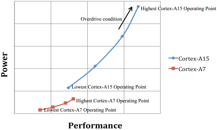
WTF is a flexible display for?
[48:53 – 54:00] of the video embedded in ‘Details’ section below:
How Microsoft is using Samsung components to enhance their solutions, Eric Rudder, chief technical strategy officer, Microsoft:
[51:37] We actually have a prototype of Windows Phone and how would look on one of those screens [51:41]
…


[51:41] And Microsoft’s vision is that sensors like Kinect combined with flexible, transparent and projected displays will bring us to a point when any object can be a Surface and can be a computer. I’d like to close with a short video from Microsoft Research which extends interactivity to every surface in your living room. Last year you’ve may seen some videos with precomputed projections. What we’re demoing today is both real-time and fully interactive. And while you may find it hard to believe the footage shown here is exactly what’ve appeared in the lab without any special effects being added. Some companies talk about reality distortion field we’ve actually built one. [52:32]
[52:35 – 53:20] IllumiRoom Projects Images Beyond Your TV for an Immersive Gaming Experience [MicrosoftResearch YouTube channel, Jan 8, 2013]
[53:24] This is just a glimpse of what our future may hold in store for us. We’re excited that this technology can be used in many different ways: to enhance a TV or movie experience, or increase the reality of a flight simulator, or make educational scenarios more exciting. We look forward to our continued partnership with Samsung to deliver the next generation of devices and services. [53:49]
Details
<CES 2013 “warm-up” clips, worth to skip> [3:10]
<Gary Shapiro intro, might be skipped> [6:00]
Samsung Exynos 5 Octa & Flexible Display at CES 2013 Keynote [SamsungTomorrow YouTube channel, Jan 9, 2012]
Samsung Highlights Innovations in Mobile Experiences Driven by Components, in CES Keynote [Samsung press release, January 9, 2013]
Samsung’s President Introduces Broader Partnerships, New Products and the Possibilities They Enable
LAS VEGAS–(BUSINESS WIRE)–Samsung Electronics Co., Ltd., a world leader in advanced semiconductor solutions, today redefined the story of consumer electronics from its perspective beneath the surface of mobile devices at the 2013 International CES keynote address.
“When you want multiple applications to perform at their best, you want the best application processor currently available—the Exynos 5 Octa.”
Dr. Stephen Woo, president of System LSI Business, Device Solutions Division, Samsung Electronics, shared the company’s vision of “Mobilizing Possibility,” highlighting the role of components as the engine behind innovation across the mobile landscape. The keynote event illustrated possibilities that Samsung envisions offering through its component solutions, and introduced new products that will herald such expectations.
“We believe the right component DNA drives the discovery of what’s possible,” said Woo. “Components are building blocks—the foundations on which devices are built. We at Samsung’s component solutions are creating new, game-changing components across all aspects of devices.”
Guests from partnering companies, such as Warren East, chief executive officer, ARM; Eric Rudder, chief technical strategy officer, Microsoft; Trevor Schick, senior vice president, enterprise group supply chain procurement, HP; and Glenn Roland, vice president and head of new platforms and OEM, EA; also took part in the event, echoing Samsung’s mission to offer breakthrough products and create shared value (CSV) for both manufacturers and end-users.
Woo opened by presenting Samsung’s goal for Mobilizing Possibility that takes big ideas off the drawing board and brings them to life for end-users, especially in the areas of processing performance, energy-efficient memory solutions and display technology. He emphasized that the limitless possibilities presented by consumer electronics will be based on component innovations by the company.
Processing Power
The first of Samsung’s new products announced at the keynote was the Exynos 5 Octa, the world’s first mobile application processor to implement the ARM® big.LITTLE™ processing technology based on the Cortex™-A15 CPU. Following the Exynos 5 Dual, which is already on board of market-leading products such as the Google Chromebook and Nexus 10, the successor is the newest addition to the Exynos family of application processors.
“The new Exynos 5 Octa introduces a whole new concept in processing architecture…designed for high-end smartphones and tablets,” said Woo. “When you want multiple applications to perform at their best, you want the best application processor currently available—the Exynos 5 Octa.”
To expand on the big.LITTLE concept, Warren East, chief executive officer, ARM, joined Woo on stage and introduced the new technology that has just become available in silicon through the Exynos 5 Octa. Housing a total of eight cores to draw from—four powerful Cortex-A15™ processors to handle processing-intense tasks along with four additional Cortex-A7™ cores for lighter workloads—the application processor offers maximum performance and up to 70 percent higher energy efficiency compared to the previous quad-core Exynos.
Glenn Roland, vice president and head of new platforms and OEM, EA [Electronic Arts], helped Woo demonstrate the processing power of the Exynos 5 Octa by showing off one of EA’s latest 3D racing games, Need for Speed™ Most Wanted. Atop the reference device, the application processor delivered an elevated real-life gaming experience within the mobile platform, rendering stunning graphics performance and real-time response speed.
Green Memory Capabilities
As advanced processing power on mobile devices accelerates easier data creation by the masses, the mobile experience will increasingly become more dependent upon datacenters largely responsible for the proliferating data traffic. Growing in size and capacity, IT systems face challenges both in performance and power savings to secure sustainability moving forward. Memory devices, the main products for servers that make up these datacenters, can deliver substantial gains by adopting cutting-edge technology available from Samsung.
Woo pointed out that managing the power consumption in these datacenters have become crucial and that Samsung’s green memory solutions with solid state drives (SSD) and advanced DRAM (dynamic random access memory) are addressing this key issue with their powerful, yet energy-efficient processing capabilities. Compared to traditional datacenters that incorporate hard disk drives (HDD), server and storage solutions equipped with green memory pull the data processing speeds up six-fold while operating with 26 percent less electricity.
Display Technology
As components on the surface that interact directly with users, display solutions bring the technology advancements to life and make them tangible through the device interface. Woo presented the future possibilities of Samsung’s displays along with Brian Berkeley, senior vice president of Samsung Display. While crystal-clear picture qualities become a reality, the two Samsung speakers were pleased to share that the innovations do not sacrifice energy efficiency.
Woo and Berkeley described the 10.1-inch liquid crystal display (LCD) panel that is currently adopted by the Nexus 10. With a 2560×1600 resolution and 300 pixels per inch (ppi), the panel renders stunning picture qualities while consuming only 75 percent of the energy used in previous display solutions.
Using Samsung’s energy-efficient green LCD technology, the company is currently developing a 10.1-inch model that would lower power consumption even further by 25 percent, while offering equal resolution qualities as its predecessor.
Prototypes and real-life scenarios for Samsung’s line of flexible organic light emitting diode (OLED) displays were also showcased, promising various mobile application opportunities for consumer electronics manufacturers. Dubbed “YOUM,” the flexible display line-up uses extremely thin plastic instead of glass, making it bendable and virtually “unbreakable.” Berkeley featured a smartphone prototype equipped with a curved edge that showed contiguous content along the side of the device.
“Our team was able to make a high-resolution display on extremely thin plastic instead of glass, so it won’t break even if it’s dropped,” said Berkeley. “This new form factor will really begin to change how people interact with their devices, opening up new lifestyle possibilities … [and] allow our partners to create a whole new ecosystem of devices.”
One of Samsung’s partners that bring the company’s state-of-the-art components together is Microsoft, adding more layers of value to the final product with its software solutions, devices and services. Eric Rudder, chief technical strategy officer, Microsoft, took the complete ATIV family of devices as an example through which Samsung’s component solutions and Windows 8 together present new potential in user interfaces. Rudder reported that Microsoft Research has been continuing its work on next-generation display technologies, enabling new modes of human-computer interaction.
Possibility for All
Creating a better world with its resources is one of Samsung’s core values. Samsung’s flagship corporate social responsibility initiative, Samsung Hope for Children, was launched in this spirit, through which the company provides its products, expertise and financial support to tackle the needs of children around the world for education and healthcare. Woo emphasized that Samsung’s innovation in components share the same thread as a driver that truly mobilizes possibility without boundaries or barriers.
“When [Samsung’s] technologies harmonize, amazing things happen. Advances in components are giving rise to a whole new era of possibility,” said Woo. “At Samsung, we are passionate about Mobilizing Possibility. Not just for the privileged few, but possibility for all.”
For more information about Samsung’s 2013 International CES keynote, visit www.samsung.com/2013ceskeynote or www.samsungces.com.
About Samsung Electronics Co., Ltd.
Samsung Electronics Co., Ltd. is a global leader in consumer electronics and the core components that go into them. Through relentless innovation and discovery, we are transforming the worlds of televisions, smartphones, personal computers, printers, cameras, home appliances, medical devices, semiconductors and LED solutions. We employ 227,000 people across 75 countries with annual sales exceeding US$143 billion. Our goal is opening new possibilities for people everywhere. To discover more, please visit www.samsung.com.
ARM TechCon 2012 – Warren East, CEO ARM Keynote [ARMflix, Nov 2, 2012]
More essential details:
– Cortex-A7 OR Low-Power Leadership for A Smarter Future – The Legend of ARM Cortex-A7 [USD 99 Allwinner, Jan 7, 2013]
– Fast 3d party IP OR the external Intellectual Property which makes Allwinner’s unprecedented pace of further next-gen SoC introductions possible despite of the company size of only 500 employees [USD 99 Allwinner, Dec 28, 2012]
– Samsung Exynos 5250 [Dec 6, 2011]
– for Samsung semiconductor foundry operation: see inside the Qualcomm’s critical reliance on supply constrained 28nm foundry capacity [this same ‘Experiencing the ‘Cloud’ blog, July 27 – Nov 13, 2012]
– Intel targeting ARM based microservers: the Calxeda case [this same ‘Experiencing the ‘Cloud’ blog, Dec 14, 2012]
– Intel’s biggest flop: at least 3-month delay in delivering the power management solution for its first tablet SoC [this same ‘Experiencing the ‘Cloud’ blog, Dec 20, 2012]
Windows RT must work with more chips to take off, ARM CEO says [CNET, Jan 9, 2012]
LAS VEGAS — Microsoft’s newest operating system that runs on cell phone chips is off to a slow start, but it’s only a matter of time before it gains more traction, the chief executive of chip technology designer ARM Holdings said.
Warren East, speaking today in an interview with CNET at the Consumer Electronics Show in Las Vegas, said that for that to happen, Microsoft needs to make its software, dubbed Windows RT, work with more ARM-based processors. He said it eventually will do so, but it’s unclear when that will be.
Currently, Windows RT runs only on Qualcomm and Nvidia chips (it also used to work with Texas Instruments’ processors, but that company decided to move away from providing chips for mobile devices). And only four PC makers ultimately built Windows RT products.
“If Microsoft wants to benefit from the ARM business model and the ARM world, then they’ll have to support multiple players,” East said. “Otherwise, there’s no real advantage for them in working with ARM.”
…
East today noted that when Microsoft first started talking with ARM about making a tablet/PC operating system that works with its processors, Microsoft wanted to work with only one ARM-based chip partner.
“We said, ‘no, no, you need to work with a few, because we have found over the years it helps to work with a few, or otherwise you end up getting too channeled into the requirements of one customer,” he said.
…
Microsoft Research at CES: IllumiRoom [Next at Microsoft blog, Jan 9, 2013]
Earlier this morning at CES, Eric Rudder, Microsoft’s Chief Technology Strategy Officer, joined the Samsung keynote to share Microsoft’s vision for extending computing interactions to any surface in your home. This wasn’t a product launch but I’m excited by the potential shown in the research that we shared.
Imagine a space like your kitchen or a classroom achieving that same level of interactivity as your phone – this will happen through a combination of embedded devices and sensors such as Kinect for Windows. Our research demo only covers educational and entertainment scenarios but the possibilities are endless.
It’s rare for a company to pull back the curtain and share research in such raw form at the world’s largest technology tradeshow. However, we think it’s vitally important to get the next generation of students excited about Computer Science – and what better way than to show off research that makes gaming more fun!
While magicians never share their secrets, researchers have to publish, so, a bit of explanation about the demo is in order. You may have seen interesting 3D-mapped projections over the past few years – Microsoft partners like Nokia and Samsung have both used pre-rendered footage in recent marketing efforts. What’s new in this work is that our researchers used Kinect for Windows to map the room in real-time in order to make projected illusions fully interactive. Most importantly, the effects shown in the video were captured live as they appeared in the living room environment and are not the result of special effects added in post processing.
For more on the science behind this demo, check out the MSR IllumiRoom project site from Hrvoje Benko, Andrew Wilson, Eyal Ofek, and Brett Jones – they’ll have more to come at CHI 2013 in April.
IllumiRoom: Peripheral Projected Illusions for Interactive Experiences [Microsoft Research, Jan 9, 2013 ]

IllumiRoom is a proof-of-concept system from Microsoft Research. It augments the area surrounding a television screen with projected visualizations to enhance the traditional living room entertainment experience.
IllumiRoom uses a Kinect for Windows camera and a projector to blur the lines between on-screen content and the environment we live in allowing us to combine our virtual and physical worlds. For example, our system can change the appearance of the room, induce apparent motion, extend the field of view, and enable entirely new game experiences.
Our system uses the appearance and the geometry of the room (captured by Kinect) to adapt the projected visuals in real-time without any need to custom pre-process the graphics. What you see in the videos below has been captured live and is not the result of any special effects added in post production.
Stay tuned for more information and a paper explaining all the details coming up at ACM CHI 2013.

Intel targeting ARM based microservers: the Calxeda case
- Intel Atom processor S1200 vs. Calxeda ECX1000 for microservers
- ARM Holdings on the server opportunity
- x86 on ARM with Linux
- Boston Ltd. related information from Calxeda
- Background on Elbrus (in Russian or English if available)
- Background on Elbrus Technologies (in Russian)
See also:
– Binary translation [Wikipedia, Sept 2, 2012]
– Calxeda [Wikipedia, Nov 12, 2012]
– Microserver (Server appliance) [Wikipedia, Nov 5, 2012]
Intel Atom processor S1200 vs. Calxeda ECX1000
for microservers
Intel Delivers the World’s First 6-Watt Server-Class Processor [Intel press release, Dec 11, 2012]
Several Equipment Makers Building Microservers, Storage and Networking Systems Based on 64-bit Intel® Atom™ Processor S1200 Product Family
NEWS HIGHLIGHTS
- Intel® Atom™ processor S1200 server system on-chip hits lower-power levels, and includes key features such as error code correction, 64-bit support, and virtualization technologies required for use inside data centers.
- More than 20 low-power designs including microservers, storage and networking systems use the Intel Atom processor S1200 family.
Intel Corporation introduced the Intel® Atom™ processor S1200 product family today, delivering the world’s first low-power, 64-bit server-class system-on-chip (SoC) for high-density microservers, as well as a new class of energy-efficient storage and networking systems. The energy-sipping, industrial-strength microprocessor features essential capabilities to achieve server-class reliability, manageability and cost effectiveness.
“The data center continues to evolve into unique segments and Intel continues to be a leader in these transitions,” said Diane Bryant, vice president and general manager of the Datacenter and Connected Systems Group at Intel. “We recognized several years ago the need for a new breed of high-density, energy-efficient servers and other datacenter equipment. Today, we are delivering the industry’s only 6-watt1 SoC that has key datacenter features, continuing our commitment to help lead these segments.”
Intel’s Next Generation of Microservers: The Real Thing
As public clouds continue to grow, the opportunity to transform companies providing dedicated hosting, content delivery or front-end Web servers are also growing. High density servers based on low-power processors are able to deliver the desired performance while at the same time significantly reduce the energy consumption – one of the biggest cost drivers in the data center. However, before deploying new equipment in data centers, companies look for several critical features.
The Intel Atom processor S1200 product family is the first low-power SoC delivering required data center features that ensure server-class levels of reliability and manageability while also enabling significant savings in overall costs. The SoC includes two physical cores and a total of four threads enabled with Intel® Hyper-Threading Technology2 (Intel® HT). The SoC also includes 64-bit support, a memory controller supporting up to 8GB of DDR3 memory, Intel® Virtualization Technologies (Intel® VT), eight lanes of PCI Express 2.0, Error-Correcting Code (ECC) support for higher reliability, and other I/O interfaces integrated from Intel chipsets. The new product family will consist of three processors with frequency ranging from 1.6GHz to 2.0GHz.
The Intel Atom S1200 product family is also compatible with the x86 software that is commonly used in data centers today. This enables easy integration of the new low-powered equipment and avoids additional investments in porting and maintaining new software stacks.
New Milestones in Power Efficiency
Intel continues to drive power consumption down in its products, enabling systems to be as energy efficient as possible. Each year since the 2006 introduction of low-power Intel® Xeon® processors, Intel has delivered a new generation of low-power processors that have decreased the thermal design power (TDP) from 40 watts in 2006 to 17 watts this year due to Intel’s advanced 22-nanometer (nm) process technology. The Intel Atom processor S1200 product family is the first low-power SoC with server-class features offering as low as 6 watts1 of TDP.
Broad Industry Support
Today, more than 20 low-power designs including microservers, storage and networking systems use the Intel Atom processor S1200 processor family from companies including Accusys*, CETC*, Dell*, HP*, Huawei*, Inspur*, Microsan*, Qsan*, Quanta*, Supermicro* and Wiwynn*.
“Organizations supporting hyperscale workloads need powerful servers to maximize efficiency and realize radical space, cost and energy savings,” said Paul Santeler, vice president and general manager, Hyperscale Business Unit, Industry-standard Servers and Software at HP. “HP servers power many of those organizations, and the Intel Atom processor S1200 will be instrumental as we develop the next wave of application-defined computing to dramatically reduce cost and energy use for our customers.”
An Even Brighter Future
Intel is working on the next generation of Intel Atom processors for extreme energy efficiency codenamed “Avoton.” Available in 2013, Avoton will further extend Intel’s SoC capabilities and use the company’s leading 3-D Tri-gate 22 nm transistors, delivering world-class power consumption and performance levels.
For customers interested in low-voltage Intel® Xeon® processor models for low-power servers, storage and networking, Intel will introduce the new Intel Xeon processor E3 v3 product family based on the “Haswell” microarchitecture next year. These new processors will take advantage of new energy-saving features in Haswell and provide balanced performance-per-watt, giving customers even more options.
Pricing and Availability
The Intel Atom processor S1200 is shipping today to customers with recommended customer price starting at $54 in quantities of 1,000 units.
More information on the announcement including Diane Bryant’s presentation, additional documents and pictures are available at http://newsroom.intel.com/docs/DOC-3172.
Fact Sheets & Backgrounders
See also:
Intel® Atom™ Processor S1200 for Microserver: Datasheet, Vol. 1 [Intel, Dec 2012]
Comparing Calxeda ECX1000 to Intel’s new S1200 Centerton chip [‘ARM Servers Now’ blog from Calxeda, Dec 11, 2012]
Based on what Intel disclosed today, here’s a snapshot of Calxeda EnergyCore 1000 vs. Intel’s new S1200 chip
ECX1000
Intel S1200
Watts
3.8
6.1
Cores
4
2
Cache (MB)
4 Shared
2 x .5 MB
PCI-E
16 lanes
8 lanes
ECC
Yes
Yes
SATA
Yes
No
Ethernet
Yes
No
Management
Yes
No
OOO Execution
Yes
No
Fabric Switch
80 Gb
NA
Fabric ports
5
NA
Address Size
32 bits
64 bits
Memory Size
4 GB
8 GB
So, while the Centerton announcement indicates that Intel takes “microservers” seriously after all, it falls short of the ARM competition. It DOES have 64-bits and Intel ISA compatibility, however. Most workloads targeting ARM are interpreted code (PHP, LAMP, Java, etc), so this is not as big a deal as some would have you believe! Intel did not specify the additional chips required to deliver a real “Server Class” solution like Calxeda’s, but our analysis indicates this could add 10 additional watts PLUS the cost. That would imply the real comparison is between ECX and S1200 is ~3.8 vs ~16 watts. So roughly 3-4 times more power for Intel’s new S1200, again, comparing 2 cores to 4. Internal Calxeda benchmarks indicate that Calxeda’s four cores and larger cache delivery 50% more performance compared to the 2 hyper-threaded Atom cores. This translates to a Calxeda advantage of 4.5 to 6 times better performance per watt, depending on the nature of the application.
What is a “Server-Class” SOC? [‘ARM Servers Now’ blog from Calxeda, Dec 12, 2012]
As reported in various outlets yesterday, Intel has released their S1200 line of Atom SOC’s targeting the microserver market with the tagline: “Intel Delivers the World’s First 6-Watt Server-Class Processor”. The first notable point here is that they had to use 6 Watts, because 5 was already taken. The second notable point is their definition of “Server-Class”. Looking at the list of features on the Atom S1200, there are key “Server-Class” features missing:
- Networking: Intel’s SOC requires you to add hardware for networking
- Storage: Once again, there is no SATA connectivity included on the Intel SOC, so you must add hardware for that
- Management: Even microservers need remote manageability features, so again with Intel you need to tack that on to the power and price budgets.
Unless you add additional hardware on top of it, Intel’s SOC allows you to boot and not much else. Let’s also consider the fact that you’ve got a total of 8 lanes of PCI Express Gen 2 on each SOC. If you’d like to add the Server-Class items listed above, choose wisely, because those 8 lanes will go fast. Add all of that hardware, plus memory, and 6 W is simply not possible. And of course these additional components add cost and take space as well.
Let’s expand that thought to an actual Atom S1200 powered system, like the Quanta S900- X31A. Each node includes a Marvell 88SE9130 SATA controller at a TDP of 1W, an Intel i350 1GB controller at 2.8W TDP, an AST2300M estimated at a conservative 1W, and an SODIMM at roughly 1.2W (Using the same number we at Calxeda have used). That adds at least 6 more watts per node, almost doubling the 6.1W TDP of the processor. Multiply that across 48 nodes and you just tacked on 288W to each chassis. In a 42U rack full of them, you just added 4kW to each rack! By no means is that a limitation or shortcoming of the Quanta design, which is actually quite good, but rather an indication of the excess baggage that all vendors will need to deal with in putting together an S1200 powered system.
The [Ultimate Data X1 (UDX1) system from Penguin Computing] currently [the Viridis from Boston] shipping [the SystemFabricCore from System Fabric Works] Calxeda ECX-1000 Server-Class SOC ships with SATA, Ethernet fabric links, IPMI-based management, and 8 lanes of PCI Express Gen 2, standard at 3.8W (5W including 4GB DDR3). It’s also worth pointing out that Calxeda’s integrated fabric switch provides more than just the Ethernet ports missing on the Atom S1200. Applied at the system and rack level, it can dramatically reduce Top of Rack Switch ports and cabling complexity, while increasing internode bandwidth by 10-fold. You can have all of that in a 5W server. Not 5W + additional components. Why not take that 12W budget you need for each S1200 node and get two Calxeda nodes with all of the Server-Class features included?
In the end, Intel may simply be claiming 64-bit as the main benchmark for Server-Class. When matching microservers to the appropriate workloads, we’ve found that there is surely a place for 32-bit in the datacenter. We’ll be providing a blog post on that very topic in the near future.
Penguin Computing’s New High Density System Ultimate Data X1 Brings ARM’s Low-power Footprint To The Data Center [Penguin Computing press release, Oct 17, 2012]
Penguin Computing today announced the immediate availability of its Ultimate Data X1 (UDX1) system. The UDX1 is the first server platform offered by a North American system vendor that is built on the ARM®-based EnergyCore System on Chip (SoC) from Calxeda.
The UDX1 brings new levels of efficiency and scale to internet datacenters. With a five Watt power envelope per server the UDX1 is ideal for I/O bound workloads including “Big Data” applications, scalable analytics and cloud storage. The UDX1 offers a drastic reduction of TCO for high-density, low power computing environments. Workloads that have been processed by racks of conventional systems can now be handled by a group of servers in a single physical unit. The UDX1 features a modular architecture that can be configured with up to 48 Calxeda EnergyCore server nodes, with four cores per node. The system includes an internal 10 Gigabit Ethernet switch fabric for node-to-node connectivity and provides up to 144TB of hard drive capacity.
“Power and cooling are the biggest facility challenges for most data centers, on the other hand typical cloud computing, web 2.0 and ‘Big Data’ applications are based on scale out architectures,” said Charles Wuischpard, CEO of Penguin Computing.“A new generation of power efficient high density servers is required to run these workloads efficiently. With the incredibly low power envelope and the extremely high density Calxeda’s EnergyCore SoCs offer, the UDX1 is the ideal platform for running these types of workloads.”
“Penguin is an innovator in Linux based solutions for internet datacenters and high performance computing. We are thrilled that their next generation of innovative products includes Calxeda,” said Barry Evans, CEO Calxeda. “We are realizing this new era in breakthrough low power computing that will lift the constraints on datacenter performance and efficiency. Penguin is helping chart this course with an ideal solution to span from scale-out cloud storage to analytics.”
Penguin Computing will be showing a live demo of Hadoop running on the UDX1 at the upcoming Strata Conference + HadoopWorld on October 24-25 in New York.
For more information, please visit www.penguincomputing.com.About Penguin Computing
For well over a decade Penguin Computing has been dedicated to delivering complete, integrated Enterprise and High Performance Computing (HPC) solutions that are innovative, cost effective, and easy to use. Penguin offers a complete end-to-end portfolio of products and solutions including workstations, rack-mount servers, custom server designs, power efficient rack solutions and turn-key clusters. Penguin also offers the Scyld suite of software products for efficient provisioning and infrastructure monitoring. For users who want to use supercomputing capabilities on-demand and pay as they go, Penguin provides Penguin Computing on Demand (POD), a public HPC cloud that is available instantly and as needed.
Penguin counts some of the world’s most demanding organizations as its customers, including Yelp, Caterpillar, Life Technologies, Dolby, Lockheed Martin and the US Air Force. Penguin Computing is a registered trademark of Penguin Computing, Inc. Penguin Computing on Demand is a pending trademark in the US. All other trademarks are property of their respective owners. Other product or company names mentioned may be trademarks or trade names of their respective companies.
Boston Viridis – ARM® Microservers [Boston product page, Oct 18, 2012]
It was announced at ISC 2012 on June 13, 2012 with whitepaper released simultaneously.
THE WORLD’S FIRST HYPERSCALE SERVER

Hyperscale Computing represents an inflexion point in the industry that will disrupt the very concept of a server in future systems. Modern servers have come a long way, but they are nonetheless fundamentally based around designs originally created decades ago.
The Boston Viridis is a self contained, highly extensible, 48 node ultra-low power ARM® cluster with integral high-speed interconnect and storage within a standard single 2U rack mount enclosure.
Racks of individually connected, high-power, low density servers and blades are installed in modern data centres thousands at a time. Each of these server systems requires its own networking infrastructure, high power distribution, HVAC, and maintenance engineers to take care of it when things go wrong. These ineffciencies could cost data centres billions.
The Boston Viridis uses Server-on-Chip (SoC) technology to integrate the CPU (powered by ARM®), networking and IO onto the server chip. SoC technology, which began life as an embedded systems technology but is primed to storm the data centre in the next few years allows for mass levels of integration at high density requiring little active cooling. With this technology today we can now con gure over a thousand servers in a standard 42U rack.
The Boston Viridis uses the ARM® -based Calxeda EnergyCore® to create a rack mountable 2U server cluster. The solution comprises of 192 processing cores leading the way towards energy effcient hyperscale computing.
Each 2U chassis contains a total of 12 Calxeda EnergyCards connected to a common mainboard sharing power and fabric connectivity. The Calxeda EnergyCard is a single PCB module containing 4 Calxeda EnergyCore SoCs; each with 4GB DDR-3 Registered ECC Memory, 4 x SATA connectors and management interfaces.
Ethernet switching is handled internally by 80Gb bandwidth on the EnergyCore fabric switch, thereby negating the need for additional switches that consume unnecessary power and add unwanted latency.
Astonishingly, utilising all 48 Calxeda EnergyCore SoCs, the whole package including fabric and management consumes less than 300W – this is achieved as each SoC device consumes just 0.5 to 5 watts of power (depending on load).
With specific applications, the overall combined performance of one 2U Boston Viridis appliance can outperform a whole rack of standard x86 servers, yet at the same time consume 1/10th the power and occupy 1/10th the space making it an excellent investment for datacentres and enterprises alike.
SystemFabriCore [product page from System Fabric Works, Nov 30, 2012]
It was announced at SC12 on Nov 12, 2012 with demonstration at the Calxeda booth.
The First, and Next Step in Hyper-Efficient Computing
The SystemFabriCore is an Ultra Dense, Ultra Low Power Computing Platform based on a revolutionary new approach to highly parallel, densely packaged, tightly integrated systems utilizing the Calxeda EnergyCore™ SOC (System on a Chip) which delivers computing, fabric, network, storage I/O and management, all in one 3.8 watt SOC as opposed to a traditional x86 motherboard based architecture using 100s of watts.

The SystemsFabriCore is a self contained, highly extensible, multi-node cluster with integral high- speed interconnect and storage within a standard 2U rackmount enclosure.
- Available up to 48 SoC components delivered on 12 Calxeda EnergyCard platforms
- Each Calxeda EnergyCore™ SoC contains a quad-core processing unit, providing a total of 192 cores per 2U enclosure
- 24 x 2.5” SATA HDDs or SSD devices
- 4 x 4GB miniDIMM modules per EnergyCard, providing a total of 192GB of RAM per 2U enclosure
- Rear I/O supporting 4 x SFP+ cages for external fabric connectivity (1Gbe or 10Gbe depending on configuration and number of Energy Cards) and 1 x serial port for management.

FEATURES:
- Easily scalable to thousands of nodes
- Calxeda EnergyCore™ SoC Redefines Big Data Efficiency
- Each EnergyCore™ contains an ARM® Cortex™-A9 Quad-core CPU
- Up to 10X the performance in the same power and space
- Cuts energy use and space by up to 90%
- Industry leading low power consumption 3.8 watts per SoC
- Up to 24 SATA HDDs or SSD per 2U
- Up to 192GB of RAM per 2U enclosure
- Total of 192 cores per 2U


ARM Holdings on the server opportunity
ARM in Servers: Taming Big Data with Calxeda @ ISC’12 [ARM Holdings’ Smart Connected Devices blog, June 18, 2012]
I spent a number of years working in High Performance Computing (HPC) and found it to be one of the most innovative communities I’ve had the pleasure to work with. That’s why I’m certain they’re going to be excited to see and hear what Calxeda, an ARM® Connected Community®partner, has to offer at ISC’12 this week! Spoiler alert: they’ll be sharing some new performance and Total Cost of Ownership (TCO) data that shows just how compelling a right-sized solution can be for the target workloads. And what do I mean by ‘right-sized’ solution? More on that in a moment…
First, I’d like to offer kudos to the HPC community for tackling some of the largest and most complex problems known. Unsung heroes in so many aspects of our everyday life – for example, have you ever wondered how cars continue to get safer and more efficient each year? (Hint: they use lots of computers to model and simulate scenarios to improve safety and efficiency.) Similar techniques are used to uncover new medicines, forecast weather, identify new energy sources and predict future environmental impacts to name just a few. Then there’s ‘Big Data’ which applies HPC-like techniques to mine the ever-increasing sources and quantities of unstructured data (search queries, social media, financial transactions, crime reports, live traffic, smart meters etc…) for seemingly unrelated but extremely interesting (read: valuable) patterns and insight.
To tackle a large project, you typically break it down into smaller manageable chunks. In the case of HPC and Big Data, that means decomposing and distributing data across many servers (think hundreds and in some cases thousands or even tens of thousands), then collecting and consolidating the results into an overall ‘solution.’ Today, this is typically performed using a technique such as MapReduce enabled by software from companies like Cloudera, Datastax, MapR and Pervasive running on a cluster of general-purpose servers connected via high-performance networks. Often the compute requirements are somewhat modest relative to the enormity of the data, meaning unimpeded data movement is fundamental to overall efficiency.
With that as a backdrop, think for a moment – “how would you architect highly efficient servers for this purpose if you had a clean slate?” ARM’s business model enables innovative companies the freedom and choice to do just that, resulting in highly efficient and targeted solutions.
As stated before, one size no longer fits all.
To achieve a step function in efficiency, often requires new thinking. In the case of data intensive computing, re-balancing or ‘right-sizing’ the solution to eliminate bottlenecks can significantly improve overall efficiency. That’s exactly what Calxeda has done with its EnergyCore™ ECX-1000 series processor. By combining a quad-core ARM®Cortex™-A series processor with topology agnostic integrated fabric interconnect (providing up to 50Gbits of bandwidth at latencies less than 200ns per hop), they can eliminate network bottlenecks and increase scalability. EnergyCore also includes all the traditional server I/O, memory and management interfaces you would expect. This ‘just add memory’ server on a chip approach means servers can literally be credit card sized and operate at a power-sipping 5W of total power. That means huge density increases are also possible: –
Click here for more details on the Calxeda EnergyCore ECX-1000 SoC.
With all this innovation, it’s easy to get caught up in the hardware, but we also need to recognize software plays an important role here. While the ecosystem is coming together quite nicely with Canonical’s Ubuntu Server 12.04LTS release and various open source libraries already available, there’s still much work ahead. As of today, the fundamental pieces are in place to begin doing useful work and key software partners are already engaged with Calxeda on early access hardware. Forthcoming availability of ARM processor-based server systems fromHP and other OEMs will accelerate the next phase of software ecosystem developments.
If you’re at ISC’12 this week and want to know more, be sure to visit Calxeda at booth #410, and check out Karl Freund’s speaking session on the show floor Tuesday, June 19th at 4:15pm. If you’re not at ISC’12 we’ll also be at SC’12 in November (booth #122.) But trust me you don’t want to be left waiting until then! There are plenty of other opportunities throughout June (including GigaOM Structure 2012 in San Francisco.) And we’ll be announcing more opportunities to meet the Calxeda and ARM teams in the near future so be sure to watch this space!
Jeff Underhill, Server Segment Marketing Manager, ARM, is based in Silicon Valley. After spending 10+ years working in the traditional server market Jeff saw an opportunity to revisit server design and redefine an industry. ARM’s business model enables innovative companies the freedom and choice to ask themselves “how would I architect highly efficient servers if I had a clean slate?” Consequently, he is helping drive ARM’s server program with a view to redefining the boundaries of traditional servers as opposed to simply replacing incumbent platforms.


ARM Cortex-A50: Broadening Applicability of ARM Technology in Servers [ARM Holdings’ Smart Connected Devices blog, Oct 31, 2012]
I have been running the ARM® server initiative for a little over four years. At kickoff, there were few that believed that ARM technology would find its way into server applications. Fast forward to today, more of the strands of the strategy are now in the public domain.
- 32-bit ARM powered platforms, from companies that include Boston, Dell, HP, Mitac and Penguin Computing (based on either Marvell’s or Calxeda’s EnergyCore system-on-chip devices) are starting to ship into the market. Customers can start to evaluate the performance of their workloads on ARM based servers hosted in the cloud.
- The initial pieces of the software ecosystem are starting to appear including performance optimized Java compilers/java virtual machines, commercial grade Linux distributions and application stacks.
For companies developing businesses based on web infrastructure, the server IS the business. These companies have honed their software and hardware strategies to enable quick adoption of technologies that drive down system acquisition costs or running costs. Increased use of open source software on a Linux platform reduces the legacy ties to incumbent server platforms and paves the way for more innovation. Companies are now making decisions on system technologies based on metrics like performance (on the user application) / watt / $ or performance / watt / foot3 as opposed to the pure performance.
ARM has consistently indicated that a relatively small set of server applications could take advantage of a 32-bit ARM processor and that the availability of 64-bit ARM devices would significantly broaden the applicability. In the cloud infrastructure space, the main benefit that the 64-bit execution state brings is access to a larger memory address space. 2014 will be the year when we see 64-bit ARM powered server SoCs appearing in the market. Now surely those will all be based on the ARM CortexTM-A57, right? Well, what we have learnt in the server journey is that one size does not fit all. Some server workloads do benefit from a high single thread performance. However, as Brian Jeff notes in his blog [see big.LITTLE in 64-bit, also copied here just below], for applications that have modest compute requirements, the Cortex-A53 processor will deliver the best throughput performance inside a specific power envelope.
We think our cores are a great base for server devices. But as important is the ARM business model which enables our silicon licensees to tightly couple peripherals, memory and processing engines of the same piece of silicon. The selection of this mix of functionality that balances the compute, networking and storage elements for the specific server application is key to driving advantages in the metrics discussed above.
But a chip is useless without software. Earlier this year, ARM released a 64-bit Linux distribution and tools into the open source community. The primary focus of my team is to ensure the multiple commercial grade Linux distributions pick up this technology, augmented with virtualization and application stacks, all in time to intersect silicon availability. Fortunately, we have an early pioneer in in the ARMv8 space. At ARM TechconTM 2011, Applied Micro announced their intent to develop a 64-bit ARM powered server device. ARM demands compatibility between companies that develop their own ARM processors (achieved through an architecture license) and cores that ARM licenses. Software companies are already developing software for use on ARMv8 processors using an FPGA version of the Applied Micro’s X-Gene device. This will be superseded with real silicon, set to appear in the early part of 2013. You can expect to see more announcements about the progress regarding 64-bit server software in the coming quarters.
Some observers remain skeptical as to ARM’s likelihood of success here. My team is immersed daily in this engagement so it is fair to say we are somewhat passionate and evangelical about our chances. What I think we can agree on is that the announcement of the Cortex-A50 series removes a technical barrier that many have argued prevent ARM’s access into the server domain. The list of lead partners of these cores, such as AMD and Calxeda, augmented with the three publically announced ARMv8 architecture licensees (Applied Micro, Cavium and NVIDIA) is an early indicator that choice is coming to the server domain. One size does not fit all. The winners will be those that best deliver relevant, compelling functionality alongside the processor core. A space long devoid of innovation is about to undergo some significant disruption!
Ian Ferguson, Director of Server Systems and Ecosystem, ARM,has spent years fighting from the corner of the underdog. Most of those scars are healing nicely. Ian is particularly passionate about taking ARM technology into new types of applications that do not exist or are at the very formative stages. Consequently, he is driving ARM’s server program with a view to reinvent the way the server function is implemented in networks as opposed to simply replacing incumbent platforms.
big.LITTLE in 64-bit [ARM Holdings’ SoC Design blog, Nov 1, 2012]
With the ARM® CortexTM-A50 series processors, ARM has introduced a “big” and “LITTLE” processor pair that is 64-bit capable. So with this 2nd generation of big.LITTLE platform, what does this mean for big.LITTLE software, which is currently being readied for deployment on ARMv7 32-bit processors? How will big.LITTLE processing technology be used in applications outside mobile like low-power servers, where 64-bit processing is a growing requirement?
Preparing for 64b Operating Systems
To start with, I should highlight that big.LITTLE software operates at the level of the operating system, in kernel space. To be clear, this means it is completely transparent to all apps and middleware. In both the major modes of operation (CPU migration and big.LITTLE MP) (discussed in more detail elsewhere) the software consists of a relatively small patch set to the OS kernel. Today, these patches are written in ARMv7 code, available in the open source or from Linaro. The Cortex-A50 series processors support the AArch32 execution state which is 100% backward compatible with ARMv7, so a Cortex-A50 series big.LITTLE processor can run existing 32-bit kernels without any major changes, including kernels that have been patched to support big.LITTLE. There will be some changes in cache maintenance routines, but effectively the big.LITTLE software is the same.
This is important as we are continuously improving the ARMv7 big.LITTLE code base. The first generation of devices based on big.LITTLE processors expected in the market in 2013.
ARMv8 allows 64-bit and 32-bit operation. AArch64 is the architecture that describes 64-bit mode of operation and AArch32 describes the 32-bit mode of operation. AArch64 also delivers other architectural benefits like enhanced SIMD, larger register files, enhanced cache management, tagged pointers, and more flexible addressing modes. For a big.LITTLE processor to deliver the architectural benefits of AArch64, it must run a 64-bit OS built on AArch64.
ARM 64-bit Linux has already been up-streamed, and ARM has demonstrated Android 32-bit code running (unmodified) on top of the 64-bit Linux kernel. The next step in providing big.LITTLE support in the 64-bit kernel is to modify the big.LITTLE MP and CPU migration patch sets to work cleanly in the AArch64 environment. Fortunately the code is not strongly impacted by register width, and therefore the vast majority should port cleanly and with little effort from ARMv7 to 64 bit; we plan to do this work at ARM and release 64-bit capable patch sets in mid-2013. This lines up well with expected Cortex-A50 based SoCs sampling at the end of 2013 and deployed in products in 2014.
Although we don’t expect 64-bit mobile OS’s to become prevalent that early, the AArch32 mode of the Cortex-A50 series processors will handle the ARMv7 32b OS, and will be ready for the transition to 64-bit when it does occur.
big.LITTLE in the Enterprise?
Originally conceived as an energy savings technique for mobile phones, big.LITTLE can be viewed as an interesting disruptive technology for applications like ARM processor based low-power servers. For servers and networking applications which are generally memory bound, having a large number of efficient processors that are tuned to workload makes a lot of sense. Often this workload leads itself to having multiple cores at different performance levels, but which are software identical.
As performance scales to higher core counts and the system power budgets reduce, the amount of power budget left for the CPU even in enterprise is very similar to that of mobile. Consider a fanless 20-25 W chip that has 16 CPUs, IO devices, a large L3 cache and other accelerators on board. Once you strip out the budgets for the non-CPU portions and split the remaining amongst the 16 CPUs, they budget is very much similar to a mobile phone power budget. big.LITTLE allows system designers to have their cake and eat it by delivering enterprise performance using a mobile pedigree processors and resultant low-cost, fanless device.
The other aspect of big.LITTLE technology that is attractive is the ability to more efficiently support a dynamically varying level of required performance. Infrastructure equipment is typically designed for the peak operating capacity, for example, to support the call volume on Mother’s Day or the mobile internet traffic during the Super Bowl. On most days the traffic is at most half of the peak traffic. An architecture that includes a mix of big and LITTLE cores in the same system, or even on the same die, can be dynamically adapted to the performance needs of the network more efficiently. This leads to better overall power consumption and reducing TCO.
big.LITTLE MP software, which gives the OS full view of all the big and LITTLE processors in the system, can automatically handle the work allocation in such a system. This mode of scheduling is more appropriate to the enterprise use case than CPU migration. CPU migration leverages dynamic voltage and frequency scaling (DVFS) to trigger the move between big and LITTLE cores. This works well in mobile devices which typically employ DVFS, but is not as suitable for enterprise systems which typically do not. Now that big.LITTLE MP has been effectively demonstrated on real silicon, enterprise partners are evaluating how big.LITTLE can help them achieve their performance goals without blowing the power budget.
In servers, the benefits of big.LITTLE are still under investigation. There is tremendous interest in ARM based low-power servers, where even our “big” Cortex-A57 CPU will consume significantly lower power than incumbent solutions. With increasing pressure on OEMs to create power efficient servers, it is clear that high peak performance CPUs do not always equate to the best solution. One CPU size does not fit all. For many classes of server solutions, aggregate throughput is more important than peak performance. In these applications, a many core approach with lots of LITTLE Cortex-A53 processors delivers the highest level of aggregate performance under a reduced power budget. It is likely that a range of power efficient server products will be built around Cortex-A57 or Cortex-A53, but probably not with both on the same chip. The OS software will be ready to cope with either case, big.LITTLE or homogenous multi-core, as the market evolves.
Brian Jeff, Product Manager at ARM, is based in Austin. Brian focuses on the power efficient vector along ARM’s application processor roadmap, including the Cortex-A5, the newly introduced Cortex-A7, and other CPUs further down the roadmap. He has also focused on benchmarking, performance analysis, and power analysis for ARM CPUs and systems. Brian joined ARM 3 years ago; prior to joining ARM he spent time at Texas Instruments and Freescale Semiconductor in product marketing, product management, and applications engineering roles. He has an MBA from the University of Texas at Austin and a BSEE from Virginia Tech.
x86 on ARM with Linux
Here comes the emulators! (EE Times Article) [‘ARM Servers Now’ blog from Calxeda, Oct 3, 2012]
Remember how smoothly Apple transitioned from PowerPC chips to X86 back in the mid 2000′s? Customers hardly noticed that all their software “just worked” on a completely different ISA, thanks to some cool software built by “Transitive”, a small UK based company since gobbled up by IBM. Well, emulation doesn’t solve ALL the worlds problems, and critical applications will of course need to go native for maximum performance. But this approach can be very helpful with the CAO, or Computer Aided Other; the ancillary but important applications, tools, and utilities that are so pervasive in a datacenter.
Below is an excerpt from the EE Times article, ARM Gets Weapon in Server Battle Vs. Intel.
Russian engineers are developing software to run x86 programs on ARM-based servers. If successful, the software could help lower one of the biggest barriers ARM SoC makers face getting their chips adopted as alternatives to Intel x86 processors that dominate today’s server market.
Elbrus Technologies has developed emulation software that delivers 40 percent of current x86 performance. The company believes it could reach 80 percent native x86 performance or greater by the end of 2014. Analysts and ARM execs described the code as a significant, but limited option.
A growing list of companies–including Applied Micro, Calxeda, Cavium, Marvell, Nvidia and Samsung-aim to replace Intel CPUs with ARM SoCs that pack more functions and consume less power. One of their biggest hurdles is their chips do not support the wealth of server software that runs on the x86.
The Elbrus emulation code could help lower that barrier. The team will present a paper on its work at the ARM TechCon in Santa Clara, Calif., Oct. 30-Nov. 1.
The team’s software uses 1 Mbyte of memory. “What is more exciting is the fact that the memory footprint will have weak dependence on the number of applications that are being run in emulation mode,” Anatoly Konukhov, a member of the Elbrus team, said in an e-mail exchange.
The team has developed a binary translator that acts as an emulator, and plans to create an optimization process for it.
“Currently, we are creating a binary translator which allows us to run applications,” Konukhov said. “Implementation of an optimization process will start in parallel later this year–we’re expecting both parts be ready in the end of 2014.”
…
Work on the software started in 2010. Last summer, Elbrus got $1.3 million in funding from the Russian investment fund Skolkovo and MCST, a veteran Russian processor and software developer. MCST also is providing developers for the [Elbrus] project. Emulation is typically used when the new architecture has higher performance than the old one, which is not the case-at least today–moving from the x86 to ARM. “By the time this software is out in 2014 you could see chips using ARM’s V8, 64-bit architecture,” Krewell noted. “That said, you will lose some of the power efficiency of ARM when doing emulation,” Krewell said. “Once you lose 20 or more percent of efficiency, you put ARM on par with an x86,” he added. Emulation “isn’t the ideal approach for all situations,” said Ian Ferguson, director for server systems and ecosystem at ARM. “For example, I expect native apps to be the main solution for Web 2.0 companies that write their own code in high level languages, but in some areas of enterprise servers and embedded computing emulation might be interesting,” he said.
Russian Chip Gurus ARM Intel Rivals With Secret Weapon [Wired, Oct 5, 2012]
Elbrus was founded in 2010 by employees of MCST — the company behind the Russian computer system also called Elbrus. In 2012, MCST and the Russian investment fund Skolkovo invested $1.3 million into the new Elbrus Technologies.
At MCST, the startup team was part of the Binary Translation Department building x86 emulators for the Russian microprocessor E2K. According to Konukhov, their emulator performed 85 percent as well as native code. They also took part in a joint project with Intel to develop an x86 translator for Intel’s Itanium chip that achieved 90 percent of native performance. Konukhov says that MCST has published 46 journal articles on binary translation, and that the company has several USA patents in the field.
Elbrus Technology’s secret sauce is its binary translator with multiple layers of hand-tuned optimization. And all the translations are handled in memory to speed up the process, with the translator itself taking up just 1MB of memory.
Although the goal is to reach 80 percent of the performance of native ARM, Knukhov says stability is more important. “Our marketing research clearly shows that most vendors and users are interested in functionality and stability rather then performance,” he says. “It is possible for us to release our solution without fully reaching performance goals and enhancing it afterwards.”
Linux 3.7 оправдал надежды ARM-разработчиков [PC Week/Russian Edition, 13.12.2012]
…
Российская компания “Эльбрус Технологии”, разработчик микропроцессоров, готовится решить эту проблему. Компания ведет разработку эффективного эмулятора для запуска x86-приложений на ARM-оборудовании. Данная разработка сейчас находится в стадии альфа-версии. Компания намерена к 2013 г. выпустить рабочую публичную бета-версию продукта, а к 2014 г. достичь эффективности как минимум в 80% и выпустить продукт на рынок.
На сегодня немногие компании работают на ARM-серверах, следовательно и рынок для x86-эмулятора невелик, но некоторые предприятия очень заинтересованы в экономии средств за счет перехода на ARM-серверы и именно им разработка “Эльбрус Технологии” может быть полезна, тем более, что компания, создающая x86-эмулятор для ARM, имеет опыт работы по бинарной трансляции кода, а новая ARM-среда создается вручную, чтобы максимально учесть особенности новых систем.
…
https://twitter.com/eltechs/status/275192193982009345 Elbrus Technologies
@eltechs
Skolkovo have chosen Eltechs as one of the Success Story in scope of October’s 2012 report: http://community.sk.ru/press/our_results/p/oktober_2012.aspx …
2:58 AM – 2 Dec 12
x86 running on ARM! [Low Power Servers [.com], Oct 16, 2012]
Today marked an important milestone in our product testing and development for our Viridis platform here at Boston. We can now officially confirm that we have run x86 binaries our on ARM based Viridis platform!
Over the last few weeks, we have been working with a group of engineers, from Eltechs, who are developing software to run x86 programs on ARM-based servers. This software could help lower one of the largest barriers to ARM SoC adoption as alternatives to Intel x86 processors in the datacentre.
Eltechs has developed a binary translator that acts as an emulator. The software currently delivers on average around 45% of native ARM performance. During our tests on the Viridis platform we observed up to 65% of native performance (6 tests were run covering a range of tests – details cannot be published at this time). We will be working with Eltechs on our Viridis platform, who believes it could reach 80% native ARM performance or greater in the future.
Of all the ARM products tested by Eltechs, we were delighted to hear our platform was received well:
The Boston server has been the fastest platform we have tested to date, Vadim Gimpelson, CEO of Eltech
We will continue to work with Eltechs in testing and validating our platform and hope to see further improvements as the software matures. In addition to our successful initial tests, we will be adding this software to the Boston ARM Wrestle program so if anyone has a particular code or application that hasn’t been ported to ARM, please get in touch with us at hpc@boston.co.uk to discuss benchmarking on our test cluster.
Boston Viridis ARM Server Gets x86 Binary Translation Support [AnandTech, Oct 18, 2012]
We covered the launch of the Calxeda-based Boston Viridis ARM server back in July. The server is makings its appearance at the UK IP EXPO 2012. Boston has been blogging about their work on the Viridis over the last few months, and one of the most interesting aspects is the fact that x86 binary translation now works on the Viridis. The technology is from Eltech, and they have apparently given the seal of approval to the Calxeda platform by indicating that the Boston Viridis was the fastest platform they had tested.
Eltech seems to be doing dynamic binary translation, i.e, x86 binaries are translated on the fly. That makes the code a bit bulky (heavier on the I-Cache). The overhead is relatively large compared to, say, VMware’s binary translator (BT) that does x86 to x86, becauseof the necessity to translate between two different ISAs.
Eltech uses a 1 MB translator cache (similar to the translator cache of VMware’s BT), which means they can reuse earlier translations. The translation overhead will thus decrease quickly over time if most of the critical loops fit in the translator cache. But it also means that only code with a relatively small footprint will run fast, e.g. get the promised 40-65% of native performance.
Most server applications have a relatively large instruction memory footprint, so it is unclear whether this approach will help to run any heavy server software. Some HPC softwares have a small memory footprint, but since the HPC users tend to pursue performance most of the time, this technology is unlikely to convince them to use ARM servers instead of x86.
In general, the BT software will be useful in the – not uncommon – case where one may have a complex web application comprised of multiple software modules where one small piece of software is not open-source and the vendor does not offer an ARM based binary. So, the Eltech solution does handle a small piece of the puzzle. x86 emulation is thus a nice to have feature, but most ARM based servers will be running fully optimized and recompiled linux software. That is the target market for products such as the Boston Viridis.
IP Expo: Boston Brings World’s First ARM Server To The UK [TechWeekEurope, Oct 18, 2012]
Low-power ARM-based Viridis servers manufactured by Boston Limited have made their UK debut at the IP Expo 2012 in London.
Boston is the world’s first company to make servers based on ARM processor technology, commonly used in smartphones and tablets.
The Viridis is the first system to approach the much talked about concept of Hyperscale, involving very high density systems that are only possible with low heat, low power chips.
The flying ARM server pig
Boston Viridis is based on the Calxeda EnergyCore System-on-a-Chip (SoC) which provides “supercomputer performance” while delivering a 90 percent reduction in energy costs when compared with conventional servers. Since every SoC consumes as little as 5 Watts of power, the system needs little active cooling, lowering maintenance costs even further.
Providing up to 192 cores and 48 nodes per enclosure, this highly dense solution can put up to 900 servers into a single industry standard 42U rack.
“These building blocks of high end computing are set to radically change the economics of large scale data centres, sparking innovation in emerging fields such as cloud computing, data modelling and analysis – often called ‘Big Data’ – scientific research and media streaming,” said David Power, head of HPC at Boston.
In the Viridis, Ethernet switching is handled internally by 80Gb bandwidth on the EnergyCore fabric switch, thereby negating the need for additional switches that consume unnecessary power and add unwanted latency.
The servers are supported by Ubuntu Server 12.04 LTS and Fedora v17+ distributions. They have been shown to run cloud management software from Openstack, Big Data tools Hadoop and Cassandra, applications built in Java, Ruby on Rails and Python.
Earlier this month, Boston and Russian software developers Eltech had managed to run x86 binaries on the Viridis platform, proving that in the future ARM servers could pose a serious threat to the Intel silicon in the data centre.
Boston claims that with specific applications, one 2U Viridis appliance can outperform a whole rack of standard x86 servers, yet at the same time consume one tenth of the power and occupy one tenth of the space.

Russian startup working on Intel to ARM software emulator [ITworld, Oct 9, 2012]
[Russian version: Разработано средство миграции ПО с x86 на ARM]
Elbrus Technologies in Moscow is developing an x86 to ARM binary translator for use on ARM-powered servers
A Russian startup company called Elbrus Technologies is developing a technology that will allow data center owners to migrate software designed for x86 platforms to ARM-powered servers without the need to recompile it.
Because of their very low power consumption, ARM processors are used today in most smartphones, tablets and in a wide variety of embedded devices.
However, ARM chips are also expected to gain a foothold in the server market, which is currently dominated by x86 processors, during the next few years. Hewlett-Packard and Dell have already announced plans to build low-power servers based on ARM CPUs.
Intel CPUs use up to ten times more power than ARM CPUs and for large data centers power consumption represents 50 percent of their operational costs, said Anatoly Konukhov, the chief business development officer of Elbrus Technologies in Moscow.
In this context it makes sense for many data center operators to consider switching to ARM-based servers in the future. However, a big impediment is that many applications — specially proprietary, closed-source, ones — that are designed for the x86 CPUs won’t work on ARM processors.
Elbrus Technologies is trying to solve this issue by building an x86 to ARM binary translator application that will allow proprietary software compiled for the x86 architecture to run on ARM-powered servers without any changes.
The software emulation will be transparent to the user, Konukhov said. The emulator will automatically detect when an x86 application is executed and will perform the binary translation, he said.
Even though the technology is theoretically platform-independent, the company currently focuses its development efforts on supporting Linux servers and software. Support for Windows software is a longer term goal.
The project started in the spring of 2012 and the product is expected to be ready for beta testing in the middle of next year, Konukhov said. The final product will be released sometime at the end of 2013 or in the beginning of 2014, he said.
“I think we currently support 50 or 60 percent of the functionality of Intel-based CPUs,” Konukhov said. This includes the entire base instruction set of the x86 architecture.
The company is working on adding support for the Streaming SIMD Extensions (SSE) and MMX instruction sets. “This will basically allow us to have multimedia functionality in our applications,” Konukhov said.
The performance of translated code compared to native code is currently at 45 percent. The goal is to have a performance level of 80 percent or more, but that probably won’t be the case for the first production ready version of the product.
“We think it will be lower and there’s a good reason for that,” Konukhov said. “We’ve discussed this issue with our partners and they were more interested in the functionality supported by our emulator and in stability rather than performance. So, they would like to see working and stable software rather than fast software.”
The performance enhancing work will begin after the initial product is released and a 80 or 90 performance level is expected to be achieved in a matter of months, Konukhov said.
The company worked with partners and potential customers to determine which applications should be considered a priority for its x86 to ARM binary translation technology. Konukhov declined to name any of those applications because of existent non-disclosure agreements, but said that they are from the financial and healthcare sectors.
A lot of the people working on this project came from MCST, Elbrus Technologies’ parent company, where they worked on developing x86 to Elbrus binary translators, Konukhov said. Elbrus is a Russian microprocessor manufactured by MCST.
Elbrus Technologies raised US$1.3 million in funding from MCST and the Skolkovo Foundation, a non-profit organization tasked by the Russian government to manage grant funds for technology projects. Elbrus is looking for additional investors and business partners, Konukhov said.
Boston Ltd. related information from Calxeda
Calxeda EnergyCore-Based Servers Now Available [‘ARM Servers Now’ blog from Calxeda, July 9, 2012]
We spent a lot of time at various tradeshows around the world in June and the #1 question we were asked was “when can I get my hands on a Calxeda-based server?” I am happy to tell you the wait is over.
We have been working with Boston Limited in the UK, a highly respected solution provider, for about a year to bring an excellent Proof of Concept (POC) platform to market called “Viridis”. Boston currently has about 20 customers lined up for beta testing and a pipeline of hundreds of others interested in evaluating the platform. Boston is taking orders now from users in Europe, Asia and the US with shipments beginning later this month.
The Register published a great article today highlighting the features of the Boston Viridis platform:
http://www.theregister.co.uk/2012/07/09/boston_viridis_arm_server/
Boston Viridis is a perfect option for those users who want to port their code, run benchmarks, and optimize their workloads for ARM. This highly configurable solution allows users to create their ideal initial testing environments with options ranging from 4 to 48 Calxeda EnergyCore server nodes in a 2U form factor.
We look forward to working with Boston and other systems providers to enable the market with Calxeda-based POCs. Stay tuned as we learn about success stories users experience with Calxeda EnergyCore-based solutions over the coming months.
The World’s First 130 Watt Server Cluster [‘ARM Servers Now’ blog from Calxeda, Oct 25, 2012]
Calxeda’s approach to driving power optimization in the datacenter goes well beyond the processor. We focus on enabling our partners to achieve rack level power efficiency based on our technology. Last week, Boston Limited announced their 2U Viridis platform with 24 Calxeda EnergyCore(TM) server nodes, 96GB of memory, and 6TB storage is measuring 130W “at the wall”. This equates to just 5.5W of power per server inclusive of memory, disk and chassis-level overhead. At a fraction of the power of a traditional x86 server node, the Viridis server cluster based on Calxeda EnergyCore will allow datacenter operators to experience an order of magnitude improvement in efficiency. Said another way, this platform can power 24 quad-core servers, with 24 SSDs and 96 GB DRAM for about the same or less power consumption as a single low-end two-socket x86 server. So long as the 24 servers can get more work done than the single x86 server for the targeted workload like web serving, it will substantially reduce datacenter power.
If you would like to see these power efficiency enhancements in person, come see the Boston Viridis featured at ARM TechCon 2012 in Santa Clara next week in both the ARM and Canonical booths.
Here is a video of David Borland, Calxeda Co-Founder and VP of Hardware, discussing the Boston Viridis power enhancements and the innovative chassis-level optimizations that our engineering teams worked together to achieve.
Happy Birthday, EnergyCore! [‘ARM Servers Now’ blog from Calxeda, Nov 5, 2012]
One year of EnergyCore technology
Calxeda introduced its patented EnergyCore technology to the marketplace one year ago last week. In the year since, we have continued to work hard with our ISV and OEM partners to expand the ARM server ecosystem and bring systems to market, and we are pleased with the progress that’s been made.
Five companies now provide EnergyCore-based systems: HP, Boston Ltd., Dell, Penguin Computing, and System Fabric Works. We work closely with our partners to optimize EnergyCore technology for each specific application: we recently detailed how we worked with Boston Ltd. to power-optimize the Viridis system, creating the world’s first 130 W server cluster (24 EnergyCore nodes with 96 GB of memory and 6 TB of storage)–that’s just 5.5 W per complete server. Benchmarks including recent releases from Phoronix have demonstrated that Calxeda systems achieve the promised performance levels, resulting in significant potential TCO savings over incumbent x86 solutions.
In the last year, we also have been pleased to collaborate with our partners to support industry initiatives that advance the adoption of ARM server technology, including OpenStack’s TryStack ARM Zone and the Apache Software Foundation (ASF). These programs are important to the open source community and will help further the adoption of ARM servers.
We are honored to be recognized for our efforts: Calxeda was named one of the Wall Street Journal’s Top 10 Venture Green Companies and listed as one of Business Insider’s 10 Most Disruptive Enterprise Tech Companies. Calxeda was an EETimes/EDN ACE Awards finalist this year, and CEO Barry Evans was nominated as E&Y Entrepreneur of the Year.
And to help us pay bills and invest in the future, we recently closed $55M in additional funding with the continued support of our existing investors plus the addition of Austin Ventures and Vulcan Capital. We are looking to the future and recently described our plans for the next generation of our innovative technology using ARM’s Cortex-A50 series 64-bit cores, which we announced at ARM TechCon last week.
All in all, it’s been a great year, and the momentum continues to grow. Happy Birthday, EnergyCore! The ARM revolution definitely has begun.
Calxeda Lays Out a Vision for the Hyper-Efficient Datacenter [Calxeda press release, Oct 17, 2012]
Plans Include New Platforms for Cloud and Warehouse-Scale Datacenters
Calxeda, the company that first invented the concept of using ARM® technology to slash datacenter power, today announced its vision and roadmap to extend the company’s leadership in the hyper-efficient computing market. Following the recent announcement of $55 million in additional capital, this news outlines Calxeda’s plans to catalyse rapid market adoption and the creation of an entirely new category of IT products.
The Calxeda EnergyCore ECX-1000, now available, has been called one of the most disruptive technologies in the IT industry today*. The company has now shipped thousands of early EnergyCore SoCs to OEM customers and end users, and is providing free access to the technology on the OpenStack Trystack.org cloud. The product is now available in servers from Penguin Computing, who announced its partnership with Calxeda today, in addition to long-time partners Boston Limited and Hewlett-Packard.
The Calxeda roadmap implements a two-pronged strategy to reach additional markets. The first enables optimized racks for public and private clouds, while the second will enable and span massive warehouse-scale datacenters.
“We are very excited about the market’s response to our pioneering first generation product,” said Barry Evans, Calxeda’s founder and CEO. “Now we are taking it two steps further to reinvent the server, first into a rack-based cloud appliance, and then extending into an integrated fleet of computing resources, spanning many thousands of efficient servers.”
Calxeda’s second-generation platform, code-named “Midway,” opens new markets for Calxeda. “It’s all about finding the right balance of I/O, Storage, networking, management, memory and computational elements for each target market segment,” added Evans. “This is the beauty of an ARM-based SoC approach: each platform can be tailored to add more value by addressing the unique needs of a specific workload.”
To go after cloud applications such as dynamic web hosting and more computationally intensive Big Data analytics, Midway delivers more performance, more memory and hardware virtualization support using standard CortexA15 ARM cores. In addition, Calxeda’s second generation fabric will support new features such as dynamic power and routing optimization for public and private clouds. Midway will be available in volume in 2013.
“64-bit ARM architecture-based production servers are years away,” said Patrick Moorhead, president and principal analyst, Moor Insights & Strategy. “Calxeda’s approach to shipping 32-bit technology today and upgrading to the ARM A15 in 2013 makes a lot of sense for specialized workloads in the largest datacenters.”
Calxeda’s third generation platform, code-named “Lago,” is Calxeda’s platform for the warehouse-scale datacenter. Built on the 64-bit ARM V8 architecture, Lago features Calxeda’s third generation scaling features, called the Calxeda Fleet Services™, to further automate and optimize common operations at massive scale. The enhanced fabric will also connect hundreds of thousands of nodes, with quality of service features and the ability to allocate and control resources.
“We expect to lead the industry with new concepts that will change the datacenter in ways far beyond just lowering power and increasing density,” continued Evans. “Lago will be in the first wave of 64-bit complete systems and application stacks on ARM in 2014, and we are collaborating with key partners to ensure that customers can ramp quickly with production-quality software and OS support for both Midway and Lago.”
Calxeda Trailblazer partners continue to be critical in collaborating to develop the required ecosystem. The Trailblazer initiative provides early access to Calxeda technology for collaborative development and innovation with Calxeda’s engineers and architects. Canonical has been a Trailblazer partner since the program’s inception and shared this:
“Canonical believes that ARM-based servers deliver significant efficiency savings for enterprises. As part of our long term collaboration, we’ve delivered Ubuntu 12.04 LTS on Calxeda hardware,” said Steve George, vice president, Canonical. ”Today, we welcome the Calxeda team’s extended roadmap and look forward to continuing our partnership with Calxeda as we bring the benefits of power efficient hyperscale computing to datacenters.”
About Calxeda
Founded in January 2008, Calxeda brings new performance density to the datacenter with revolutionary server-on-a-chip technology. Calxeda currently employs 100 professionals in Austin Texas and the Silicon Valley area. Calxeda is funded by a unique syndicate comprising industry leading venture capital firms and semiconductor innovators, including ARM Holdings, Advanced Technology Investment Company, Austin Ventures, Battery Ventures, Flybridge Capital Partners, Highland Capital Partners, and Vulcan Capital. See www.calxeda.com for more information.
*http://www.businessinsider.com/10-disruptive-enterprise-tech-companies-2012-9?op=1
Background on Elbrus (in Russian or English if available)
ОСНОВНЫЕ ПРИНЦИПЫ АРХИТЕКТУРЫ E2K [МЦСТ, 31 июля 2001 г.]
Здесь представлена статья Б. Бабаяна “Main Principles of E2K Architecture” в варианте, опубликованном в журнале “Free Software Magazine”, Китай (Vol.1, Issue 02, Feb 2002 17).На сайте сохранена оригинальная нумерация страниц журнала. С нашего сайта Вы можете загрузить перевод оригинала статьи в формате PDF.
Elbrus (computer) [Wikipedia, Aug 13, 2012]
The Elbrus (Russian: Эльбрус) is a line of Soviet and Russian computer systems developed by Lebedev Institute of Precision Mechanics and Computer Engineering. In 1992 a spin-off company Moscow Center of SPARC Technologies (MCST) was created and continued development.
These computers are used in the space program, nuclear weapons research, and defense systems.
MCST develops microprocessors based on 2 different instruction set architecture(ISA): Elbrus and SPARC
- Elbrus 1 (1973) was the fourth generation Soviet computer, developed by Vsevolod Burtsev. Implements tag-based architecture and ALGOL as system language like the Burroughs large systems. A side development was an update of the 1965 BESM-6 as Elbrus-1K2.
- Elbrus 2 (1977) was a 10-processor computer, considered the first Soviet supercomputer, with superscalar RISC processors. Re-implementation of the Elbrus 1 architecture with faster ECL chips.
- Elbrus 3 (1986) was a 16-processor computer developed by Boris Babaian. Differing completely from the architecture of both Elbrus 1 and Elbrus 2, it employed a VLIW architecture.
- Elbrus-90micro (1998-2010) is a computer line based on SPARC instruction set architecture (ISA) microprocessors: MCST R80, R150, R500, R500S and MCST-4R working at 80, 150, 500 and 1000 MHz.
- Elbrus-3M1 (2005) is a 2-processor computer based on Elbrus 2000 microprocessor employing VLIW architecture working at 300 MHz. It is a further development of the Elbrus 3 (1986).
- Elbrus МВ3S1/C (2009) is a ccNUMA 4-processor computer based on Elbrus-S microprocessor working at 500 MHz.
Elbrus 2000 [Wikipedia, Dec 9, 2012]
The Elbrus 2000, E2K (Russian: Эльбрус 2000) is a Russian 512-bit wide VLIW microprocessor developed by Moscow Center of SPARC Technologies (MCST) and fabricated by TSMC.
It supports 2 instruction set architecture (ISA):
- Elbrus VLIW
- Intel x86 (a complete, system-level implementation with a software dynamic binary translation virtual machine, similar to Transmeta Crusoe)
Thanks to its unique architecture Elbrus 2000 can execute up to 23 instructions per clock so even with its modest clock speed can compete with much faster clocked superscalar microprocessors especially when running in native VLIW mode.
Supported operating systems
- Linux compiled for Elbrus ISA
- Linux compiled for x86 ISA
- Windows 95
- Windows 2000
- Windows XP
Elbrus 2000 Highlights
produced
2005
process
CMOS 0.13 µm
clock rate
300 MHz
peak performance
64 Bit: 5.8 GIPS
32 Bit: 9.5 GIPS
16 Bit: 12.3 GIPS
8 Bit: 22.6 GIPS
data format
integer: 32, 64
float: 32, 64, 80
cache
64 KB L1 instruction cache
64 KB L1 data cache
256 KB L2 cache
data transfer rate
to cache: 9.6 GByte/s
to main memory: 4.8 GByte/s
transistors
75.8 million
connection layers
8
packing / pins
HFCBGA / 900
chip size
31×31×2.5 mm
voltage
1.05 / 3.3 V
power consumption
6 W
External links
- Video of booting Windows 2000 on Elbrus microprocessor
- Specifications of E2K at MSCT (In Russian)
…

Эльбрус-S [Википедия, 30 апреля 2012]
Эльбрус-S (1891ВМ5Я) — российский микропроцессор с архитектурой VLIW(EPIC), разработанный компанией МЦСТ. Является следующим поколением микропроцессора Эльбрус 2000.
Процессор Эльбрус-S основан на архитектуре ELBRUS (англ. ExpLicit Basic Resources Utilization Scheduling — «явное планирование использования основных ресурсов»), отличительной чертой которой является наиболее глубокое на сегодняшний день распараллеливание ресурсов для одновременно исполняющихся VLIW-инструкций. Пиковая производительность 39,5 GIPS.
Основные характеристики микропроцессора «Эльбрус-S»[1]
Технологический процесс
КМОП 0,09 мкм
Рабочая тактовая частота
500 МГц
Пиковая производительность
64 бита — 4,0 GFLOPS
32 бита — 8,0 GFLOPS
Разрядность данных
целые — 8, 16, 32, 64
вещественные — 32, 64, 80
Кеш-память
команд 1-го уровня — 64 Кбайт
данных 1-го уровня — 64 Кбайт
2-го уровня (универсальная) — 2 Mбайт
Кеш-таблица страниц
данных — 1024 входов
команд — 64 входов
Пропускная способность
шин связи с кеш-памятью — 16 Гбайт/с
шин связи с оперативной памятью — 8 Гбайт/с
шин связи межпроцессорного обмена — 12 Гбайт/с
Площадь кристалла
142 мм²[2]
Количество транзисторов
218 млн.
Количество слоев металла
9[3]
Тип корпуса / количество выводов
HFCBGA / 1156
Размеры корпуса
35×35×3,2 мм
Напряжение питания
1,1 / 1,8 / 2,5 В
Рассеиваемая мощность
13-20 Вт[4]
Модули

Процессор является основой 4-х процессорного вычислительного модуля МВ3S/C.[5] Формат модуля CompactPCI 6U. Модуль содержит 8Гб ОЗУ.[6]
Вместе с процессором используется микросхема КПИ (контроллера периферийных интерфейсов), испытания которой завершились одновременно с испытаниями процессора.[5]
Процессоры и модуль на их основе были представлены в октябре 2010 года на выставках “ChipEXPO-2010” и Softool[7]
…
Микропроцессорные вычислительные комплексы с архитектурой «Эльбрус» и их развитие [Nov 21, 2008]
А.К. Ким, Генеральный директор ОАО «ИНЭУМ им. И.С. Брука»
В.Ю. Волконский, нач. отделения ОАО «ИНЭУМ им. И.С. Брука»
Ю.Х.Сахин, нач. отделения ОАО «ИНЭУМ им. И.С.Брука»
С.В.Семенихин, нач. отделения ОАО «ИНЭУМ им. И.С.Брука»
В.М.Фельдман, нач. отделения ОАО «ИНЭУМ им. И.С.Брука»
Ф.А. Груздов, нач. отдела ОАО «ИНЭУМ им.И.С. Брука»,
Ю.Н.Парахин, нач .отдела ОАО «ИНЭУМ им.И.С. Брука»,
М.С. Михайлов, нач. отдела ОАО «ИНЭУМ им.И.С. Брука»,
М.В. Слесарев, научный сотрудник ОАО «ИНЭУМ им.И.С. Брука»,Рассматриваются архитектурные особенности, принципы построения и технические характеристики российских вычислительных комплексов серии «Эльбрус». Для повышения производительности используется явный параллелизм операций, векторный параллелизм операций, параллелизм потоков управления, параллелизм задач. В структуре российских микропроцессоров этой серии используется многоядерный параллелизм систем на кристалле. Явный параллелизм операций в сочетании со специальной аппаратной поддержкой применяется для обеспечения эффективной совместимости с архитектурной платформой Intel x86 (IA-32) на базе невидимой пользователю системы динамической двоичной трансляции. Наконец, параллелизм используется в аппаратуре для поддержки защищенной реализации любых языков программирования, в том числе C и C++. Все эти особенности позволяют создавать универсальные вычислительные комплексы повышенной надежности и широкого диапазона применения, начиная от настольных компьютеров и встраиваемых ЭВМ и заканчивая мощными серверами и суперкомпьютерами.
…
2. Реализация архитектуры микропроцессора «Эльбрус» и вычислительного комплекса «Эльбрус-3М1»
…
Определяющая стадия работы над реализацией оригинальной российской архитектуры завершилась в ноябре 2007 года успешными государственными испытаниями микропроцессора «Эльбрус» и двухпроцессорного вычислительного комплекса «Эльбрус-3М1» на его основе. ВК «Эльбрус-3М1» работал под управлением перенесенной на него операционной системы Linux, а также ОС МСВС. В ходе испытаний была показана возможность эффективного исполнения на ВК «Эльбрус-3М1» программных систем заказчика, разработанных различными организациями. При исполнении этих задач на ВК «Эльбрус-3М1» с частотой 300 МГц было получено ускорение в среднем в 1.44 раза относительно Pentium 4 с частотой 1,4 ГГц.
…
2.2. Двоичная совместимость с архитектурой IA-32
Пользователю ВК «Эльбрус-3М1» предоставляется средства полной двоичной совместимости с архитектурой IA-32. Это достигается за счет аппаратной поддержки семантики операций архитектуры IA-32, а также средств поддержки программно-аппаратной реализации совместимости с использованием технологии скрытой (невидимой пользователю) динамической двоичной трансляции [8-9].
Система двоичной трансляции (Двоичный транслятор) предназначена для высокоэффективного исполнения двоичных кодов, реализованных для архитектуры IA-32 или аппаратно совместимых с ней (исходная платформа) на вычислительном комплексе ВК «Эльбрус-3М1» (целевая платформа). Двоичный транслятор реализует семантическую совместимость с исходной платформой на уровне виртуальной машины, позволяет исполнять на ВК «Эльбрус-3М1» произвольные коды исходной платформы, включая коды произвольной операционные системы.
Двоичная трансляция является высокопроизводительным и надежным средством обеспечения переносимости двоичных кодов между вычислительными машинами различных архитектур [10-11]. Опыт создания двоично-транслирующей системы для ВК «Эльбрус-3М1» экспериментально подтверждает возможность достижения двоично-транслированными кодами эффективности исполнения, существенно превосходящей показатели исходной архитектуры для аналогичной тактовой частоты.
Современные микропроцессоры, использующие суперскалярную архитектуру, например, микропроцессоры платформы IA-32, сначала аппаратно декодируют сложные команды переменной длины и преобразуют их в более простые и регулярные микрооперации. Далее выполняется переименование регистров, чтобы исключить ложные зависимости между микрооперациями, обусловленные ограниченным количеством регистров в исходной системе команд. При этом выполняются некоторые оптимизации, в частности, из командного потока исключаются операции чтения из памяти, если в этом потоке им предшествуют записи по тому же адресу. Затем для некоторых реализаций формируется трасса перекодированных микроопераций, которая представляет собой наиболее вероятную цепочку операций не с одного, а с нескольких следующих один за другим линейных участков исполнения кода. Эта трасса помещается в специальную скрытую память (кэш трасс) для повторного использования. Чтобы обеспечить наиболее оптимальный набор трасс, аппаратно поддерживается специальная обучающая система, которая наблюдает за выполнением операций передачи управления в программе и стремится предсказать направление перехода в каждой точке. Наконец, аппаратура выполняет планирование выполнения микроопераций на заданном парке имеющихся исполняющих устройств.
При программно-аппаратной реализации совместимости с использованием техники двоичной трансляции большая часть действий по перекодировке, анализу зависимостей, набору региона планирования, назначению регистров и планированию операций исключается из аппаратуры и передается двоичному транслятору. Суть техники двоичной трансляции сводится к декомпозиции последовательностей двоичных кодов исходной архитектуры и преобразованию их в функционально эквивалентные последовательности кодов целевой архитектуры, впоследствии исполняемые на аппаратуре целевой платформы. При этом, в отличие от такого распространенного метода обеспечения двоичной совместимости, как покомандная интерпретация, двоичная трансляция способна достигать достаточно высокой степени эффективности ”исполнения” исходных кодов за счет оптимизации, сохранения и возможности многократного исполнения единожды оттранслированных целевых кодов.
Двоичный транслятор для ВК «Эльбрус-3М1» представляет собой динамический двоичный транслятор уровня виртуальной машины, что позволяет исполнять на ВК полную номенклатуру реализованных для исходной платформы операционных систем с соответствующими наборами приложений. Таким образом, основным достоинством этого режима работы становится высокая универсальность, обеспечивающая возможность исполнения на ВК «Эльбрус-3М» любого программного обеспечения (включая драйверы периферийных устройств), доступного пользователям вычислительных машин исходной архитектуры.
Эффективность системы двоичной трансляции ВК «Эльбрус-3М1» определяется наличием существенно большего числа устройств исполнения операций по сравнению с суперскалярными архитектурами (по крайней мере, в 2 раза), что является прямым следствием исключения из аппаратуры логики распараллеливания операций и передачи этих функций двоичному транслятору. Программные алгоритмы оптимизации обеспечивают просмотр значительно более крупных регионов кодов по сравнению с «окном» распараллеливания операций в суперскалярных архитектурах и позволяют задействовать всю номенклатуру исполняющих устройств. За счет этого на ВК «Эльбрус-3М1» удается достигать более высокой логической скорости (время выполнения при одинаковых тактовых частотах) при выполнении программ в кодах IA-32, что было продемонстрировано при проведении Государственных испытаний. Так, например, ни на одной из 10 задач пакета SPECfp95 производительность ВК «Эльбрус-3М1» (300 МГц) не опускается ниже производительности Pentium II (300 МГц), а, в среднем, превосходит его в 1,75 раза. При этом средняя производительность ВК «Эльбрус-3М1» даже превышает в 1,17 раза Pentium III (450 МГц). На более широком классе задач производительность ВК «Эльбрус-3М1» при исполнении кодов IA-32 сравнима с производительностью процессоров типа Pentium II, Pentium III и Pentium 4, работающих в диапазоне частот 300-1500 МГц.
Система двоичной трансляции обладает высокой надежностью. Она обеспечила успешное исполнение на ВК «Эльбрус-3М1» более 20 операционных систем в кодах IA-32, в том числе MS DOS, несколько версий Windows (95, NT, 2000, XP и др.), Linux, FreeBSD, QNX. Под управлением этих операционных систем успешно и эффективно работают свыше 1000 популярных приложений, в том числе интерактивные компьютерные игры, программы из состава пакета MS Office (MS Word, MS Excel, MS PowerPoint и др.), видео ролики, программы компрессии декомпрессии данных, драйверы всех внешних устройств.
…
2.4. От большой машины к микропроцессору
Архитектурная линия микропроцессора «Эльбрус» берет свое начало от многопроцессорного вычислительного комплекса (МВК) «Эльбрус-3», который создавался в Советском Союзе в конце 80-х годов как продолжение линии вычислительных комплексов «Эльбрус-1» и «Эльбрус-2» [14]. Это была большая машина, которая разрабатывалась с использованием больших интегральных схем советского производства. В 16-процессорном комплексе каждый процессор представлял собой отдельный шкаф. Но в архитектуре центрального процессора были заложены многие черты, которые затем нашли свое воплощение в микропроцессоре с архитектурой «Эльбрус».
Процессор управлялся широкой командой, позволяя получать до 7 результатов арифметико-логических операций, а также считывать из памяти до 6 и записывать до 2 64-разрядных данных за один машинный такт. В архитектуру были заложены спекулятивные и предикатные операции. Аппаратная поддержка циклов включала вращающиеся базированные регистры и устройство предварительной подкачки данных из памяти в эти регистры с автоматическим продвижением адресов. Для распараллеливания управления использовалась техника подготовки переходов. Поскольку «Эльбрус-3» продолжал архитектурную линию «Эльбрус-1» и «Эльбрус-2», в него была заложена совместимость на уровне операций с этими ВК, включая поддержку защищенного программирования на базе аппаратных тегов.
Первые процессоры «Эльбрус-3» были изготовлены в 1991 г. и началась их наладка. Но начавшиеся в 1992 г. экономические изменения в стране привели к остановке проекта и к переосмыслению путей дальнейшего развития российской вычислительной техники. Стало ясно, что вычислительная техника может успешно развиваться только на базе микропроцессоров. Вопросы совместимости с одной из распространенных в мире микропроцессорных архитектурных платформ стали важным требованием времени. Все эти изменения, в конце концов, привели к трансформации проекта «Эльбрус-3» в проект ВК «Эльбрус-3М1», основанным на микропроцессорной архитектуре «Эльбрус» с явным параллелизмом команд, с поддержкой защищенной реализации языков программирования и с полной совместимостью с платформой IA-32 на основе технологии двоичной трансляции.
…
Российской компании ЗАО «МЦСТ», которая с 2007 г. интегрируется с ОАО «ИНЭУМ им. И.С.Брука» в отраслевой институт с целью ускорения работ по созданию новых поколений ВК серии «Эльбрус». Программа развития рассчитана более чем на 10-летний срок и охватывает совершенствование микропроцессоров, вычислительных комплексов на их основе, включая микропроцессорный набор и конструктивные элементы, а также системное программное обеспечение, в том числе операционные системы, компиляторы, технологию двоичной трансляции высокопроизводительные библиотеки.
СИСТЕМА ДИНАМИЧЕСКОЙ ДВОИЧНОЙ ТРАНСЛЯЦИИ X86 → «ЭЛЬБРУС»
[Н.В. Воронов, В.Д. Гимпельсон, М.В. Маслов, А.А. Рыбаков, Н.С. Сюсюкалов (ЗАО «МЦСТ»), Oct 31, 2011]
DYNAMIC BINARY TRANSLATION SYSTEM X86 → «ELBRUS»
[Nikita Voronov, Vadim Gimpelson, Maxim Maslov, Aleksey Rybakov, Nikita Syusyukalov (MCST), Oct 31, 2011]
Дается описание системы динамической трансляции двоичных кодов архитектуры x86 в архитектуру «Эльбрус». Рассматривается общая схема работы двоичного транслятора, многоуровневая система оптимизаций, технологии сокращения накладных расходов на трансляцию (долговременное хранение кодов и параллельная трансляция). Приводится сравнение производительности с несколькими x86 микропроцессорами.
Ключевые слова: двоичная трансляция, виртуальная машина, микропроцессор Эльбрус.
The article describes dynamic binary translation system developed for translation of x86 binary codes to Elbrus architecture. We consider general principles of binary translation, describe our multi-level optimization engine and translation overhead decreasing techniques (long-time translation storage and parallel translation). Finally we investigate performance of Elbrus processor running binary translation system and compare it against several x86 microprocessors.
Keywords: binary translation, virtual machine, co-desing virtual machine, Elbrus microprocessor.
…
4. Экспериментальные результаты
В заключение приведём результаты сравнения производительности системы полной двоичной трансляции, работающей на микропроцессоре «Эльбрус-S» (частота 500 МГц) с двумя x86-микропроцессорами: Pentium-M (частота 1000 МГц) и Atom D510 (частота 1660 МГц). Сравнение проводилось на пакете тестов SPEC 2000. На рис. 8 и 9 приведены результаты целочисленных и вещественных задач, соответственно.

Рис. 8 Результаты сравнения производительности
на пакете SPEC 2000 Int
Рис. 9 Результаты сравнения производительности
на пакете SPEC 2000 FPДанные для микропроцессора Pentium-M были взяты с официального сайта SPEC. Результаты на микропроцессорах Atom и «Эльбрус» получены авторами, при этом для обоих измерений брались одинаковые коды. Система двоичной трансляции x86 → «Эльбрус» работала со всеми описанными в данной статье технологиями и была собрана оптимизирующим языковым компилятором с высоким уровнем оптимизаций.


Технология двоичной трансляции [iXBT.com, Nov 3, 2009]
Сущность, сферы применения и особенности реализации
- Введение
- Список литературы
- Приложение
Двоичная трансляция (ДТ) — технология с достаточно длинной на данный момент историей, отсутствием каких-либо официальных документов, подробно описывающих достижения в этой области, и непредсказуемым будущим. Несмотря на то, что уже был реализован ряд систем двоичной трансляции и проведена серия исследований в этой области в различных научных центрах, до сих пор никто не использует такие системы в повседневной работе. Это и по сей день является многообещающей технологией и притягательным для многих инженеров направлением исследований. Уже давно витает в воздухе вопрос, где же реальные реализации в области двоичной трансляции, имеющие возможность стать всемирнопризнанными коммерческими продуктами?
Далее я планирую рассмотреть предпосылки возникновения двоичной трансляции и причины, по которым некоторые, наиболее известные продукты не смогли достичь коммерческого успеха, и отдельно сфокусировать внимание на двух, взаимодополняющих друг друга подходах — динамической и статической ДТ.
…
Background on Elbrus Technologies (in Russian)
Сайт Эльбрус технологии, arm процессоры, двоичный компилятор, x86 to arm [June 9, 2012]
Компания
Эльбрус Технологии – молодой и энергичный стартап, фокусирующийся на высокотехнологичных программных проектах. Наша цель – создавать продукты превосходного технического качества, способные повлиять на развитие индустрии ИТ в целом.
Рынок
Наш рынок – облачные сервисы, дата-центры и кластеры, построенные на новейших серверах с архитектурой ARM. Компании Hewlett Packard и Dell уже анонсировали выпуск таких серверов. Сейчас рынок таких серверов закрыт для проприетарного ПО, подавляющая часть которого написана и скомпилирована для архитектуры x86.
Возможности для инвестиций
Фирма ищет стратегического инвестора для продуктизации технологии двоичной трансляции и выхода на международный рынок.
Вакансии [Oct 15, 2012]
Компания Elbrus Technologies, резидент инновационного Фонда «Сколково», приглашает в свою команду опытного и амбициозного разработчика на должность …
Контакты [Aug 31, 2012]
г. Москва, ул. Вавилова д.24 (10 минут пешком от м. Ленинский проспект)
Телефон: +74991351475
e-mail: info(at)eltechs.com

on sk.ru:/Network / Сообщество /ООО “Эльбрус Технологии” /
eltechs.com
Новости компании
Москва
Потребности 100 млн.руб.
Соинвестиции 9.6 млн.руб. [
Грант получен
Проект
Эльбрус Технологии – молодой и энергичный стартап, фокусирующийся на высокотехнологичных программных проектах. Наша цель – создавать продукты превосходного технического качества, способные повлиять на развитие индустрии ИТ в целом.
Рынок
Наш рынок – облачные сервисы, дата-центры и кластеры, построенные на новейших серверах с архитектурой ARM. Компании Hewlett Packard и Dell уже анонсировали выпуск таких серверов. Сейчас рынок таких серверов закрыт для проприетарного ПО, подавляющая… дальше
Компания
Технология программного переноса двоичных кодов с архитектуры x86 на архитектуру ARM.
Возможности для инвестиций
Фирма ищет стратегического инвестора для продуктизации технологии двоичной трансляции и выхода на международный рынок
Команда [4]
Вадим Гимпельсон, Генеральный директор
Максим Маслов, Технический директор
Анатолий Конухов, Директор по развитию
Новости [19]
20.11.2012 10:01 от Elbrus Technologies
The World’s First 130 Watt Server Cluster
Gina Longoria Oct 25, 2012 Calxeda’s approach to driving power optimization in the datacenter goes well beyond the processor. We focus on enabling our partners to achieve rack level power…
19.11.2012 15:58 от Elbrus Technologies
Dell wants to tune big data apps for ARM servers
Derrick Harris Oct 24, 2012 Dell is donating an ARM-based server to the Apache Software Foundation so contributors can test their projects on new, energy-efficient hardware architectures…
19.11.2012 14:43 от Elbrus Technologies
Calxeda roadmap leads to 64-bit CPU in 2014
Rick Merritt Oct 17, 2012 SAN JOSE, Calif.–Startup Calxeda has disclosed its two-year road map including its first 64-bit chip just over a week before ARM TechCon, when competitors are expected…
23.10.2012 16:09 от Elbrus Technologies
Russian Startup Working on Intel to ARM Software Emulator
Elbrus Technologies in Moscow is developing an x86 to ARM binary translator for use on ARM-powered servers Lucian Constantin Oct 09, 2012 IDG News Service — A Russian startup company called…
22.10.2012 20:04 от Elbrus Technologies
ARM: природа серверов меняется
Джек Кларк 21.09.2012 Изменения, связанные с переходом к облачным вычислениям, уже оказали огромное влияние на подходы к конструированию серверов, и они же могут оказаться решающим фактором, который…
7.10.2012 0:07 от Elbrus Technologies
ARM gets weapon in server battle vs. Intel
Rick Merritt Oct 2, 2012 AN JOSE, Calif. – Russian engineers are developing software to run x86 programs on ARM-based servers. If successful, the software could help lower one of the biggest…
4.10.2012 12:31 от Elbrus Technologies
ARM может получить козырь в борьбе с Intel благодаря российским разработчикам
Российские инженеры из стартапа «Эльбрус Технологии» работают над созданием двоичного транслятора, позволяющего запускать приложения для традиционных настольных и серверных процессоров x86 от Intel или AMD на энергоэффективных чипах с архитектурой ARM без необходимости перекомпиляции. Цель проекта — сделать чипы ARM более привлекательными…
3.10.2012 16:51 от Elbrus Technologies
Applied Micro’s X-Gene server chip ARMed to the teeth
Aug 30, 2012 Ready to take a bite out of x86 servers and Cisco Hot Chips An opportunity to define the future of server processing comes along once every decade or so, and Applied Micro Circuit, a company known for its networking chips and PowerPC-based embedded controllers, wants to move up into the big leagues to take on Intel, Advanced Micro…
26.9.2012 12:29 от Elbrus Technologies
Nvidia Develops High-Performance ARM-Based “Boulder” Microprocessor – Report
Nvidia Reportedly Preps Competitor for AMD Opteron and Intel Xeon Processor for Servers Anton Shilov Sep 21, 2012 Nvidia Corp. is reportedly working on an ultra high-performance system-on-chip based on ARM architecture, which would challenge AMD Opteron and Intel Xeon microprocessors in the server space. The chip is called project Boulder and…
31.8.2012 18:09 от Elbrus Technologies
Reshape Next Generation Cloud and Data Centers
Project Thunder is a family of highly integrated, multi-core SoC processors that will incorporate highly optimized, full custom cores built from the ground up based on 64-bit ARMv8 Instruction Set Architecture (ISA) into an innovative system-on-chip (SoC) that will redefine features, performance, power and cost metrics for the next-generation cloud…
31.8.2012 18:01 от Elbrus Technologies
The Baserock™ Slab. Highly optimized for use with Baserock Embedded Linux system development software
The Baserock™ Slab is a multi-processor server featuring 8 quad-core ARMv7-A CPUs running at 1.33GHz and an on-board high-speed network switch fabric with 5Gbit/s between the CPUs and 2x10Gbit/s external. Each compute node gets additional performance with its own dedicated low-latency mSATA solid state drive. The Slab is designed to deliver…
31.8.2012 17:49 от Elbrus Technologies
Boston Viridis – ARM® Microservers. A server that only uses 5 watts of power!
The Boston Viridis uses the ARM® based Calxeda EnergyCore™ SoCs (Server on Chip) to create a rack mountable 2U server cluster comprising 192 processing cores leading the way towards energy efficient hyperscale computing. The Boston Viridis is a self contained, highly extensible, 48 node ultra-low power ARM® cluster with integral high…
27.8.2012 20:34 от Elbrus Technologies
ARM rides open cloud computing testbed
Rick Merritt July 18, 2012. SAN JOSE – A handful of vendors have created a trial version for ARM-based servers of the OpenStack cloud computing software now available for testing online. The open source offering fills in another small piece of software puzzle for the low power architecture working its way into the data center. ARM server…
27.8.2012 20:23 от Elbrus Technologies
ARM signs 64-bit deal with Cavium
Peter Clarke Aug 1, 2012. LONDON – Fabless networking chip firm Cavium Inc. (San Jose, Calif.) has announced that it is planning to deliver a family of multicore system-chips based on full custom cores designed to implement the 64-bit ARMv8 instruction set architecture from ARM Holdings plc (Cambridge, England), The chips will be aimed at…
27.8.2012 20:09 от Elbrus Technologies
Samsung plans ARM-based CPU for servers, says report
Peter Clarke Aug 6, 2012. LONDON – Samsung Electronics Co. Ltd. is planning to introduce an ARM-based CPU for server applications in 2014, according to a Seoul Economic Daily report in Korean. Intel currently holds 90 percent of the market for server processors, the report said. Samsung is planning to introduce a very low-power processor…
14.7.2012 12:33 от Константин Трушкин
ARM and X86 Could Coexist in Data Centers, Says Calxeda
Jun 19, 2012 ARM processors could potentially coexist with x86 processors from Intel or Advanced Micro Devices in server environments, with the use case being similar to CPUs and graphics processors in some supercomputers today, chip maker Calxeda said on Monday. In hybrid server environments x86 processors could do the main processing, while…
14.7.2012 12:17 от Константин Трушкин
ARM: Two Licenses for Server Processors Signed
ARM Signs ARMv8/Atlas, Cortex-A15 Licenses for Server Chips April 23, 2012 ARM Holdings, a leading developer of microprocessor technologies for low-power applications, said late on Monday that it has signed two licenses for its intellectual property for use in servers. One undisclosed company has licensed ARMv8-based 64-bit code-named Atlas…
14.7.2012 12:08 от Константин Трушкин
ARM Will Impact Servers in 2014, CEO Says
Jan 18, 2012 ARM hopes for a serious impact on the server market starting in 2014 when its 64-bit processor design reaches the market, CEO Warren East said. Server makers have announced experimental systems with low-power ARM processors, which is a big confidence booster for the company, East said during an interview at the Consumer Electronics…
14.7.2012 11:08 от Константин Трушкин
Copper enables the ARM server ecosystem
Dell drives innovation for the ARM server ecosystem Enterprises that run large web, cloud and big data environments are constantly seeking new technology to gain competitive advantage and reduce operations cost. This focus is motivating a dramatic interest in ARM-based server technologies as a way to meet these requirements. What is ARM? An…


Сколково (инновационный центр) [Википедия, 13 декабря 2012]
Инновационный центр «Сколково»[1] («Российская Кремниевая долина»)[2][3]) — строящийся в Подмосковье современный научно-технологический инновационный комплекс по разработке и коммерциализации новых технологий, первый в постсоветское время в России строящийся “с нуля” наукоград. В комплексе будут обеспечены особые экономические условия для компаний, работающих в приоритетных отраслях модернизации экономики России: телекоммуникации и космос, биомедицинские технологии, энергоэффективность, информационные технологии , а также ядерные технологии.[2]. Федеральный закон Российской Федерации N 244-ФЗ «Об инновационном центре „Сколково“» был подписан президентом Российской Федерации Д. А. Медведевым 28 сентября 2010 г.[1].
Комплекс первоначально располагался на территории городского поселения Новоивановское, вблизи деревни Сколково, в восточной части Одинцовского района Московской области, к западу от МКАД на Сколковском шоссе. Территория инновационного центра «Сколково» вошла в состав Москвы (район Можайский Западного административного округа) с 1 июля 2012 года.[4].
На территории площадью около 400 гектаров будут проживать примерно 21 тысяча человек, ещё 21 тысяча будет ежедневно приезжать в инновационный центр на работу [5]. Первое здание “Гиперкуб” уже готово. Объекты первой очереди “иннограда” будут введены в эксплуатацию уже к 2014 году, полностью строительство объектов будет завершено к 2020 году[ист
…
Кластер информационных и компьютерных технологий
Самым крупным кластером Сколково является кластер информационных и компьютерных технологий. Частью IT-кластера стали уже 209 компаний (на 15 августа 2012).[69]
Участники кластера работают над созданием нового поколения мультимедийных поисковых систем, эффективных систем информационной безопасности. Активно идет внедрение инновационных IT-решений в образование, здравоохранение. Реализуются проекты по созданию новых технологий по передаче (оптоинформатика, фотоника) и хранению информации. Ведется разработка мобильных приложений, аналитического программного обеспечения, в том числе для финансовой и банковской сфер. Проектирование беспроводных сенсорных сетей — ещё одно важное направление деятельности компаний-участников кластера.[70]
…
Международное сотрудничество
Одним из важнейших элементов деятельности Сколково является международное сотрудничество. Среди партнеров проекта значатся исследовательские центры, университеты, а также крупные международные корпорации. Большинство зарубежных компаний планирует в скором времени разместить в Сколково свои центры.
- Финляндия: Nokia Siemens Networks.
- Германия: Siemens, SAP.
- Швейцария: швейцарский технопарк Technopark Zurich.
- Соединенные Штаты Америки: Microsoft, Boeing, Intel, Cisco, Dow Chemical, IBM.
- Швеция: Ericsson.
- Франция: Alstom.
- Нидерланды: EADS.
- Австрия: Вексельбергом и министром транспорта, инноваций и технологий Австрии Дорис Бурес в Вене было подписано соглашение, предполагающее поддержку российских и австрийских компаний, специализирующихся на исследовательской деятельности, развитии технологий и инноваций.
- Индия: был подписан меморандум между Фондом «Сколково» и корпорацией Tata Group о возможности привлечения индийской компании Tata Sons Limited к реализации проектов на базе Сколково в таких областях, как средства связи и информационные технологии, инжиниринг, химия, энергетика[77].
- Италия: достигнуты договоренности по взаимному обмену студентами между вузами двух стран. Также итальянских профессоров и преподавателей будут приглашать для чтения лекций в российских университетах и университетах Сколково, и для совместной разработки научных и образовательных программ.
- Южная Корея: Вексельбергом и президентом Научно-исследовательского института электроники и телекоммуникаций Республики Корея был подписан с меморандум о взаимопонимании[78].
…
Отсутствие спроса на инновации
По мнению научного руководителя Инновационного института при МФТИ Юрия Аммосова, в условиях, когда в России отсутствует спрос на инновации, созданные в «кремниевой долине» инновации не смогут вывести российскую экономику на инновационный путь развития[97]. Игорь Николаев из компании ФБК придерживается той же позиции[98][99].
Отдельные критики считают, что российские компании не озабочены покупкой и внедрением новых технологий, потому что нацелены не на рост оборота, а на получение высокой маржи: «Конкуренция идет не за потребителя, а за доступ к ресурсам, и до тех пор пока ситуация не переломится, на инновации спроса не будет»[100]
…
Результаты работы
- Общее число резидентов проекта на август 2012 года составило 583 компании.
- С начала работы Фонда одобрено 105 грантов на общую сумму 6 397 млн руб. [$200M as of August, 2012]
- , в том числе за период с 1 января по 30 апреля 2012 года — 22 гранта на сумму 597 млн руб. [$18.7M as of August, 2012]
Коммерциализация результатов исследовательской деятельности
- Создание опытного образца маневрового тепловоза с асинхронным интеллектуальным гибридным приводом «SinaraHybrid» (ТЭМ-9Н). Cумма гранта 35 млн руб. план продаж 8,4 млрд руб.
- Создание первого в мире интерактивного безэкранного(воздушного) дисплея Displair. На данный момент разработана бета-версия. Начало продаж — конец 2012 года
